Note : Les descriptions sont présentées dans la langue officielle dans laquelle elles ont été soumises.
13~5~
DROP~INSERT C:HANNF,L SEI.ECTING SYSTEM
BACKGROUNI~ OF THE INVENTION
(1) Field of the Invention
The present invention relates to a drop~insert
channel selecting system in an optical transmission
system in which an orderwire signal or a supervisory
and control signal is dropped or inserted.
~23 Description of the Related Art
In an optical transmission system, to transmit
an orderwire signal or a supervisory and control signal
, it is advantageous, in view of effective utilization
of an optical fiber, to superimpose these subsignals on
a main signal passing through the optical fiber.
These subsignals are usually transmitted to or
received from a line terminating equipment.
In recent years, however, accompanied by the
developments in large capacity optical transmission
systems, requirements have increased to drop or insert
the subsignals at any desired repeater such as in a
regenerator or, in other words, an intermediate repeater
arranged between line terminal equipments. Such an
intermediate repeater having a drop~insert function is
referred to in this specifica-tion as a D/I repeater.
When a D/I repeater is provided, then, between these D~I
repeaters, or between the line termina] equipment and
the D/I repeater, subsi~nals such as the orderwire
signal or the supervisory and control signal can be
transmitted and received through two or more specified
channels. These subsignals are required to be dropped
or inserted at a desired D~I repeater.
In the conventional intermediate repeaters,
drop/insert units for dropping or inserting necessary
signals are provided for all channels regardless of
whether or not the signals on the channels need not be
dropped or inserted. In the intermediate repeaters,
~ 3 ~
-- 2
however, there are signals such as communication data
which need not be dropped or inserted from or into
channels. Hereinafter these signals which need not be
dropped or inserted are re~erred to as through-channel
signals. Therefore, there is a problem in that the
number of the drop/insert units (hereinafter also refer-
red to as D/I units) in a conventional intermediate
repeater is so large that the circuit scale of the con-
ventional intermediate repeater is large.
lo In particular, for a high-speed data, since it is
difficult to directly drop or insert subsignals from or
into a high-speed data, the high-speed data is usually
converted into a plurality of low-speed data channels of
for example 400 Mb/s by a serial-parallel conversion,
and the subsignals are dropped or inserted from or into
one of the parallel channels. In this case, a suitable
channel selecting circuit has to be developed.
If a limited number of drop/insert units are pro-
vided to correspond to only the necessary channels other
than the through-channels, the circuit for selecting the
through-channels must be as simple as possible. How-
ever, conventional circuits for selecting these through-
channels are very complex. Namely, these circuits are
formed by a random logic circuit constructed of 20 to 30
integrated circuits (IC's) so that the circuit scale
becomes large and is opposite to the requirement to
construct a D/I repeater as simple as possible.
From another point of view, if the intermediate
repeater has the drop/insert function, the constitution
thereof becomes similar to that of the line terminal
equipment so that these repeaters can be manufactured
with the same design. Conventionally, however, the line
terminal equipment and the intermediate repeater are
manufactured with different system designs. The dif-
ferent system designs cause disadvantages in high manu-
facturing cost, in complex
r~ ~J ~
3 --
control of the repeaters, and in preparing different kinds of
spare repeaters for accidental faults.
SUMMARY OF THE INVENTION
~ he present invention is created in view of these
circumstances and one feature is to provide a D/I repeater in
which the number of drop/insert units is reduced.
Another feature of one preferred embodiment of the
present invention is to provide a D/I repeater which has a very
simple channel selecting circuit for selecting through-channel
signals.
Still another feature of another preferred embodiment
of the present invention is to provide a D/I repeater which has a
similar circuit configuration to a line terminal equipment.
There i5 provided, according to one aspect of the
present invention, a drop/insert selecting system for dropping or
inserting necessary signals from or into necessary channels. The
system comprises a switching unit having a plurality of input
terminals for receiving a plurality of input channels and a
plurality of output terminals. Each of the input channels
conveys a frame synchronization signal and a channel number.
At least one drop/insert unit is provided, each operatively
connected to one of the output terminals of the switching unit,
for sequentially generating channel preselection signals until a
frame synchronization is established, and for dropping or
inserting necessary signals from or into a corresponding one of
the necessary channels incorporated into the drop/insert unit
when a frame synchronization is established. A channel
selecting unit is further provided, operatively connected
to the switching unit and to the at least one drop/insert
unit, for generating a plurality of channel selecting signals
in response to each of the channel preselection signals, each
of the channel selecting signals functioning to connect
each of the output terminals to one of the plurality of
lIf~
irlpu~ termina]s. The remaining ou-tput terminals of the
switch:ing unit are connected to through-channels to
which no drop~insert unit is comlected.
According to one aspect of the present
invention, the plurality of input terminals comprise a
first, a second, a third and a fourth input terminals.
The plurality of output terminals comprise a first, a
secon~ a third and a fourth output -terminals. The at
least one drop/insert unit comprises a first and a
second drop~insert units, operatively connected to the
first and the second output terminals, respectively.
The through-channels comprises a first and a second
through-channelsr operatively connected to the third and
the fourth output terminals, respectively.
~ach of the drop/insert units comprises a
frame synchronization detecting unit, operatively
connected to a corresponding one of the output
terminals, for detecting an out of frame synchronization
in the channel output from the corresponding output
terminal; a comparing unit, operatively connected to
corresponding one of the output terminals, for detecting
a non-coincidence between the channel number in the
channel output from said corresponding output terminal
and a previouly stored channel number indicating -the
channel from which or into which signals are to be
dropped or to be inserted; and a preselec-ting signal
generating unit, operatively connected to the frame
synchronization detecting unit and the comparing unit,
for generating a two-bit preselecting signal for
selecting one of the input terminals to be connected to
the output terminal connected to the drop~insert ~mit
under consideration, the two-bit preselecting signal
being changed with a predetermined period ~mtil both of
the out of frame and the non-coincidence signals
disappear.
The system further comprises an out of frame
protection circuit, operatively connected to the frame
_ 5 _ 13~
~ynehronizatloll detecting unlt, for effectin~ a ront
and a rear prot~ction on l~h~ out of fram~ nal from
the framo synt:hron~ z2tion datectln~ unit; a non-
colncidence~ sis~nal prot~ctlon circuit, oper~tively
5 conneot~d to th~ co~parig unitJ for e~ctln~ a frcnt
and a r~ar prote ;:tion of the non-co~nc~ denc~ signal
from ~he comparing unit~ and a reframe yrotaction
circult, op~rativel~ conne~t2d betwQen the output~ of
th~ out o~ frame prot~ction clrcui~ and th~ swltching
0 unit, and between the output of the non-coincidence
signal protection circuit and the switching unit, for
effecting a rear protection of the signal output from
the out of frame protection circuit or the non-
coincidence signal protection circuit.
Th~ pre~lectin~ sign~l gene~atin~ unit
comprl~e~: a clock siynal generatin~ unit for generatin~
a clock -~ignal; and a frequ~ncy di~idin~ unit,
oper~tively eonnected to th~ clock ~ nal ~en~ratinS~
unit, to the frams ~ hronization detecting unit, and
ao .to the c~mpar~ng unit, ~or generating the two-bit
preselectin~ sign~l in re~pon8e to the cluck slgnal
until both o~ the out o~ frame signal and th~ nGn
coincidence si~n~l dlsa~pear.
The ~y~tem further compris~3: ~ counter unit,
25 operatiYely connected to tha fr~qu~ncy dividing unit,
or counting at lea~t th~ maximum avera~ rei~rE~mln~ timc
~ro~ the dete~tion of an oul: of fram~ st~te.
A~cording to still an~ther a~pect of the
~reser~t invention, th~ channel salectin~ unlt
30 ~ompri~e~: tw~ pa1r of line3, o~eratively connected t~
th~ firs~ and the second drop~insert units, for directly
pa~s~ng the t~o channel pra~clection ~ignals output
from th~ fix~t and the se~nnd drop~ns~rt units, to the
~witching un~t, a~ 2 first and a ~econd channel
~5 sele~ting 4i~nal~ ~r ~electin~ one o~ th~ input
terminals to be conn~cted to tho fir~t ou~put term1nal
snd another one of tha input termin~l3 to b~ conn~cted
1311~2~
- 6 -
to the second output terminal, respectively; a first NOT
gate for inverting the first bit in the first channel
preselection signal to output a first bit of a third
channel selecting signal for selecting one of the
input terminals to be connected to the third output
terminal; a second NOT gate for inverting the second bit
; in the first channel preselection signal to output a
~` : second bit of a fourth channel selecting signal for
`selecting one of the input terminals to be connected to
the fourth output terminal; a third NOT gate for
: inverting the first bit in the second channel
preselection signal to output a first bit of the fourth
channel selecting signal for selecting one of the input
: terminals to be connected to the fourth output
terminal; and a fourth NOT gate for inverting the second
bit in the second channel preselection signal to output
a second bit of the third channel selecting signal for
~: selecting one~of the input terminals to be connected to
the third output terminal.
According to a further aspect of the present
invention, the plurality of input terminals comprise a
first, a second, a third and a fourth input terminals;
the plurality of output terminals comprise a first, a
second, a third and a fourth output terminals; the at
least one drop/insert unit comprise a first, a second,
~- a third, and a fourth drop~insert units, operatively
.~ connected to the first,the second, the thi.rd, and the
fourth output terminals, respectively; the third and
- the fourth drop~insert units being optionally plugged in
the drop/insert system; and the third and the fourth
` -drop~insert units providing detecting signals (DT),
` indicating that the third and the fourth drop~insert
- units are plugged in, to the channel selecting unit
f~ when plugged into the drop/insert system.
According to still further aspect of the
present invention, the plurality of input terminals
comprise a first, a second, a third and a fourth input
'
,
. . .
~..~ ,.i..
: I -
,. , , ~.
. , .. :
- -
..
, .
7 . 13~2. ~
termi.nal.s; the plurality of output terminals comprise a
fi.rst, a second, a third and a fourth output terminalsi
the at least one drop~insert unit comprise a first, a
second, a third, and a fourth drop~insert units,
optionally plugged in -the drop~insert system, and
operatively connected to the first, the second, the
third, and the fourth output terminals, respectively
when plugged into the drop~insert unit; the first, the
second, the third and the fourth drop~insert units
providing detecting signals to the channel selecting
unit when plugged into the drop~insert system.
According to still further aspect of the
present i.nvention, the channel selecting unit
comprises: a first ~OT gate for inverting the first bit
in the first channel preselection signal; a second NOT
gate for inverting the second bit in the first channel
presel.ection signal; a third NOT gate for inverting
-the first bit in the second channel preselection signal;
a fourth NOT gate for inverting the second bit in the
second channel preselection signal; a fifth NOT gate
for inverting the first bit in the third channel
preselection signal; a sixth NOT gate for inver-ting the
second bit in the third channel preselection signal; a
seventh NOT gate for inverting the first bit in the
fourth channel preselection signal; an eighth NOT gate
for inverting the second bit in the fourth channel
preselection signal; a first gate circuit having a first
input connected -to the output of the first NOT gate and
a second input connected to a first bit in the third
channel preselection signal, for outputting, as a first
bit in the third channel selection signals, either the
first bit in the third channel preselection signal or
the output of the first NOT gate, depending on whether
the third drop/insert unit is pluyged in or is not
plugged in the drop/insert system respectively; a
second gate circuit having a firs-t input connec-ted to
the output of the fourth NOT gate and a second input
--- 8 ~ 3~
con~ected to a second bit in the third channel
preselect:ion signal~ for outputting, as a second bit in
the third channe.l selection signal, either the second
bit in the third channel preselection signal or the
5 output of the fourth NOT gate, depending on whether the
third drop~insert unit i9 plugged in or is not plugged
in the drop~insert system respectively; a third gate
circuit having a first input connected -to the output of
the third NOT gate and a second input connected to a
first bi-t in the fourth channel preselection signal,
for outputting, as a first bit in the fourth channel
selection signal, either the :~irst bit in the fourth
channel preselection signal or the output of the third
NOT gate, depending on whether the fourth drop~insert
unit is plugged in or is not plugged in the drop~insert
sys-tem respectively; a fourth gate circuit having a
first input connected to the output of the second NOT
gate and a second inpu-t connec-ted to a second bit in
the fourth channel preselection signal, for outputting,
as a second bit in the fourth channel selection signal ,
either the second bit in the fourth channel
preselection signal or the output of the second NOT
gate, depending on whether~the fourth drop~insert unit
is plugged in or is not plugged in the drop~insert
system respectively; a fifth gate circuit having a
first i~put connected to the output of the fifth NOT
gate and a second input connected -to a first bit in the
first channel preselec-tion signal, for outputting, as a
first bit in the first channel selection signal, either
the first bit in -the first channel preselection signal
or the ou-tput of the fifth NOT gate, depending on
whether the firs-t dropii:nsert uni-t is plugged in or is
not plugged in the drop~insert system respectively; a
sixth gate circui.t having a first input connected to
the output of the sixth NOT gate and a second input
connected to a second bit in the first channel
preselecti~n signal, for outputting, as a second bit in
- ~ - ` 13~2~
the irst channel selection signal, either the second
bit in the fi.rs-t channel preselection signal or the
output of the sixth NOT gate, depending on whethe.r the
second drop~insert unit is plugged in or is not plugged
in the dropfinsert system respectively; a seventh gate
circui-t having a first i.nput connected to the output of
the seventh NOT gate and a second input connected to a
first bit in the second channel preselection signal, for
outputting, as a first bit in the second channel
selection signal, either the first bit in the second
channel presel.ection signal or the output of the
seventh NOT gate, depending on whether the third
drop/insert unit is plugged in or is not plugged in the
drop/insert system respectively; an eighth gate circuit
having a first i.nput connected to the output of the
sixth NCT gate and a second input connec-ted to a second
bit in the second channel preselection signal, for
outputting, as a second bit in the second channel
selection signal, either the second bit in the second
channel preselection signal or the output o:E the sixth
NOT gate, depending on whether the fourth drop/inse.rt
unit is plugged in or is not plugged in the drop~insert
system respectively; the outputs of the fifth and the
sixth gate circuits being the first channel selecting
signal for selecting one of the input terminals of the
switching unit to be connected to -the first output
terminal of the switching unit; the outputs of the
seventh and the eighth gate circuits being the second
channel selecting signal for selecting one of the input
terminals of the switching unit to be connected to the
second output terminal of the switching unit; the
outpu-ts of the first and the second gate circuits being
the third channel selecting signal for selecting one of
the input terminals of the switching unit to be
connected to the third output terminal of the switching
unit; the outputs of the third and the fourth gate
circuits bei.ng a fourth channel selecting signal for
10~ 3~2,~
selecting one of the input termina1s of the switching
unit to be connected to the fourth output termina] of
the switching unit.
According to s-till further aspect of the
present invention~ the switching unit comprises a first,
a second, a third, and a fourth switching parts arranged
to correspond to the first dropJinsert lmit, the second
drop/insert unit, the first ~through-channel, and the
second through-channel, respective]y; each of the
switching parts having the plurality of inpu-t terminals
and one of the output terminals connected to the
corresponding one of the first dropfinsert unit, the
second drop~insert unit, the first through-channel, and
the second through-channel; the third swi-tching part and
the fourth switchin~ part having unit to fix, when the
first or the second drop/insert unit is in an out of
frame, their switching positions as the through
channels. In this aspect, the third drop~insert unit
and the fourth dropfinsert unit are unplugged; the
2~ switching unit comprises a firs-t, a second, a third,
and a fourth switching parts arran~ed to correspond to
the first drop/insert unit, the second drop/insert unit,
the first through-channel, and the second through-
channel, respectively; each of the switching parts
having the plurality of input termirlals and one of the
output terminals connected to the corresponding one of
the first drop~inser-t unit, the second drop/insert unit,
the first through-channel, and the second through-
channel; the third switching part and the fourth
switching part having unit to fix, when the firs-t or the
second drop/inser-t unit is in an out of frame, their
switching positions as -the through channels.
BRIEF DESCRIPTION OF THE DRAWINGS
The above objects and features of the present
invention will be more apparent from the follwing
description of the preferred embodiments with reference
--
1311~2~
to the accompanying drawings, wherein:
Figure l is a block diagram showing an optical
transmission system for explaining the background of
~` the present invention;
Fig. 2 is a block diagram showing a
~` conventional optical transmission system;
" Fig. 3 is a block diagram showing a general
; construction of one of drop~insert circuits D~I shown in
~`` Fig. 2;
Fig. 4 is a block diagram showing an
'~r'` ~ intermediate repeater according to an embodiment of the
; present invention;
Fig. 5 is a block diagram showing the optical
`;"` transmission system employing the intermediate repeater
shown in Fig. 4 according to an embodiment of the
` present invention;
-~ Fig. 6 is a block diagram showing an example
of the constitution of a channel selecting circuit in
each of the D~I units shown ln~Fig. S;
;Fig. 7 is a diagram for explaining the channel
selecting~ ope~rat~ion in~ r~esponse to the channel
` selecting signal shown in Fig. 6 ;
Fig.~8 is a diagram showing the combinations
~ of the channel~selectlng signals output from the D~I
i,'5. ~ 25 units shown in Fig. 6;
Fig. 9 is a circuit diagram of an example of
the channel~ selecting circuit shown in Fig. 6,
according to an embodiment of the present invention;
~f~ Fig. 10 is a circuit diagram of another
example of the channel selecting circuit shown in Fig. 6,
according to an embodiment of the present invention;
Fig. 11 is a diagram showing a still another
`example of the channel selecting circuit shown in Fig.
6, according to an embodiment of the present invention;
Fig. 12 is a block diagram showing another
example of the constitution of a D/I unit shown in Fig.
~ 6, according to an embodiment of the present invention;
-~:
- : -
. .
~ , . .. ' -
.;
- , - ..
--12~ 3 ~
Fig. 13 is a circuit diagram sho~ing another
example of the construction of -the matrix switch and
the channel selecting circuit shown in Fig. 6, according
to another embodiment of the present invention;
Fig. 14 is a timechart for explainirg an
operation from an out of frame to a channel selection
in the circuit shown in Fig. 1~, according to an
embodiment o~ the present invention; and
Fig. 15 is a timechart for explaining a
reframe operation in the circuit shown in Fig. 12,
according to an embodiment of the presen-t inveniton.
DESCRIPTION OF THE PREFERRED EMBODIMENTS
Throughout the specification and the
accompanying drawings, the same reference numerals or
the same reference symbols represent the same or
corresponding parts.
Figure 1 is a block diagram showing an optical
transmission system as a background of the present
invention. In the optical transmission system shown in
Fig. 1, there are a plurality of regenerators (REG) R
between line terminating equipments (~TE) T and T'. The
regenerators are reerred to in this specification as
intermediate repeaters. Each of the intermediate
repeaters also has a dropfinsert function. Therefore,
the intermediate repeaters are also referred to as D/I
repeaters. Between these D/I repea-ters, or between the
line terminal equipment T or T' and a D/I repeater,
orderwire signals or supervisory and control signals are
3~ transmit-ted and received.
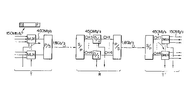
The general construction of the conventional
line terminal equipments T and T' and the conventional
intermediate repeater R are shown in Fig. ~. In the
figure, the transmitting line terminal equipment T
include~ a plurality of multiplexers MU~ each for
multiplexing three 150 Mbfs signals into a 450 Mb/s
signal, and a parallel-serial converter P/S ~or
1 3 ~ 2 ~
convertin~ the f~ur 450 ~b~s pa~allel ~ignals into a
1. ~ Gb/~ ~3rial signal ~ The interm~diate repeate~ R
includ~ a ~erlal-~ar~ l conv~tor SJP for convart~ng
the 1.8Gb/s serial signal into four channels CHl to
CH4 of 450 Mb~s parallel 9ignE1l3, a plur~lity o~ D~I
units ~Gr droppin~ or in~ertln~ n~c~ary ~ub6i~nals,
and a ~arallel-~rial ~onv~rt~r P~S for convertin~ th~
four channels ~f 45~ ~b~s ~Rra~ lgnal~ into a 1.8
ab~s 4¢rial signal I The 11I1Q terminal equi~ment T'
include9 a serial-parallel ~ont~erter S~P for conYertln~
~he 1.~ GbJs serial ~i~nal into four ~hann~18 C~1 to CH
4 of 450 MbJs parallel signsls and a plurality of
dem~lltiplexers DMUX for dsmult~ plascln~ ~h~ 4~0 Mb~s
signQl int~ three 150 M~s signale.
In tho transmitting l~ne terminal equlpment T,
subslgnals are al~o mult~plex~d with the 150 M~/9 main
signal~. In the receiving line t~rminal ~qui~ment T',
sub~ignals are demultipl~x~d by the d~rnult~p?exer~ DMUX.
The above-melltion~d num~er of channels and ths
~0 bit rate6 of ~h~ ~ignal~ ~re of course only ~n exa~npl~
The ~eneral con~truction o~ ~ach D~I unit ~n
the intersn~diate repe~ter R i~ ~hown ln Fi~ 3. In the
flgure, the D~I unlt includes a demulti~lexer (DMlJX) 300,
a multiplexer (MIJX~ 301, and a c~ntrol ~rcu~t ~CC) 302.
26 A part of ~he demul~iplexed s~nals ~rom the
demullclpl~x~r (DMUX) 300 ar~ dropped ~nto the c~ntrol
circult (CC) 302, ~hile ~h~ r~malning ~ignals from the
demultiplexer (DM~3X) 340 ar~ pa~sed throu~h and
dire~tly input to the multi}?l~xer (MUX) 301. From the
control circuit ~CC) 3~2, ins~rting slgnals ~re input
to the multiplexer 301.
For example, the input si0nal ~nput to th~
demultiplexer (~MVX~ 300 i~ a l.B Gb~s ~ignal in which
four c~a~nels of signals of 450 M~/~ ar~ mlultiplexed. In
~he 1.8Gb~s signal, ~ubsiç7nal~ are ~uperimposed on the
respectlve channels of 450 MbJ6 ~ignals. In ~uch a
system, subsi~nals pa~ ng throu~h two or moro
1 3 ~ " ~, ~ ;1
- 14 -
specified channels are required to be dropped or inser-
ted at the D/I units corresponding to the specified
channels.
On the other hand, there are through-channel sig-
nals such as communication data which need not be drop-
ped or inserted at any D/I unit. However, as shown in
Fig. 2, conventionally, the D/I units are provided on the
respective channels regardless of whether or not the
signals are the through-channel signals. Therefore, for
0 the through-channel signals, the D/I units connected to
the channels are wasted.
Further, the circuit for selecting the through-
channel signals must be as simple as possible. However,
conventional circuits for selecting these through-channel
signals are formed by a random logic circuit constructed
of 20 to 30 integrated circuits (ICs) so that the circuit
scale becomes large and is opposite to the requirement to
construct by a simple D/I repeater.
Figure 4 is a block diagram showing an intermediate
repeater for explaining the principle of the present
invention. In the Figure, the intermediate repeater
includes an input unit 1, i.e., an optical receiving unit,
two drop/insert units (D/I) 51 and 52, and an output unit
7.
The input unit 1 includes an opto-electric con-
verter (O/E) 2, a serial-parallel converter (S/P) 3 for
converting a 1~8 Gb/s serial signal into four 450 Mb/s
parallel signals, a matrix switch 4 for switching the
input channels in response to channel selecting signals
SELl to SEL4, and a channel selecting circuit 6.
The drop/insert units (D/I) 51 and 52 have a demul-
tiplexer and a multiplexer arranged back to back as shown
in Fig. 3.
The channel selecting circuit 6 receives channel
preselecting signals (al,bl) and (a2,b2) for preselec-
ting channels to be dropped or inserted from or
~`
- 15 -
into the drop/insert units (D/I) 51 and 52. Each of the
channel preselecting signals is formed by a combination
of two bits, i.e., al and bl or a2 and b2. In response
to the channel preselecting signals, the channel selec-
ting circuit 6 outputs, to the matrix switch 4, the
channel selecting signals SELl = (al,bl) and SEL2 =
(a2,b2) for selecting the channels through which signals
to be dropped or inserted are transmitted and, in addi-
tion, channel selecting signals SEL3 = (al,b2) and SEL4
10 = (a2,bl) for selecting the channels through which no
signal is to be dropped or inserted. Hereinafter, the
channels through which signals to be dropped or inserted
are transmitted are referred to as drop/insert channels,
and the channels through which no signal is to be drop-
15 ped or inserted are referred to as through-channels. It
should be noted that each of the through-channel selec-
ting signal SEL3 or SEL4 is formed by an inverted bit of
the first bit of one of the preselecting signals and an
inverted bit of the second bit of another one of the
20 preselecting signals, This is important for selecting
the through-channels by means of a simple circuit.
The output unit 7 includes a parallel-serial con-
verter (P/S) 8 for converting the four 450 Mb/s parallel
signals into a 1.8 Gb/s serial signal, and an electro-
25 optic converter (E/O) 9.
In operation, the signals through the drop/insert
channels CWl and CH2 are input from the input unit 1 to
the drop/insert units 51 and 52 and are dropped there-
~rom~ The signals to be inserted are input from a
30 control circuit (not shown in Fig. 4) into the drop/
insert units 51 and 52 and inserted into the channels
CHl and CH2.
On the other hand, the signals passing through the
through-channels CH3 and CH4 are transmitted directly to
the output unit 7 without passing through the drop/
insert unit 51 or 52.
.
~` ~ 3 ~
- 16 -
The selection of the drop/insert channels CHl and CH2
or the through-channels CH3 and CH4 is carried out by the
channel selection circuit 6. Namely, in response to the
channel preselecting signals (al,bl) and (a2,b2) for
preselecting the drop/insert channels, the channel
selecting signals SELl to SEL4 are output from the chan-
nel selecting circuit 6 to the matrix switch 4 so as to
control the through-channels CH3 and CH4. In other words,
when the channel preselecting signals from the drop/insert
o units 51 and 52 are (al,bl) and (a2,b2), the channel
selecting circuit 6 generates the channel selec-ting
signals SEL3 (a3',b3') = (al,b2) and SEL4(a4',b4')
(a2,bl) for selecting the through-channels.
Figure 5 is a block diagram showing an optical
transmission system including the D/I repeater according
to an embodiment of the present invention. In the Figure,
a transmitting line terminal equipment T and a D/I
repeater R are connected through an optical fiber F.
Also, the D/I repeater R and a receiving side line ter-
minal equipment T' are connected through another optical
fiber F.
The transmitting line terminal equipment T includes
a plurality of multiplexers 10 each for multiplexing three
lines of 45 Mb/s to a 150 Mb/s, four multiplexers 11 each
for multiplexing three lines of 150 Mb/s to a 450 Mb/s,
a parallel to serial converter (P/S) 12 for converting the
four parallel 450 Mb/s signals into a 1.8 Gb/s signal, and
an electro-optic converter (O/E) 13 for converting the 1.8
Gb/s signal into an optical signal.
The construction of the D/I repeater R is substan-
tially the same as that shown in Fig. 4. In Fig. 5, the
D/I repeater R includes a central control unit (CC) 53
which is connected to a personal computer (PC) 54 to which
a data terminal 55, a telephone terminal 56, a printer 57
and the like are connected. The drop/insert
... . .
~L 3 ~
units 51 and 52 each has a multiplexer and a demulti-
plexer arranged back to back as shown in Fig. 3. From
the D/I units 51 and 52, channel preselecting signals
(al,bl) and (a2,b2) fox preselecting the drop/insert
channels are output to the channel selecting circuit 6.
The receiving line terminal equipment T' includes an
opto-electric converter (O/E) 14 for converting the 1.8
Gb/s optical signal from the intsrmediate repeater R into
a 1.~ Gb/s electric signal, a serial-parallel con- verter
15, a matrix switch 16, demultiplexers 171 and 172
including four demultiplexers 1711, 1712, 1721 and 1722
each for demultiplexing a 450 Mb/s signal into three 150
Mb/s, a channel selecting circuit 18, and a plurality of
demultiplexers 19 each for demultiplexing the 150 Mb/s
signal into 45 Mb/s signals.
Fig. 6 is a block diagram showing the construction
of the D/I units 51 and 52 in the intermediate repeater
R shown in Fig. 5. In the Figure, the D/I units 51 and
52 respectively include frame synchronization detecting
parts 51a and 52a, channel number comparing parts 51b and
52b for comparing channel numbers previously set from
setting terminals 51c and 52c with channel numbers in the
received channels from the matrix switch 4, OR gates 51d
and 52d for gating the outputs of the frame
synchronization detecting parts 51a and 52a and the
comparing parts 51b and 52b, oscillators 51e and 52e, NAND
gates 51f and 52f, and one-fourth frequency dividing
circuits 51g and 52g.
The frame synchronization detecting part 51a pre-
viously outputs an Out Of Frame signal OOF when it can-
not find a frame synchronizing signal FR in the channel
received from the matrix switch 4. The channel number
comparing part 51b outputs a discord signal NC when the
channel number in the received channel does not coincide
with the previously stored channel number. When at least
one of the Out Of Frame signal OOF and the
s ~
- 18 -
non-coincide signal NC is output, it is gated through the
0~ gate 51d to be output as an alarm signal ALM. While
the alarm signal ALM is being generated, the out- put of
the clock oscillator 51e is gated through the NAND gate
51f. The clock-signal oscillator 52e outputs a clock
signal of about several KHz to the NAND gate 51f. The
frequency of the oscillator 51e is determined by the
maximum time required to detect a frame. The maximum time
for detecting the frame is referred to as a Maximum
Average Reframing Time MART, and in this example, it is
about 70~ seconds.
The output of the NAND gate 51f is input to the one-
fourth frequency dividing circuit 51g. The fre- quency
dividing circuit 51g includes two dividing stages. From
the two dividing stages, a 2-bit channel preselecting
signal (al,bl) is output for selecting a channel to be
dropped or to be inserted.
The circuit construction of the D/I unit 52 is the
same as the D/I unit 51 described above. The parts
corresponding to the parts 51a to 51g are denoted by 52a
to 52g. From the two stages in the frequency divider 52g,
a 2-bit channel preselecting signal (a2,b2) is output for
selecting a channel to be dropped or to be inserted.
The channel selecting circuit 6 receives, from the
2s D/I units 51 and 52, the channel preselecting signals
(al,bl) and (a2,b2) for preselecting the channels to be
dropped and to be inserted, and generates the same channel
selecting signals SELl(al',bl') = (al,bl) and SEL2
(a2',b2') = (a2,b2) for selecting the input channels to
be dropped and to be inserted, and also generates the
other channel selecting signals (SEL3(a3',b3') = ~al,b2)
and SEL4(a4',b4') = (a2,bl) for selecting the channels
not to be dropped and to be inserted. These selecting
signals SELl to SEL4 are applied to the matrix switch 4.
Figure 7 is a diagram showing an example of an
lg ~
operation of the D~I unit 51 ~hown in Fig. 6. In Fig. 7,
thc matrix 9~itch 4 has our iPp~t ter~i~als #1 to #4
~nd four output termin~l~ #1' to #4'. It i~ ~sswmed that
the first output termin~l #l' i~ at first connected to
S th~ f~rst i~put ~exm~nal ~1~ to whieh th~ input channel
of the ~hannel numb~r #1 1~ conne~ted ~n re~onse to the
channel ~electin~ ~ignal (al',hl') = ~0,0). It i~ al~o
a~sumed that the channel n~mb~r ~ is previously stored
in the ch~nnel number comp~rin~ ~rt 51b. Then, ~hen the
0 power of the D/I repeate~ ~ 19 turned ONJ ~ince th~
channel numbe~ #l doos not coincide with ~h~ pre~iously
~tored channel numb~r ~2, an al~rm ~ignal ALM
~ndicating a~ ou~ ~f fra~e 6ynchroniza~ion is output
from the NA~D gate 51~. In r~spo~e ta the alarm ~i~nal
ALM, the one-fourth freg~ncy divider 51g generates a
cahnnol preselecting ~i~nhl ~al,~1). The si~nal ~1 ha~
onc-half the ~req~e~cy o~ the eleck si~nal CL, The
~ign~l al ha~ one-fo~rth the fxequ~ncy of the clock
si~nal CL. The eha~n~l ~electing ~i~nal i~ at f~r~t
tllrn~d from (O,Ol to (1,1). In re~ponse t~ this channel
~electing ~ignal (1,1)~ th~ output o~ ~he matrix sw~tch
4 i9 connected to the ~nput channel o~ the channel
number #4. The ch~nnel number #4 also dces not coincide
~i~h the previous1y stor~d chan~el numbsr ~2. Thereore,
th~ ala~m signa1 ALM does not di~ap~oar. The channel
~electlny si~nal i~ ~hen t~rn~d from (l,1) to (170~ SO
that the output o~ the m~lx switch 4 i5 conn~ct~d t~
the input channel o the ~hannQl numbe~ ~3. ~he channel
number #3 also does ~ot ~oin~de with the previo~ly
sto~ed cahnn~l number #~ Therefore, the al~rm s~gnal
al~o does not di appear. ~h~n the chann~l select~ng
s~gnal then be~ome~ (al,bl) - (t1,1) so tlult ~he output
of t~ ~atrlx 4witch 4 1~ connect~d to the input
channel of th~ channel n~b~r ~2, the ehannel numb~r #2
coincides ~ith the pre~iou~ly 6tored channel number #~,
and the~efore, the alanm ~ignal ALM di~appear~. When the
larm ~ignal ALM di~app~ars, t~e 6i~nal o~ the ~hannel
~ 3 1 ~ ~ rJ
o the ohannel number #2 is input to the ~/I unit 51.
Simil~rly to th~ s~3cond, third, and fourt~
OUtpl~t t~rrninals ,~2',#3', and #~', the input chann~ls
~1 to #4 Are ~onnected se~entially in respons~ to the
5 ~hannel Bel ecting slgrla 16 t al ', ~1 ' ), ( a~ ', b2 ' ),
(~3' ,b3~ nd ~a4' ,b4' ) .
~ he operation of another ~JI Imit 52 is quite
slm~lar to that of the D~I unit 51 d~s~ribod above, and
the de~ription ther~of i~ o~itted here.
10Figur~ 8 i~ a diagr~m ~howln~ all combln~t~on~
of the channel selecting signals SELl(al',bl'), 2(a2',
b2'), 3(a3',b3'), and 4(a4',b4'). As will be seen
from Fig. a, when tal',bl'~ - ~0,0), then (a2',b2') may
be (0,0), (0,1), (1,0), or (1,1); ta3' ,b3' ~ may be
15(1,1~, ~1,0), (1,1), or (1J1~; and (~4' ,~ may bs
tl,l), ~1,1), ~0,1), o~ ~0,1), re~pectively. The channe1
ctin~ si~nals (0,0),, (0,1), ~1,0), snd (1,1)
re~p~ctively ~elect the inp-lt channel~ #1, ~2, #3, and
t4 to be connected to the output terml~als of th~
ao matrix switch 4. For the channel selectin~ si~nal
(al',bi3 = (0,1), ~1,0), or (1,1), there are also four
combination~ of eaeh of the ~ther channel sel~tin~
s ignal ~ ( a2 , b2 ), ~ a3 J b3;, nnd ( ~4', b4 ) . ~te that , f or
the ~o~ n~tions of the ~hann~l s~ ting slgnal~
25 m~rked by3~, there ~re 'che ~ame channel sele~ting
slgr~al~ for the dlfferent ~hannels. Thls means that the
sarne input ch~nnel is connected to different output
chann~ls in the matrix sw~ tch 4 . Thls CBUS~8 an
indef~ nite ope~ation of the D~'I unit~ and abnormal
30 operation ~ith re~pec~ ~o the throu~h-ch~nnels. The~
indefinite or abnormal ~per~t~on~, how~v~r, ~ls~ occ~r
e~.ren when the othQr channels ~ele~ting 8y5tem ~8
employed~ Such an ind~finite or ~bnorm~1 operation ~an
be detected ~'c a line terminal egui~men~ and the llk~
~5 by detecting ~n out of rame si~nal OoF. Thexef~e, the
colnbination~ of the ~hannel ~electlng si~n~l~ marked by
~ d~ not c~u3e any problem.
~ 3 ~ ~ ~` J '':k
- 21 -
Figure 9 is a circuit diagram showing an example of
the channel selecting circuit wherein the output chan-
nels C~3 and CH4 are fixed to be through-channels. In
the Figure, the channel selecting circuit 6 includes four
signal lines for directly passing the channel preselecting
signals (al,bl) and (a2,b2) for selecting the input
channels #1 and #2 to be dropped or to be inserted to
output the channel selecting signals SELl (al',bl') and
SEL2(a2',b2'), and four NOT circuits 61 to 6~ for
inverting the codes of the signals on the respective
signal lines. By this construction, the channel selecting
signal SEL3(a3',b3') is determined as (al,b2) and the
channel selecting signal SEL4(a4',b4') is determined as
(a2,bl). Namely, the first bit al in the channel
preselecting signal (al,bl) is inverted by the NOT circuit
61 to output the first bit a3' in the third channel
selecting signal SEL3(a3',b3'); the second bit bl in the
channel preselecting signal (al,bl) is inverted by the
NOT circuit 62 to output the second bit b4' in the fourth
channel selecting signal SEL4(a4',b4'), the first bit a2
in the channel preselecting signal (a2,b2) is inverted by
the NOT circuit 63 to output the first bit a4' in the
fourth channel selecting signal SEL4(a4',b4'): and the
second bit b2 in the channel preselecting signal (a2,b2)
is inverted by the NOT circuit 64 to output the second bit
b3' in the third channel selecting signal SEL3(a3',b3').
Since the channel selecting signals for selecting
the through-channels can be determined by the use ~f only
the channel selecting signals for selecting the drop/
insert channels, the channel selecting circuit 6 can be
formed by a small scale circuit of only two or three ICs.
Figure 10 is a circuit diagram of a channel selec-
ting circuit according to another embodiment of the pre-
sent invention in which a part of the channels are sel-
ectively used as through-channels or drop/insert
- a2- 16~
channels. In the fi~ure, a channel ~eleetin~ circu~k 6a
include~ f~ur ç~te c:ircuit~ 65 to ~B ~ach consistlng of
threc N~ND gate~ and a NOT ~at~ 6~, in ~dditicn to th~
tw~ palr of ~ignal line6 for di~e~tly pa~sing the
chsnn~l cele~ting ~gnal~ ~al,~ ~ and (a2,b2) as the
channel selecting signals SELl(al',bl') and SEL2(a2',
b2") and the four NOT circuits 61 to 64 in the circuit
shown in Fig. 9. A D/I unit detecting signal DT
represents whether or not D/I units corresponding to
the channel~ CH3 and ~4 iæ mounted on the D/I rep~ater
R. When no D~I unit ~orre~pondin~ to th0 channels CH3
and c~4 is rnounted, the det~etin~ si0nal DT is at a hlgh
leYal H, and ~hen the Df I un~ t~ corres~ondlPg to the
ch~nnels cH3 and CH4 i~ mounted, th~ detwt~ng signal
iB at a low le~el L.
Nhen the det~cting signal ~T i-~ at the high
level H, ~he s~ate eircuit 65 ~elects the out~ut ~f the
NOT clrcuit 61, i.~., Rl, as th~ fi~st bit a3' of the
channel sel~ct~ ng ~ignal SEL3; the gate clrcuit 66
ao seleets the output of th~ N~ circuit 64, ~.e~, b~, as
the second bit b3' of l~he ch~nnel sRl~ct~n~ si~nal
SEL3; thq ~tP circuit 67 ~el~ct~ th2 output of the N~
circuit 63 i.e., a2 as the first bit a4' of the channel
selocting signal SEL4~ and the gate circuit ~8 selec~-~
as the output of the N~T circuit 6~ i.e., bl, a-~ the second
bit b4' of the ~hannel e~lec~lng sign~l ~EL4. As a
result, in this ca~e~ the cl~nn~l 6~1ectln~ signals SE;~3
~nd the ~;EL4 ~re the ~me a~ thos~ in the channel
~electin~ çircuit ~ho~m in FIg. 9.
~hen the de~cting signal D~r ia at the low
level L, the gate c~rcu~ts ~5 and 66 sela~t the channe1
select~ng ai~nal ~a3, b3) from the additlon~l D/I
unit~ and the g~te c~rcuit~ ~7 and 6B select tho
channel selecting ~i~nal (a4, ~4~ from the Pdditlonal
3 5 P~I un~ t~ .
The add' tional ~/I un~t~ are u~d in a
repe~t~r which has no through-chann~31. Th~ ~wit~hing
.....
-23-- 13~2~
NOT gate ~9 and the gate circuits ~5 to 68 are provided
for selecting the channe] selecti.ng signaLs SEL3 and
S~L4 to be (al,b2~ and (a2,bl) or (a3,b3) and (a4,b4)
as descri.bed above. Namely, in the repeater which has
no through-channel, there may be further provided two
drop~insert units co.rresponding to the two output
channels ~H3 and CH4 of the mat:rix switch 4 so that all
of the channels are dropped and i.nserted~ Each of tne
additional ~I u.nits has the same constructions as the
D~I uni-t 51 or 52 except for the previously stored
channe] number. A channel selectin.g signal
SEL3(a3',b3~) is the output of one of the additional D~I
unit (not shown in Fig. 10 but may be connected to the
output channel CH3 of the matrix swi-tch 4). A channel
selecting signal SEL4(a4',b4') is the output of another
one of the additional D~-[ unit (not shown in Fig. 10 but
may be connected to the output CH4 of the matrix switch
4). When the additional D~I units are plugged into the
system, the detecting signal DT becomes the low level L.
In contrast, when the additional D~I unit~ are not
plugged into the system, a detecting signal DT becomes
the high level H. Whereby, when the above mentioned
additional D~I units are not plugged into the system,
the gate circuits 65 to 68 select the through-channel
selecting signals SEL3(a3',b3'~ = ~al,b2) and
SEL4(a4',b4') - (a2,hl) which are obtai.ned by inver-ting
the channel selecting signals (al,bl) and ~a2,b2) by
the N~T gates 61 to 64; whereas when -the above mentioned
additional D~I units are plugged into the system, the
gate circuits 65 -to 68 select the channel selecting
signals SET,3(a3',b3') = ~a3,b3) and SEL4~a4',b4') = ~a4,
b4) which are obtained directly from the additional D~I
units or the demulti.plexers.
Fiure 11 is a circuit diagram showing a
general purpose channel selecting circuit according to
still another embodiment of the present invention. In
the above-described embodiments, the through-channels
---24~ 5~
in the intermed;at:.e repeater are fixed to be the
channels C113 and C~4~ The -through-c}lanneLs, however, may
alternat;i.~el.y be any of the chanrlels CHI, CTI2, CH3, and
CH4. The channel. selecting ~ircuit in this case :is as
shown in Fig~ 11.
In Eig. 11, the general purpose channel
selecting circuit 6b includes NOT circuits 61A to 64A
and 61B to 64B for inverting the signal codes of the
channel selecting signals lal,bl), (a2,b2), ~a3,b3),
and ~a4,b4) from the corresponding D~I uni-ts, gate
circuits 65A to 68A and 65B to 68B each consisting of
three NAND gates, and switching NOT gates 69A-1~ 69A-2,
69B-1, and 6~R-2~
There are three modes regarding whether or not
the drop~insert units cvrresponding to the channels ~ll
to CH4 are plug~ed into the sys-tem. Namely, in the
~irst mode, all of -the dropfinsert units are plugged in;
in the second mode, only the drop~insert units
corresponding to the output channels CH1 and CH2 are
plugged in and the drop~i.nsert units corresponding to
the output channels CH3 and CH4 are not plugged in; and
in the third mode, only the drop/insert units
corresponding to the output channels CH3 and CH4 are
plugged in and the drop~inser-t units corresponding to
the channels CH1 and CH2 are not plugged in.
In the first mode, the detecting signals DTA
and DTB are both at the L level and therefore the
outputs of the NOT circuits 6gA-1 and 69B-1 are at the
H level, so that the gate circuits 65A to 68A select the
signals al, bl, a2, and b2 as th~ channel selec-ting
signals SELl(al',bl') and SEL2(a2',b2'3, and the gate
circuits 65B -to 68B select the signals a3,b3,a4 and b4
as the channel selecting signals SEL3(a3',b3') and
SEL4(a4',b4'~. As a result, the channel selecting
signals SEL1 to SF,L4 in this case are (al, bl), (a2,b2~,
(a3~b3), and ~a4, b4) from the D~I units, respectively.
In the second mode, the output of the NOT
2 6 ~ i3 Sd ~
clrcult 6gA-1 and the ou~put cf the Nar circ1t 69B-2 are
a~ the H lovel so that the g~te circuits 65A to 6BA
select th~ ~ignals al, bl, a~, and b2 as the ch~nnel
selectiNg ~ignal~ ~;ELl(al' ,~1' ) and SEL~(a2' ,b2' ), and
5 the gatc circuit~ ~5B to 68E~ 8~1B~t the ~ignal~
al,b?,a2, ~nd bl a~ the ~i~na1~ ~L3ta3' ,b3' ) and
SEL~a4' ,b4' ), respectiv~ly, A~ a r~sult, the channel
sele~:ting slgn~ Ll to SEL4 In this cas~ are (al,
bl), (a~,b2), ~a1,b~), and (a~, bl~, r~pectlYely.
The a~o~e- ment1oned f~r61; and ~econd mode~
are the sa~ne as the pr~-~iously d~cribed er~odiment.
In th~ third mod~, tha output of th~ ~OT
~lrcult 69A-2 and the ollt~ut of the ~OT cir~it 69B-l
ar~ at the H le~el ~o th~t th~ gat~ circllit~ 65A to 68A
15 ~elect the signals a3, b4, ~4, and b3 as the channel
sel~cting signals SELl(al' ,bl' ) and SE~2(aZ~ ,b2' 1, and
the gate circuits ~5s to 68B ~lect the ~i~nals a3,
b3,a~, Qnd b4 as the cha~n~l s~lectln~ si~nal~
SEL3(a~ ,b3' ) and S~L4~a~ ,b4' ~, respectiYely. As ~
2~ result, ths channel selectlng sign~ls SELl to SEL4 in
this ca~e ar~ (a~, b4), ( a4, b~)~ (a3, b3), and (a4,
b~ ), respe~ti~ely ~
The abo~e-describsd embodim~nt~ of th~ chann~l
~eleetlng circuits ~ho~n in Fi~s. 1~ and ll can bc
25 applied not only to the i~te~m~diat~ ~e~ater but E~190
to the recei~n~ lina terminal ~uipment T'. Therefore,
both the re~ei~rin~ lin~ t~rminal equipment and the
interm~diate repe~ter ~an employ tho ~am~ channel
selecting c~rcuit. ~ote, howev~r, that, in the re~eiv~ng
30 line te~minal e~uip~nent T', demultipl~xe~ are u~ed in
place of the D/I un~t~ in the intsrm~diat~ r~p~atcr ~.
The D~I ~lllitS and the d~multiplexer~ are csmmon in
their multi~lexing function. Since the channel selecting
c1rcult in the recelving line t~rminal egu~ment and in
35 the intermediate repeater can b~ manufactured as the
same cir~uit configuration wlth the ~ame design
specification, t~ cost for implementing an ~tical
` - 26 - ' 1 3 1 ~5 2 4
~: `
transmission system can be reduced in, for example, the
design cost or in the manufacturing cost of the
`~` repeaters. Further, when the channel selecting circuits
are made the same, the number of kinds of standby units
of the repeaters can be reduced so that the management
becomes easy.
In the above-described embodiment with
reference to Fig. 11, the through-channel may be any
one of the output channels CH1 to CH4. As a result, the
insert/drop operation between the line terminal
equipment~iand the intermediate repeater can be effected
flexibly,~providing a great advantage in decreasing the
design cost, the manufacturing cost, managing cost, and
the like. ~
In the above described embodiments, after the
drop~insert channels and the through-channels are
determined, if one or more of the channels received by
the intermediate repeater or by the recelving line
; ter~minal~;equipment enters a state of out of frame
20~ ~synchron1zation, or~in other words an out of frame, due
to a fault in the transmitti~ng repeater or the
transmittig line, external noises and the like so that
the~intermediate repeater R or the~receiving repeater T'
receives~ an incorrect channel, the intermediate
repeater~R~or the receiving line~terminal equipment T'
serches ~the~ desired channel from all of the input
channels.~ To this end, the intermediate repeater R or
the receiving line`terminal equipment T' carries out a
switching operation for all the channels. By the
; 30 switching~~operation, however~,~the correctly selected
channels such as through-cahnnels are also switched. As
a result, even when a single input channel includes a
A~ ~` fault, all of the channels in the whole system become
disconnected. Therefore, the above~described
embodiments still have a low system reliability. -
In the following, a still further embodimento the present invention is described. An object of
~: ~ :Z '~:
~ ,.
~: `
- , `
:
- 27 - ~ 3~ 2
thl~ embodiment of the ~re~ent in~Qntion i~ to pr~en~
the disc~nnected ~tRte~ o~ the all channel~ ~ven when a
sinyle channel has a fault and to rai~e the sy~tem
rel~a~llity. To attain th~s ~b~ct~ accord~n~ to this
S embodiment, bri~fly, when Q channel is not correctly
~ecei~d by an intermediate repeat~ or ~ receiYlng ltne
terminal eguipment, the channel ~ s~itched to another
~hannel in the matrix swit~h, whlle the thr~ugh-channel~
are f~x~d so a5 not to b~ ~witched~
Fig~re 12 is a bloGk diagram showin~ ~ DfI
unit in an ~ntermediate ~epeatex according to this
embodiment of the pregen~ lnvention. In the f~gure, the
~ame parts as in the ~/I untt 51 ~hown in Fi~. 6 are
denoted by th¢ ~ame ref~renc~ ~ymbol~, and the parts
15 coxresponding to the p~rtg ~hown in Flg. 6 are denoted
~y the s~me referen(:e ~umber~ with primes.
Namely, gl' 19 a ~fI un~t a~cording to this
~mbodiment. S10 is a demult~plex~r for d~ul~iplexin~
the ~ignal~ pas~ing through the ~hannsl cHl output from
~0 th~ matr~x switch 4 into ~ plurality of main ~l~nals.
~he dem~ltiplexer 510 al~o dete~ts an out o~ frame
~nchroni2ation signal OOF and a ~-blt channe~ numb2r
in the ch~nnel CH1. Sll i6 an out of fram~ protecting
circuit for ef~e~ting a fron~ and raar protection of
the out o~ fr~me ~ynchroniza~ion ~i~nal OOF detected by
the dem~ltiplexer 510, 51~ i~ a co~parin~ oircult for
de~ecti~g ~Thether or not the received cha~nel number
from the de~ultiplexer 510 ~olncld~s with thn
prevlou~ly ~tored 2~bit channel ~elQction number, and
51~ i~ a non-coincidence gignal protection circuit for
~e~in0 a frcnt and r~ar protection of th~ 5ignal ~
represent~n~ that the r~eived channcl nwmber does not
co~n~id~ with the previou~ly 9Rt channel selection
number, det~ct~d by the ~omparin~ circuit 512. 51d ~
3S an OR circuit for obtaining Q lo~ical ~m o~ the outp~t
siynal o~ the out of fram~ protectlon cir~uit 511 and
the output signal of the non-coincidence signal protecting
,~
~ 3 1 ~ ~r3 ~ ,
--28 ~
circit 513 to be output as an ~ut of frame
synchroniæation signa~ ~OF, and 515 i~ a reframe
protoction circllit fo~ ~3ffect1 n~ a rea~ protectlon of
th~ output ~ignal f rorn the OR circuit Sld and ~or
S outputting the out of ~rame ~yn~hronization ~igxlal OOF
to the matrlx switch 4-
51e i9 ~ clock~ignal osc~llator. 5ig is a~requency divider which ~ reset by the out o~ frame
synchronization signal o~F from the OR circult 51d. S18
10 1~ a ~unter f or countin~ ~he %lax~ m ~rerage
r~fr~mining time MART ~ultiplied by two ~fter the reset
and ~enerate6 a 2-bit eh~ l selecting ~ignal. Th0 2-
bit channel selectin~ signal appl~ed to th~ counter 51B
~ tput ~ro~ the c~unter 51~ after c~untin~ th~ MART
15 and 15 applied to a channel ~electing circult 6'.
T~e demultiplexer 510 ~n Fi~. 12 ~ncludes the
frame synchronizat~on de~ectlng cireult 51~ in tho D/I
unlt 51 shown in Fig. ~ T~e con~titut~on ~nd the
functi~n of the compar~ng circuit 512 i~ the oame as
tho~e of the co~paring eircuit 51b shown ~n Fig. 6.
The oth~r D~I units 52', S3' ~nd 54' have
similar constitutlon a~ the ~I unlt 51'.
~ hen the ~I un~t i5 tn~erted into the system,
a dete~ting signal DTA of the L level i~ in~ut to the
as channel sel~ting circuit 6 ' ~
F,igllre 13 i~ a blo~k diagram showlng the
detailed cons~ruction of the a\atrix ~witch 4' ~nd the
channel Belecting circut t 6 ' in the lntcrmed~ ate
repea~er ~. In the figure, 471 to 4~4 are s~Yitching
30 parts constituting th~ matrix s-Yitch 4 ' . ~he
constru~tion of the chann~l s~lecting circuit 6 ' i~
8ubstantially the ~ame as that ~ho~n in Fig. 11. ~amnly,
475 to 47B E~r~ channel ~el~ctor~ in ~he chann~l
~electlng ~:ircuit 6 ' . The ~hannel ~lector 475 i~
35 formed by the logic eircuit~ 65A arld ~6A shown ih Fig.
11. Simt l~I ly, the channel s~lector4 476 to 47~ are
forrned by the logic circuits 67A ~n~ SBA, 65B ænd 66B,
--29 ~
and 67B and 68B, respectively. To ~he channel ~elect~rs
47S to 47B, the l~ve~ting ~ircult~ 61B to ~4B and 61A
to 64A are connect~d in the ~ame way as ~n F~g~ 11. The
out of fralne synchronizat~on ~31gnal OOF from the
re~ram~ protectian unit 515 ln the l)~I unit 51 ' 15
applled to the s~tchin~ p~rts 473 a~d 4~4 corresponding
to the throl~gh-chann01s, Similarly, the signal OOF ~rom
the D/I unit 5~ also ~p~lied to the swltching parts
473 ~n~ 474 corre~pondin~ to the through-ch~rlnela. Dr
10 is a detectiorl s~ynal repre~enting whethe~ ~r not the
eorresponding ~/I unit ls mourlted in the system. MAIN
5IG is a main signal in the select~d channel from the
mat~ix swltch 4'. ~ch af ~he ~Yit~hlng part:~ 4tl.to
4?4 sel~cts one of th~ four inpllt c~annele input ~rom
15 the serial-~ar~llel con~erter 3 and outpllt ~t ~n
~c~ordance with the oorrespondin~ one of the ~electing
signals from the selecting parts 475 and 478. In addi-
tion, according to this embodiment of the present inven-
tion, when an out of frame synchronization signal OOF
ao from the D/I unit 51' or 52' is received, the switching
parts 473 and 474 corresponding to the through-channel
fix their switching positions so as to continuously
select the channels which are being selected, regardless
of the channel selecting signals from the selecting
2~ parts 477 and 478.
In th~ rna~rix s~ikch 4', th~ sel~ct~on of the
channel num~ers of the through-ch~nnsl at ~ normal 6tato
i8 earr~ ed out in th~ ~me way as ~n ~he ~efore.
described embodiment ~ith reference to ~Lg. 11- ~amely,
30 in thls ca~e, no out o~ frqme signal OOF i~ gen~rated
so that the s~itchlng parts 471 to 47 4 operate to
select the ch~nnels in accordance wl~h th~ ~hannel
sE~lecting signalx in the ~ 3 w~y a~ de~cribed befor~.
By contrsst, wh~n an out o~ ~ram~
~5 synchronization ~iynal 00~ eneraked from either one
of the ~ nits 51' and 5~' due to eome hard ~rror o~
~oft error, the channel selection in the ~ ehing
.
30-- ` 13~5~
parts 473 and 47A corresponding to t;he throug~-hannels
are inhibited to sequential.ly select -the channels but
-their output channels are fixed to the channels bei.ng
selected at the time the signal OOF is applied, while
the other switching parts 471 and 472 which do not
correspond to the through-channels continue to select
-the input channels until the signal OOF disappears.
Assuming that a fault occurs in the
multiplexer 11 ( see Fig. 5~ in the the optical line
terminal equipment T so that the channel CH1 enters a
fault state, arld that the D~I unit 51' in the optical
intermediate repeater R expects the channel CH1 as a
drop or insert channel, as a result, the D/I uni.t 51'
cannot receive the channel CH1 in a normally
synchronized state. Namely, the ~I unit 51' cannot
detect the frame signal in -the channel CH1 or cannot
detect the chan.nel number of the channel CH1. In this
situation, the ~I unit 51' outputs -the out of frame
synchronization signal OOF after a predetermined
protection time formed by the OOF pro-tection circuit 511
The signal OOF is applied to the switching parts 473 and
474 whereby the operations thereof are inhibited. Then
the D~I unit 51' outputs a cha~mel preselecting signal
(al,bl) to the channel selecting circuit 6' so as to
receive other channels fo.r searching the desired channel
CH1. In response to the channel preselccting signal,
the matrix switch 4' switches the output channels.
An operation of the device shown in Figs. 12
and l3 is described in more detail with reference to
Figs~ 14 and 15.
Figure 1~ is a diagram for explaining the
output timing of the channel selecting signal and the
out of frame synchronization signal OOF. In the figure,
before a time tl, the channel CHl is in a normal state
so that the OOF signal at the output of the
demultiplexer 510 is at the low level L. When a fault
occurs in the channel CHl at a time tl, an OOF signal
~3~ ~21;~
- 31 -
is applied from the demultiplexer 510 to the OOF pro-
tection circuit 511. The OOF protection circuit 511 is
provided because there is a possibility that the OFF
signal will disappear within a short time. If the OFF
signal disappears within a short time and the normal state
returns soon, the channel selection is not necessary.
Therefore, to avoid the unnecessary selection of the
channels, the OOF signal is output from the OOF pro-
tection circuit 511 at a time t2 after a predetermined
front protection time pl from the time tl. Here, the
front protection means the ensurance time of the begin-
ning of the OOF signal. At the same time tl, the com-
paring circuit 512 also detects that the channel number
in the received channel does not coincide with the pre-
viously stored channel number. The non-coincidence signal
protection circuit 513 also performs the front protection
of the non-coincidence signal. As a result, at a time t3
after a predetermined protection time p2, the non-
coincidence signal protection circuit 513 outputs a high
level signal indicating that the channel number in the
received channel is uncertain. The period pl is selected
to be shorter than the period p2 because the front
protection of the non-coincidence usually requires a
longer time. As a result, the OR circuit 51d outputs, at
the time t2, the OOF signal which is then applied as a
reset signal to the frequency divider 51e. The frequency
divider 51g then counts to two times the MART by the use
of the clock signal generator 51e. The output of the OR
circuit 51d is also sent through the reframe protection
circuit 515 to the matrix switch 4.
The channel selecting signal is changed after the
two times of the MART after the time t2. Here, the worst
average reframing time MART is the average time from the
time when the received signal detects the out of frame
synchronization state due to a bit error or external
noises on a transmission line and the like during a normal
state, to the time when a synchronized
,:
i.
--32- 13~ ~ ~2l~
state is again recovered.
Namely, the out o~ frame synchronization
signal COF from the o~ circuit 51d drives the frequency
divider 51g so that the frequency of -the clock signal
from the clock-signal oscillator 51e is di~ided. The
divided frequency signal is sent to the counter 518. The
co~mter 518 outputs a channel selecting signal ~al,bl)
to the channel selecting citcuit 6' after counting the
worst average reframe time by the use of the input
clock signals.
In the matrix switch 4', the out of frame
synchronization signal OOF is input to the switching
parts 473 and 474, whereby the frames being selected by
these switching parts ~73 and 474 are fixed not to be
switched. To the selecting parts 475 and ~76, the
channel selecting signals ~al,bl~ and (a2,b2) are input
at a time t~ after the the M~RT has passed twice from
the time t2 when the signal OOF is applied from the OR
circuit 51d to the frequency divider 51g so as to change
the channel selecting signals at the output of the
selecting parts 475 and 476, whereby, the switching
parts 471 and 472 select the other channels and send
them to the ~I units 51' and 52'. The switching parts
~73 and 474 fix their OUtplltS as the through-channels so
that the channel selecting is not carried out.
Next, an explanation of the operation of the
optical intermediate repeater ~ is given for the case
when the channel CH1 is reframed or recovered from its
fault state.
Figure 15 is a time chart for explaining the
reframe process from the out of frame state~
In Fig. 15, when the channel CH1 becomes
normal at a time tl, the demultiplexer 510 detects the
frame synchronization signal ~R in the received channel
CH1 so as to output a frame detection signal which is
the L level of the out of frame synchronization signal
OOF to the out of frame protection circuit 511 which
~ 3 ~ ~ ~ 2 ~
- 33 -
then turns the signal OOF at its output at a time t2 after
a predetermined rear protection time p3 has passed. Here,
the rear protection time p3 means the ensuring time of the
fall of the signal OOF. Similarly, at the time tl, the
comparing circuit 512 detects a coincidence of the channel
number of the channel CHl with the previously stored
channel number so as to drive the non-coincidence signal
protection circuit 513 which then stops, at a time t3, to
provide its output signal afte~ a predetermined rear
protection time p4 has passed. Therefore, the out of
frame synchronization signal OOF output ~rom the OR
circuit 51d, is turned off only after both of the output
signals from the frame synchronization protection circuit
51 and the non-coincidence signal protection circuit 513
are turned off. In the case of Fig. 15, it is the time
t3. Further, the reframe protection circuit 515 turns
off the out of frame synchronization signal OOF output to
the matrix switch 4' only after a predetermined reframe
protection time pS has further passed.
The above-mentioned reframe protection time p5 is
provided because the non-coincidence signal cannot
correctly be obtained until the frame synchronization is
stably established. Therefore, as shown in the lower
portion in Fig. 15, the channel identification coinci-
dence signal may be indefinite even after the frame
synchronization protection time p3 has passed. This
indefinite coincidence/non-coincîdence signal may cause
a disturbance of the operation of the matrix switch 4'.
To avoid the disturbance, the reframe protection time p5
is further provided as shown in Fig. 15.
Various modifications are possible in implementing
the present invention. For example, the present inven-
tion is not restricted to the optical communication sys-
tem as in the above-described embodiments but may be
applied to other communication
---3~ 3~
systems. F~lrther, the present inventioll may be appli.l.~d
not o:nly -t-o an i.ntermediate repeater but also to a
receivi.ng line terminal equipment~ When the present
i.nvention is applied to a receiving line terminal
equipment, demultip]exing units should be used in place
of the D~I units in the i.ntermediate repeater. ~till
further, the present inven-tion may employ, as the
multiplexing system, a f:requency divided multiplexing
system, a wavc length dividing multiplexing system, and
the like.
As described in detail above, in the
drop~insert cahnnel selecting system accorcing to the
present invention, the channe] selecting signal is
expressed by a 2-bit signal ~a,b). When subsignals on
two specific channels are to be dropped or to be
inserted in an in-termediate repeater, the channel
selecting signals for selecting the channels to be
dropped or to be inserted are assumed to be ~al,bl~ and
(a2,b2), then the channel selecting signals for
selecting the channels which are not to be dropped or
inserted are calculated as (a2,bl) and (al,b2).
Accordingly, the conventional random logic circuit
constructed by 20 to 30 ICs is not necessary, and
through-channels can be selected by a small scale
circuit with only 2 to 3 ICs. Further, according to the
present invention, in a multi.plexing transmission
device, even when one line becomes faulty, all lines do
not become faulty. Namely, as descri.bed above, since
the channel selecting signals are switched after a
sufficient protection time from the detection of the
out of frame signal, and si.nce the selecting parts
corresponding to the through-chanels are fixed so as
not to change -the channels, the main signals passing
through the through -chann.els are not cut even when a
signal OOF is detected in the other channels~