Note : Les descriptions sont présentées dans la langue officielle dans laquelle elles ont été soumises.
1311821
ASYMMETRIC MODE FILTER
Fiber and integrated optic devices are being rapidly developed
into csmponents for use in waveguide circuits. Such optical waveguide
circuits are usually characterised by a dielectric medium which carries
5 electromagnetic radiation, usually in the optical spectrum along
predetermined paths or conduits. These dielectric waveguide conduits
are surrounded by a second dielectric medium with dielectric properties
adjusted to cause electromagnetic radiation propagating through the
waveguides to remain within such waveguides. For fiber optic devices
10 this second medium takes the form of the cladding immediately
surrounding the conducting fiber. For integrated optics devices, the
substrate material and the air over the substrate usually serve as the
second madium.
BRIEF DESCRIPTION OF THE DRAWINGS
Figure 1 shows an optical circuit for a Sagnac interferometer using
a single Y-integrated optic coupler as practiced in the prior art;
Figure 2 shows an optical circuit for a Sagnac interferometer
utilizing an integrated optic chip containing a double Y configuration
which has been proposed in the prior art for use in such interferometer
20 circuits;
Figure 3 shows an integrated optic chip constructed with a double
Y waveguide on its surface and depicting the origination of stray
radiation from a Y-junction;
Figure 4 shows an optical circuit for a Sagnac interferometer
25 which contains an integrated optic chip with a double Y configuration and
displaying the energy balance between the conducted radiation within
the waveguide and the leaked radiation;
Figure 4A shows a cross-section through the integrated optic chip
containing an embedded layer of material for intercepting the radiated
30 energy from the guiding waveguide on the surface of the chip;
Figure 4B shows an alternative cross-sectional view with a phase
matching medium and an absorbing medium embedded in the substrate;
~'
.~
1311821
Figure 5 shows a double Y waveguide circuit on a substrate with
polarizing and modulating electrodes configured on the surface of the
substrate;
Figure 5B shows a cross section view at B-B of modulating
5 electrodes placed within the substrate to intercept the antisymmetric
radiation; and
Figure 6 shows a double Y waveguide circuit with modulating
electrodes placed at each Y-node.
In the field of interferometry, heavy use of fiber optics and
10 integrated optic devices is becoming common. An example is the
Sagnac interferometer wherein rotation rates about a given axis are
accurateiy measured. A Sagnac interferometer is shown in Figure 1
where source 60 directs light through fiber coupler 64 and waveguide 66
onto integrated optic chip 68, which contains Yjunction 72. The Y-
15 junction splits the light beam into two beams which will traverse loop 70in counter-propagating directions. It is the rotation about an axis
perpendicular to the plane of loop 70 that is to be measured.
A rotation of the loop causes a change in phase between the
counter-propagating beams. When the beams recombine at Y-junction
20 72, they are propagated back along waveguide 66 and are coupled
down to detector 62. Detector 62 sensqs the intensity change resulting
from the phase shift occurring in the combined beams and registers such
as a measure of the rotation or rotation rate of the interferometer.
Recent work on such interferometers has utilized fiber optic
25 components throughout, i.e. the integrated optic device 68 containing
Y-junction 72 would be a second fiber optic coupler 64 as depicted in
Figure 1. Such coupler would split the incoming beam of light and then
recombine it after propagation through loop 70.
The desire to replace fiber optic devices with integrated optic
30 devices has been fueled by the anticipation of better miniaturization
capability and lower costs in producing such devices.
1311~21
A preferable configuration for a Sagnac interferometer is shown in
Figure 2. In this figure fiber optic coupler 64 and waveguide segment 66
have been replaced by integrated optics component 30. Integrated
optics component 30 is configured with two Y-junctions 40 and 42, and
connecting waveguide segment 41. Source 34 and detector 36 are
directly attached to integrated optics ship 30 at the respective legs of the
first Yjunction 40. The second Y-junction 42 functions as the prior Y-
junction 72 in Figure 3 by splitting the input electromagnetic beam into
counter-propagating beams in fiber loop 32. The returning counter-
propagating beams are recombined by junction 42. The combined
beams are then returned along waveguide 41 to detector 36 through the
first Yjunction 40.
Many active or passive functioning components may be built into
integrated optic chip devices such as 30. For example, polarizer 38 is
1 5 shown built-in across waveguide segment 41, and modulating device 48
is shown built-in on the outbound leg 46 of the second Y-junction 42.
Such elements are necessary to adjust polarization and modulation
- factors on the electromagnetic or light beams propagating the optical
waveguides.
The obvious beneficial factors of using an optical chip 30 with two
Y dividers has been impossible to achieve because of a known problem
with radiation leakage into the substrate from the Y-junctions. Figure 3
shows an integratad optic chip 10 with a double Y-junction waveguide
constructed upon it. Considering conduits 16 and 18 as input waveguide
legs to Y-junction node 12, we see that light coming in along one or the
other of thsse conduits is joined and forced to continue along a single
connecting waveguide conduit 28 to a second Y-junction node 14. At
noda 14 the beam is split into separate beams to propagate out legs 22
and 20.
- 30 The problem occurs primarily at Y-junction node 12 where light is
radiated from the junction into the substrate. This radiated energy is
generally directed away from the waveguides at a small angle and would
normally continue into the substrate material of integrated optic chip 10.
~'
. .
1311~21
Hows\/er, a small but significant portion of this radiated energy 24
is coupled back into those waveguide portions downstream from Y-
junction node 12. Prior research has shown that this energy 26 re-enters
the waveguide configurations along waveguide element 28, at Y-junction
node 1, and in both of the waveguide conduits 20 and 22.
A technical analysis shows that light entering either of the single
mode waveguide conduits 16 or 18 is composed of a symmetric mode
and an antisymmetric mode of energy. At Y-junction node 12, the
symmetric node is allowed to continue propagation within waveguide
conduit 28, but the antisymmetric mode is stripped away and caused to
radiate into substrate 10. In Figure 3, then, stray radiation 24 represents
this antisymmetric mode energy.
This phenomenon has been well presented in prior U.S. patent
4,468,085 by Papuchon, et al. and in the article ~Reciprocity Proper~ies of
a Branching Waveguiden by H. J. Arditty, M. Papuchon, and C. Puech, pp.
102-110, Fiber-Optic Rotation Sensors and Related Technologies, edited
by S. Ezekial and H. J. Arditty, Springer-Verlag, 1982.
The phenomenon results in bias errors of hundreds of
degrees/hour in Sagnac interferometers and therefore makes such an
integrated optic double Y-structure architecture unsuitable for use. This
error source strongly limits accuracies that may be achieved in
interferometric applications. The present invention provides apparatus
and methods that eliminate or greatly reduce this error.
SI~MMARY OF THE INVENTION
The present invention discloses methods and devices which
cause the radiation energy (antisymmetric mode energy) to be
intercepted and absorbed or directed away from possible recoupling
back into the circuit, or which cause differential modulation between the
radiated energy and the guided energy (symmetric mode energy) to be
effected. The invention presents construction of integrated optics ShipS
containing Y-junctions with one or mors layers of absorbing media
placed in the substrate material and configured to intercept and absorb
1311821
the radiated stray energy, thereby eliminating its possibility of recoupling
into the waveguide at a later point.
A second approach allows the stray radiation to be recoupled
either accidentally or deliberately back into the optical circuit of the
5 interferometer of Sagnac device. However, the stray radiation is shifted
by differential modulation between the stray and guidsd waves to a
region outside of the bandwidth of measurement in the optical circuit of
interest. The invention also provides the capability of differentially
modulating a unique characteristic of the stray radiation, e.g.,
10 polarization, such that an error component caused by the stray radiation
could be demodulated and removed in the detection circuit through
signal possessing schemes applied at that point.
~EFERRED EMBODIMENT OF THE INVENTION
The invention embodies a device and method wherein the
15 radiation electromagnetic energy (the antisymmetric mode energy) is
intercepted and absorbed, or is altered in a way to eliminate it as an error
source in the optical path of the interferometer circuit. Absorbing the
spurious radiation has the effect of eliminating the possibility that it may
couple itself back into the optical circuits waveguides. Modulating or
20 otherwise altering the nature of the light that has spuriously radiated from
a Y-junction allows the opportunity to process out any error if such
radiation should re-enter the interferometric optical pathway.
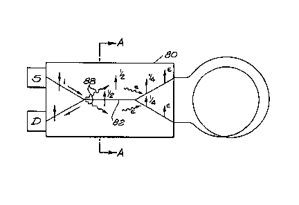
Referring to Figure 4, the double Y configuration is shown installed
on an integrated optics chip substrate 80 in a circuit comprising a
25 Sagnac gyroscope. The energy coming from the source will have a
nominal intensity I as indicated in the figure. One half that energy will be
radiated out from the first Y-junction as also indicated. Some of that
energy radiated from the Y-junction will find its way back into the Sagnac
optical circuit downstream from the Y-junction as an error source
30 epsilon, E.
As seen in the diagram, one half of the nominal source energy is
equally split by the second Y-junction into each of its outbound legs, and
drops to one-quarter of the intensity emined from the source. This portion
1311~21
also includes the spurious error source E. As a result two beams with
approximate intensities equal to one-quarter of the original source
intensity plus some coupled error component now propagate in
opposite directions around the Sagnac loop 70.
These guided beams are recombined by the second coupler, and
then the combined beam is conveyed to the detector. The combined
beam returning along waveguide 82 now contains energy components
which have been completely subjected to the waveguide architecture of
the circuit and have been treated to guarantee that reciprocity is
preserved. Error components which have partially been transmitted
outside the circuit are not subject to reciprocity control. It is this error
component which causes unacceptable errors at the detector.
A cross-section of substrate 80 is shown in Figure 4A. At the point
of the cross-section taken Just after the first Y-junction, waveguide 82 is
shown embedded in surface of the substrate 80. The intensity carried by
the waveguide is indicated by the arrow with the fraction 1/2 adjacent to
it. The radiation energy is depicted by the wavy lines directing away from
the waveguide 82 and, as depicted, one half of the intensity is also
carried into the substrate.
The radiated energy 88 has been found to be directed in a rather
confined solid angle whose direction is sloped downward from existing
waveguide 82 as the radiated energy propagates through substrate 80.
Placing within the substrate an absorbing layer 84 at a depth d
indicated by the reference numeral 86 provides for intercepting and
absorbing radiation 88. With the absorption of the radiation, very little if
any amount is scattered back into the gyro optical circuit to cause error
problems. This absorbing layer 84 can be an absorbing structure of
multiple independent layers, or can also be formed as a two or three
dimensional absorbing structure.
If layer 84iS specifically designed to absorb the spurious radiation,
its shape and location need only to be controlled by the necessity of
being located outside the evanescent field surrounding waveguide 82
and within a distance to intercept the radiation energy 88 effectively e.g.,
1311~21
at a distance of one millimetsr from the Y-junction the radiation may be
expected to have reached a depth of 17 microns into the substrate.
Therefore, at this point the absorbing medium should be placed between
2 and 17 microns from the conducting waveguide on the surface of
5 integrated optics substrate 80. Methods of placing such a layer into a
substrate used in optical waveguides such as LinbO3 or InGaAs are
many and well known in the art. Physical methods of mechanically
placing such a layer are available as well as usual methods such as gas,
liquid, molecular beams epitaxy and chemical vapor deposi~ion
10 techniques. Modern solgel techniques for casting glass structures at
room temp~ratures are also applicable.
One technique available today, as shown in Figure 4B, for use on
materials like GaAs is to start with substrate 94. Using one of the various
deposition techniques, as appropriate, lossey or absorbing layer 92 with
15 a thickness of the order of a few microns is deposited on substrate 94. A
phase-matching layer 90 is deposited on the lossey layer 92. Finally,
layer 80 upon which to build waveguide circuit 82 is formed on phase-
matching layer 90. The waveguide pathway 82 may be formed either by
indiffusion, by a ridge waveguide technique or by other techniques well
20 know in the art.
The phase-matching layer 90 serves to couple efficiently the
radiated energy into absorbing layer 92. This layer has propagation
constants for the radiated energy matched to the propagation constants
of absorbing layer 92 to effect this energy transfer. The phase-matching
25 layer 90 can be a thin slab, or it may be an amplitude grating with spatial
periodicity. The phase-matching layer 90 could also be a dielectric
grating.
By an alternative method, waveguide substrate 80 with waveguide
pathway 92 already installed may be carefully polished to a select
30 thickness d, determined by the distance of penetration of the radiation
into this substrate. An absorbing layer 84 or combination of
phase-matching 90 and absorbing layer 92 are attached to the bottom of
this polished substrate. To provide mechanical strength, a secondary
~''3L ''~
1311821
substrate 94 may be fastened below the absorbing layer. This approach
provides a mechanically robust package.
It is to be noted that all these descriptions focus on waveguide
structures wherein the actual waveguide pathways are deposited on the
5 surface of the substrates; this invention need not be restricted to such
lim,tations. The technique and methods taught by this invention are
equally effective at controlling stray radiation from Y-junction nodes
where the waveguide pathway configuration is embedded into a material
of the substrate and below the surface of the substrate. In this structure
10 the material above the waveguide may be considered a superstrate
while the material below the plane of the waveguide is considered as the
substrate region. For this configuration radiation will be directed
upwards into the suprastrate as wel~ as downwards into the substrate.
Separate absorbing layers must now be placed above the plane of the Y-
15 junction (in the suprastrate) and below this plane (in the substrate).
Another distinct embodiment utilizes the capability to account forthe spurious radiated energy without resorting to absorbing or guiding
the energy away from the waveguides to avoid recombining or
recoupling back into the gyro optical circuit. In this embodiment the
20 spurious radiation is allowed to re-enter the waveguides and the gyro
optical circuit.
Figure 5 again shows an integrated optics substrate 100 (similar to
substrate 80 in Figure 4) which is configured with polarizer 102
constructed in single mode waveguide 106 and with a modulating set of
25 electrodes 104. In this device, differential phase modulation between the
guided and radiated modes of energy is applied through modulator 104.
By modulation through the element 104, the bias error caused by
the recoupling of the radiated light can be shifted outside the gyro
bandwidth. For example, if a triangular voltage waveform is applied to
30 modulator electrodes 110 and 112, Figure 5A, with an amplitude
adjusted to give 2~ peak-to-peak phase shift between the guided and
radiated modes, and with a frequency larger than the gyro bandwidth,
then all interference between the guided and the radiated modes
~,
,
13~182~
occurring after recoupling becomes modulated outside of the gyro
bandwidth. This can be electronically filtered from the desired gyro
signal at the output of the photo detector 124. A large choice of
modulating waveforms is possible, e.g., sinusoidal, square wave, etc.
Each type of waveforrn will require a unique drive amplitude for the
interference between the guided and radiated modes to be modulated
outside the gyro bandwidth.
To effectively utilize the modulation technique, the electrodes are
mounted on the surface of substrate 100 and on both sides of conducting
waveguide 106, although other configurations can be equally
acceptable. In operation, modulator electrodes 110 and 112 are
alternately polarized through cyclical signals applied to them. An electric
field will exist between the electrodes and crossing the optically
conducting single-mode optical guide 106. By proper construction of the
electrode and waveguide assembly and of the electrical control of the
circuit, the electric field can be localize to affect only the guided wave
energy in waveguide 106, and not the radiated energy 114. A general
rule for this design requires the electrode gap be no larger than the depth
of waveguide 106, which is usually 2 to 3 microns.
An alternate to the embodiment shown in Figure 5A is shown in
Figure 5B which presents a similar cross-sectional view at the cut B-B of
Figure 5. This view shows electrodes 120 and 122 installed within the
substrate medium in a manner such that the electric field between the
two electrodes effects essentially only the radiated energy 114 and not
the guided energy in single mode waveguide 106.
Figure 6 shows an integrated optic chip 130 configured with a
double Y circuit having junctions 136 and 138. Electrode sets 132 and
134 have been installed to differentially modulate signals from each Y-
Junction as required. This configuration would be expected if errors from
light sources entering from each Yjunction are significant.
While the invention has been described with reference to a
specific embodiment, the description is illustrative of the invention and is
not to be construed as limiting the invention. Various modifications and
1311~21
-10-
applications may occur to those skilled in the art without departing from
the true spirit and scope of the invention as defined by the appended
claims.