Note : Les descriptions sont présentées dans la langue officielle dans laquelle elles ont été soumises.
~3~2119
This ~nvention relates to an optical shunt device and
more particularly to an optical shunt device in which
bidirectional optical transmission and reception through a
single optical fiber is possible.
Fig. 1(a) is a schematic plan view of a conventional
optical switch used in a conventional optical communication
system with the transparent prism inserted within the light
path;
Fig. 1(b) is a schematic plan view of a conventional
optical switch shown in Fig. 1(a) with the transparent prism
moved out of the light path;
Fig. 2 is a schematic diagram illustrating the
conventional optical transmission system;
Fig. 3 is a circuit diagram showing the
communication node of the optical communication system of one
embodiment of the present invention;
Fig. 4 is a sectional view showing the connection
portion of the shunting light conduction path of the
communication node shown in Fig. 3;
Fig. 5 is a circuit diagram illustrating an air
conditioner control system as one example utilizing the
optical communication system of the present invention;
Fig. 6 is a circuit diagram illustrating the
communication node of the optical communication apparatus of
another embodiment of the present invnetion;
Fig. 7 is a circuit diagram showing the
communication node of the optical divider of one embodiment of
the present invention;
Fig. 8 is a sectional view showing the connecting
end portions of the dividing light conduction path of the
communication node shown in Fig. 7;
Fig. 9 is a sectional view showing the additional
connection end portions of the communication node shown in
~ig. 7;
,, -1- ~
. ~, ,i ,
2 :~ ~ 9
Fig. 10 is a sectional view showing the connection
end portion of dsdivided conduction path when two passing
throu~h light conduction paths for the communication node
shown in Fig. 7 are provided;
Fig. 11 is a schematic block diagram illustrating an
air conditioner control system which is an example of usage of
the optical shunt the embodiment of the present invention; and
Fig. 12 is a schematic block diagram illustrating a
control system of the data processing apparatus such as an
information device such as a personal computer which is
another exampler of usage of the embodiment of the present
invention.
Fig. 1 illustrates a conventional optical shunt
device for an optical communication system disclosed in
Japanese Patent Laid-Open No. 62-73225 light, in which Fig. 1a
shows a state in which a prism is inserted into a light path
and Fig. 1b shows a state in which the prism is moved out of
the light path. Fig. 2 is a schematic diagram illustrated a
conventional light transmitting system.
Hereinafter, "communication node" means a shunt
device or a shunt station and may be simply referred to as
"station".
In Fig. 1, reference numeral (1) designates an
optical switch for changing a light path through which an
optical si~nal is supplied, (2) is a highly tr nsparent
optical prism movably mounted in the optical switch (1). The
transparent prism (2) is inserted into the light path so that,
when any of the stations o~ the system fails, the optical
signal is allowed to pass through that particular station.
(3) and (4) are up light-input end and down light-input end of
the optical switch (1), respectively, (5) and (6~ are down
light-output end and up light output end of the optical switch
(1), respectively.
In Fig. 2, (7) to (10) are communication systems
(stations), wherein (7) is B-station, (8) is C-station, (9) is
. -2-
~..
D-station and ~10) is A-station. (11) is an optical fiber for
transmitting a light signal.
The conventional optical communication system is
constructed as above described, and the optical switch (1~
employing the transparent prism (~) as a dividing
communication unit of the optical communication system. The
operation of this will be described below.
The light incoming into the up light-input end (3)
of the optical switch (1) passes through the transparent prism
~2) and exits from the down light-output end (5) (See Fig.
1(a)). This light passes throuyh the B-station (7) of Fig. 2,
for example, enter into the down light-input end (4) again
and, after passing through the transparent prism (2),
transmitted from the up light-output end ~6) to the optical
switch (1) of the C-station (8) which is the next station. In
this manner the light signal from the A-station (10) is
transmitted to the D-station (9) through the optical fiber
(11) and successively through the respective stations. In
normal operation, the B-station (7), the C-station (8) and the
D-station (9) each amplifies the light signal to compensate
for the attenuation of the light signal due to the absorption
and the scattering of light within the light path.
If a failure occurs in either of the above stations,
the transparent prism (2) in the optical switch (1) of that
particular station is moved by a drive unit (not shown) to
allow the light entered into the up light-input end (3) of the
optical switch (1) to directly emit from the up light-output
end ~6) (see Fig. 1(b)~. Thus, the light is transmitted to
the next normal station without being shunted or amplified.
Thus, in the conventional system, a loop ~omprising
the A-station (10) ~ the B-station (7) ~ the C-station (8) ~
the D-station (9) ~ the A-station (10~ in which the light
signal is transmitted in one way is formed.
In the conventional optical communication system as
above described, when a fault occurs in any of the stations
^ -3-
connected to construct an optical transmission system, the
light signal is transmitted to the next station by allowing it
to pass through that particular station by the optical switch
(1 ) .
However, in the conventional system of this kind, an
optical transparent prism (2) which is expensive and difficult
to mass-produce is used in the optical switch (1) which is a
dividing communication element of the optical communication
system.
Also, it is neccessary to connect each station to
form a one-way loop in order to construct the optical
transmission system, so that a directionality is required in
the light signal transmission direction.
Further, when a fault occurs in any of the stations,
a drive mechanism for moving the transparent prism (2) is
neccessary, making the ~iystem itself expensive and large-
sized.
Therefore, in the optical communication system of
this kind, an optical shunt communication system of a simple
structure which does not use expensive optical transparent
prisms and yet capable of transmitting and receiving the light
signals in either directions is desired to be developed.
Accordingly, the present invention has been made in
order to solve the above problems and has as its object the
provision of an optical shunt device capable of bidirectional
optical communication and even when a ~ault occurs in any of
the stations that particular station is passed-through so that
the light signal can be transmitted to the next station.
Another object of the present invention is to
provide an optical shunt device capable of bidirectional
opti~al communication and even when a fault occurs in any of
the stations that particular station is passed-through so that
the light signal can be transmitted to the next station and
. ~ .
~ 4
there is no need for forming the connection between the
stations in the system into loops.
With the above objects in view, the optical shunt
device in which a pair of connecting ends (22, 23) for being
connected to optical communication fiber sections (11) are
divided into three systems. The first of the three systems is
a passing-through light conduction path (19~ through which
light signals in two opposite directions are allowed to pass
through between the connecting ends. The second of the three
systems is a receiving light conduction path (20) having a
first li.ght-receiving end (20a) and a second light-receiving
end ~20b) each receiving a light signal from the cannecting
ends (2Z, 23). The third light path (21) has a first light-
transmitting end (21a) and a second light-transmitting end
(21b) each transmitting a light signal to the connectiny ends.
The optical shunt device also comprises a photo-electric
conversion unit ~B) including a light-receiving element (13)
disposed at the flrst and second light-receiving ends (20a,
20b) for receiving a light signal from the fist light-
receiving end (20a) and the second light-receiving end (20b)
of the second light path (20) and converting it into an
electric signal, an amplifier circuit (14) for amplifying the
electric signal from the light-receiving element (13), and a
light-emitting element (17) disposed at the first and second
light-transmitting ends (21a, 21b) for cenverting the electric
signal into an optical signal to supply the optical signal to
the first and second light-transmitting ends.
In this embodiment, the section betw~en the
connecting ends (22), (23) for being connected to the optical
communicating optical fibers (11) is divided into three
systems including a passing-through light conduction path ~19)
through which light signals in two opposite directions are
allowed to pass through between the connecting ends, a
receiving light conduction path (20) having a first light-
receiving end (20a) and a second light-receiving end (20b)
5-
~ ~ ~ 2 ~i.9
each receiving a light signal from the connecting ends (22,
23), and a transmission light conduction path (21) having a
first light-transmitting end (21a) and a second light-
transmitting end (21b) each transmitting a light signal to the
connecting ends, and the light signal from the first light-
receiving ~nd (20a) and the second light-receiving end ~20b)
of the receiving light conducting path (Z0~ i5 converted into
an electric signal by the light-receiving element (13), and
this electric signal is amplified by the amplifi~r circuit
~14) and converted into an optical signal by the light-
emitting element (17) to supply the optical signal to the
first and second light-transmitting ends (21a, 21b) of the
transmitting light conduction path (21), so that the light
signal transmitted through the optical fiber (11) which is a
single line can be bidirectionally received and this light
signal can be photo-electrically converted into an electric
signal. Also, various electric signal can be bidirectionally
transmitted as a light signal converted from an electric
signal. Moreover, one part of the li~ht signal can be
transmitted through the passing-through light conduction path
(19) to the next station.
According to another embodiment of the optical shunt
device of the present invention, the optical shunt device has
three connecting ends (113, 114 and 115) including a pair of
connecting ends (113, 114) divided into three light conduction
systems, and one connecting end (115) divided into two light
conduction systems, for being connected to optical
communication fiber sections (111, 112). The optical shunt
device comprises a passing-through light conduction path (116)
through which light signals in two opposite directions are
allowed to pass through between the connecting ends d~vided
into the three systems, a receiving light conduction path
(117) having a first light-receiving end (11 7a) and a second
light-receiving end (117b) each receiving a light signal from
the connecting ends (113, 114) divided into the three systems,
-6--
the receiving light conduction path ~117) also having a third
light-receiving end (11 7c) for receiving a light signal from
one of the connecting ends divided into two systems, and a
tr~nsmitting light conduction path (118) having a first light-
transmitting end (118a) and a second light-transmitting end
(118b) each transmitting a light signal to two of the
connecting ends divided into the three systems, the
transmitting light conduction path (118) also having a third
light-transmitting end ~118c) for transmitting a light signal
to one of the connecting ends divided into the two systems.
The optical shunt device also comprises an energy conversion
unit (B) which includes a light-receiving element (119)
disposed at the first, second and third light-receiving ends
(117a, 117b, 11 7c) for receiving a light signal from the fist,
second and third light-receiving ends (11 7a, 11 7b, 11 7c) of
the receiving light conduction path (117) and converting it
into an electric signal, and an amplifier circuit (120) for
amplifying the electric signal from the light-receiving
element (119), and a light-emitting element (121 ) disposed at
the first, second and third light-transmitting ends (118a,
118b, 118c) for converting the electric signal into an optical
signal to supply the optical signal to the first, second and
third light-transmitting ends (118a, 188b, 118c).
In this embodiment, two connecting ends (113, 114)
connecting the optical fibers (11) for optical communication
is divided into three systems including a passing-through
light conduction path (116) through which light signals in two
opposite directions are allowed to pass through between the
connecting ends divided into the three systemsl a receiving
light conduction path (117) having a first light-receiving end
(117a) and a second light-receiving end (117b) each receiving
a light signal from the connecting ends (113, 114) divided
into the three systems, and a transmitting light conduction
path (118) having a first light-transmitting end (11 8a) and a
second light-transmitting end (11 8b) each transmitting a light
~3~2~
signal to two of the connecting ends divided into the three
systems, and the remaining one connecting end (115) is divided
into two systems including the receiving light conduction path
(117) also having the third light-receiving end (117c) for
receiving a light signal from one of the connecting ends (115)
divided into two systems, and the transmitting light
conduction path (118) also having a third light-transmitting
end (11 8c) for transmitting a light signal to one of the
connecting ends divided into the two systems, and in an energy
conversion unit (B), the light signal from the first, second
and third light-receiving ends (117a, 117b, 117c) is converted
by the light-receiving element (119) into an electric signal
and converting this electric signal into the light signal an
electric signal after being amplified by an amplifier circuit
(120~ and further converted it into the light signal by the
liyht-emitting element (121) so that it is supplied from the
optical signal to the first, second and third ligh~-
transmitting ends (118a, 188b, 118c) of the transmitting light
conduction path (l18), so that the light signal transmitted
through the optical fiber (111) which is a single line can be
bidirectionally received and this light signal can be photo-
electrically converted into an electric signal. Also, various
electric signal can be bidirectionally transmitted as a light
signal converted from an electric signal. Moreover, one part
of the light signal can be transmitted through the passing-
through light conduction path (115) to the next station.
Also, similarly, the light signal transmitted within the
optical fiber (112) which is a single line can be received and
various electric signals can be transmitted as the light
signals after they are electro-optical convertion.
,,
y~
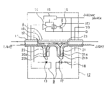
Fig. 3 is a circuit diagram showing a communication
node of an optical communication system of one embodiment of
the present invention, and Fiy. 4 is a sectional view showing
a connecting portion of a shunting light conduction path of
the communication node shown in Fig. 3.
In the figures, (11) are sections of optical fibers,
and (12) is a communication node which is the communication
system of this embodiment. This communication node ~12) is
composed of a shunting light cnduction path unit (h) and a
photo-electric conversion unit (B). (13) is a light receiving
element such as a photodiode for converting a light signal
into an electric signal, ~14) is an amplifier circuit for
amplifying the electric signal converted by the light
receiving element (13), (15) is a constant voltage source,
(16) is an outputting transistor operated by the signal from
the amplifier circuit (14). (17) is a light emitting element
such as a light emitting diode ~LED) for converting various
electrical signals into light signals, (18) is a resistor for
limitting the electric current to the light emitting element
(17). The operation of converting and amplifying the light
signal into the electric signal and the operation of
converting the electric signal into a light signal are both
carried out by the photo-electric converting unit (B) of the
communication node (12). (19) is a passing through light
conduction path in which a light signal can bidirectionally
9_
\
~ 3 ~
pass through, thereby serving as if it is a bypass path for
the light signal. (20) is a receiving light conduction path
for receiving the light signal from either directions and
having a first light receiving end (20a) and a second light
receiving end (20b). (21) is a light transmitting light
conduction path for bidirectionally transmitting the light
signals, and having a first light transmitting end (21a~ and a
second li~ht transmitting end (21b). The above-mentioned
passing light conduction path ~l9), the receiving light
conduction path (20) and the transmitting light conduction
path (~1) together constitute the shunting light conduction
path unit (A) of the communication node (12). (22) and (23)
are connecting portion with respect to the optical fibers (11)
and the shunting light conduction path unit (A). The
relationship between the optical fibers (11) and the shunting
light conduction path unit (A) is as shown in Fig. 4 from
which it is seen that the connecting portion is divided into
three systems of passing through light conduction path (19),
the receiving light conduction path (20) and the transmission
light conduction path (21).
The optical communication system of this embodiment
is constructed as above described, and is connected to the
neighbouring co~munication node stations (not shown) by an
optical fiber (11) composed of a single filament.
The operation of the communication node (12) which
is the optical communication system of this embodiment will
now be described.
For example, the description will be made as to the
case in which a light signal is transmitt~d from the station
on the left in Fig. 3. One portion of the light signal
transmitted within the optical fiber (11 ) passes through the
passing through light conduction path (19) and is transmitted
to the next right station through the optical fiber (11 ) on
the opposite side. Also, the other portion passes through the
receiving light conduction path (20~ and is transmitted to the
-10-
~ 3 ~
light receiving element (13) from the first light receiving
end (20a). Then, this signal is photo-electrically converted
by the light receiving element (13) into an electric signal,
which is amplified by the amplifier circuit (14) and is
supplied to a signal receiving input terminal RD as a
collector output through an output driver transistor (16).
On the other hand, for transmitting light, an
electric signal from a signal transmitting output terminal TD
causes the light emitting element (17) to emitt light. The
light signal photo-electrically converted by the light
emitting element (17) is transmitted from the first light
transmitting end (~1a) and the second light transmitting end
(21b) o~ the transmitting light conduction path (21) to the
right and left optical fibers (11) through both of the
connecting portions (22) and (23). Then, the signal is
transmitted to the right and left neighbouring stations.
While the description has been made as to the case
where the light signal is transmitted from the left side
station in the above embodiment, the operation is similar when
the light signal is tansmitted from the opposite side station.
Thus, the optical communication system of this
embodiment can receive a light signal from the staion on both
sides and the light signal can be transmitted to both sides.
Therefore, with this embodiment, there is no need
for forming an optical communication loop even with an optical
fiber communication formed by a single line, realizing the
bidirectional optical communication and enabling the multi-
drop bus communication.
Moreover, since one portion of the light signal is
allowed to pass through the passing through light conduction
path (19) to be bidirectionally transmitted to the station
located at the opposite sides, the light signal can be
transmitted to the next-located station even when a fault or a
power failure occurs at a station. Therefore, the light
signal can pass through the station that failed to allow the
-11-
11 3 ~
light signal to be transmitted to the next station.
Therefore, even when the communication system is
constructed with a plurality of communication nodes ~12) and
even when the light is allowed to pass through only one
station due to the light loss or the like, the communication
system can be controlled in its entirety in so far as the
neighbouring two stations do not fail. Particularly, the
probability that the neighbouring two stations fail at the
same time is extremely small as compared to the proba~ility
that only one station fails. Therefore, when the optical
communication system of this embodiment is used, the
reliability of the communication system can be significantly
increased.
Also, since the bidirectional communication is
possible in the optical communication system of this
embodiment, a communication protocol that is identical to a
conventional electric signal multi-drop bus communication
through an electric coaxial cable or the like. That is, by
installing the communication node (12) in each station of the
electric signal communication system such as of the coaxial
cable system, the bidirectional optical communication can be
easily achieved.
Further, with the above embodiment, the above-
discussed operations of shunting of the light signal, taking
out o~ the signal and the transmission of light, etc. can be
achieved by the shunt light conduction path unit (A) without
the need for using the expensive transparent prisms ~2~. The
shunt light conduction path unit (A) can be formed with
optical fibers or the like, so that the system can be made to
be inexpensive and easily made small-sized.
The description will now be made as to the
application example of the communication system of the optical
communication system of this embodiment. Fig. 5 is a circuit
diagram showing an air conditioner control system which is one
application example of the optical communication system of the
-12-
13~2~ ~9
present invention. This is a communication system in which a
plurality of communication nodes (12) described in onjunction
with Fig. 3 are connected by a single optical fiber (11). In
the figures, (11) and (12) designate the same or corresponding
components described and shown in conjunction with the
previously discussed conventional design.
In the figure, (30) is a remote controller for
regulating the air conditioner connected to the communication
node A (hereinafter referred to as A-station). Connected to
the A-station on the left is B-station and then C-station, and
D-station is connected to the right of the A-station. (313
are air conditioner indoor units connected to the B-station,
the C-station and the D-station and containing microcomputers
(32) therein. (33) is a transistor operated by the
microcomputer (32) for outputting a transmission signal to the
transmission signal output terminal TD of each communication
node (12). (34) is an electric source which may be commercial
electric source for driving each air-conditioner indoor unit
(31), (35) is an electric cell for the remote controller (30),
(36) is a microcomputer mounted within the remote controller
(30), (37) is a transistor operated by a dignal from the
microcomputer (36). (38) is a thermister mouted at the air
intake of the air-conditioner indoor unit (31) for detecting
room temperature, and (39) is an air-conditioner outdoor unit
operating in pair with each of the air-conditioner indoor
units (31)~
The control system of this air conditioner controls
the operation of three air-conditioner indoor units (31)
installe~ in a large room with intervals and connected to the
B-station, the C-station and the D-station for example by a
single remote controller (303 in accordance with the
temperature or the like. The control signal from the remote
controller (30) is converted into an optical signal in the A-
station and transmitted to the B-station and the D-station on
the both sides.
-13-
" ~3~2~1~
The communication operation in the control system
constructed as above described will now be described.
Flrstly, the microcomputer (36) operates the
transistor (37) according to the temperature signal set by the
remote controller (30) to provide an electrical signal at the
transmission signal output terminal TD of the communication
node (12). This electrical signal is photo-electrically
cvnverted by the light emitting element ~17~ within the
communication node (12) as described in conjunction with Fiy~
1. Then this signal is transmitted as a light signal from the
first transmitting end (21a) and the second transmitting end
(21b) to the B-station and the D-station located at the left
and right sides of the A-station through the optical fiber
(1 1 ) .
In the communication node (12) of the B-station,
this light signal is partially pass through the passing
through light conduction path ~19) to be immediately
tranmitted to the C-station next to the B-station. Another
part of the light signal is transmitted to the light receiving
element (13) from the light receiving end through the
receiving light conduction path (20). Then, thesignal is
converted into an electrical signal by the light receiving
element (13) and ampli~ied by the amplifier circuit (14) to be
inputt~d into the receiving signal input terminal RD. This
input signal is received by the microcomputer (32) within the
air-conditioner indoor unit (31). The microcomputer (32)
generates a pulse signal having a predetermined costant pulse
width at a predetermined communication speed in synchorization
with the received signal. The microcomputer (32) causes the
transistor (33) to operate to generate a transmission signal
in the transmission signal output terminal TD of each
communication node (12). Therea~ter, the transmission signal
is photo-electrically converted into a light signal which is
transmitted to the C-station and A-station located on the
right and left sides of the B-station through the optical
~iber (11).
Therefore, tha temperature set signal from the
remote controller (30) is transmitted also to the C-station
similarly to the case of the B-station. Moreover, the signal
is transmitted after being ampli~ied in the B-station.
Therefore, the same communication information can be
successively transmitted no matter how many s-tations are
connected next to the C-station. Since these stations have
the passing through light conduction path (19), the
communication signal from the A-station can be transmitted to
the next station even when the B-station fails or no
commercial power ~34) is connected.
On the other hand, by connecting the thermister (38)
to the input of the microcomputer (32) of the air-conditioner
indoor unit (31), the temperature data detected by the
thermister (38) can be converted into a light signal to be fed
back to the A-station.
In the A-station, the light signal is photo-
elPctrically converted and amplified to be supplied to the
microcomputer (36) of the remote controller (30). Then, by
comparing the received temperature data and the set
temperature data in the remote controller (30), the operation
conditions of a fan motor (not shown) or the air conditioner
indoor unit (39) can be suitable adjusted to achieve optimum
air conditioning.
Also, the temperature detected by the thermister
(38) of the B-station can be displayed as Z7~C , for example,
on the remote controller (30).
Thus, when the optical communication system of this
embodiment is applied, by simply connecting the plurality of
stations by the single optical fiber (11~, various optical
communications between the respective stations can be carried
outu
In the above embodiment, the communication node (12~
has been described as being an integral unit composed of the
-15-
13 L2~L19
shunt light condllction path unit (A) and the photoelectric
conversion unit (B). However, these shunt light conduction
path unit (A) and the photoelectric conversion unit (B) may be
separated.
Fig. 5 is a circuit diagram showing the
communication node of the optical communication syst0m of
another embodiment of the present invention. In this
embodiment, the shunt light conduction path unit (A) and the
photoelectric conversion unit (B) are separated as being a
light conduction path unit (12a) and a photoelectric
conversion unti (12b). In the figure, the reference numerals
(11) to (23) designate the components identical or
corresponding to the components described in conjunction with
the convention example.
In the figure, (40) is a light receiving connection
portion for connecting the first light receiving end (20a) and
the second light receiving end (20b) of the light receiving
conduction path (20) of the light conduction unit ~12a) to the
light receiving element (13) of the photoelectric conversion
unit (12b). (41) is a light transmission connection portion
for connecting the first light transmission end (21a) and the
second light transmission end (21b) of the light transmissiion
conduction path (21) of the light conduction path unit (12a)
to the light emitting element (17) of the potoelectric
conversion unit (12b).
In the communication node (12) of this embodiment,
the light conduction path unit (12a) may be connected to the
photoelectric conversion ~mit (12b) so that it has the same
construction as that of the communication node (12) of the
previous ~mbodiment and therefore the operation of the optical
communication is the same. Therefore, the optical
communication system of this embodiment can receive the light
signal from both right and left directions and can
bidirectionally transmit the light signals. Also, since one
part of the light signal passes through the passing through
-16-
~ 2~ ~9
conduction light path (19), the same advantageous results as
those of the previous embodiment can be obtained.
In particular, when the communication node (12) in
which the light conduction path unit (12a) and the
photoelectric conversion unit (12b) are separated is used, the
degree of freedom of constructing the communication system is
incxeased, allowing the user to suitably select accordin~ to
the application purpose.
While the optical communication system of the above
embodiment has been described as being applied to an air
conditioner control system, the application is not limited to
that system. For example, since the optical communication has
a feature that it is not affected by the electromagnetic
noise, it can be widely applied in various communication
industries such as information apparatus such as personal
computers, the factory communication system such as numerial
control machines, or the domestic home automation
communication systems.
As has been described, the optical shunt device of
the present invention, the section between the connecting ends
for being connected to the optical communicating optical
flbers is divided into three systems including a passing-
through light conduction path through which light signals in
two opposite directions are allowed to pass through between
the connecting ends, a receiving light conduction path having
a first light-receiving end and a second light-receiving end
each receivin~ a light signal from the connecting ends, and a
transmission light conduction path having a first light-
transmitting end and a second light-transmitting `end each
transmitting a light signal to the connecting ends, and the
light signal from the first light-receiving end and the second
light-receiving end of the receiving light conducting path is
converted into an electric signal by the light-receiving
element, ~nd this electric signal is amplified by the
amplifier circuit and converted into an optical signal by the
-1~
~31~
light-emitting element to supply the optical signal to the
first and second light-transmitting ends of the transmitting
light conduction path, so that the light signal transmitted
through the optical fiber which is a single line can be
bidirectionally received and this light signal can be photo-
electrically converted into an electric signal. Also, various
electric signal can be bidirectionally transmitted as a light
signal converted from an electric signal. Moreover, one part
of the light signal can be transmitted through the passing-
through light conduction path to the next station~ so that
even upon the fault in that particular station, the light
signal can be transmitted to the next st~tion, increasing the
reliability of the communication system. Further, the
operations of the shunting of the light signal, taking out of
the signal and light transmission can be achieved without the
need for using the transparent prism, so that the system can
be inexpensive and small-sized.
Fig. 7 is a circuit diagram showing a communication
node of an optical communication syste]n of another embodiment
of the present invention, and Fig. 8 is a sectional view
showing a connecting portion of a shunting light conduction
path of the communication node shown in Fig. 7.
In the figures, (11 l ) are sections of optical fibers
for transmitting a light signal, (112) is another optical
fiber which can be added even when the optical fibers (111 )
are connected, and (122) is a communication node which is the
communication system of this embodiment. This communication
node (122~ is composed of a shunting light cnduction path unit
(A) and an energy conversion unit or a photo-electric
conversion unit (B). (119) is a light receiving element such
as a photodiode for co~verting a light sisnal into an electric
signall (120) is an amplifier circuit for amplifying the
electric signal converted by the light receiving element
(119), (123) is a constant voltage source, (124) is an
outputting transistor operated by the signal from the
~ 3 ~
amplifier circuit (120). (121) is a light emitting element
such as a light emitting diode (LED) for converting various
electrical signals into light signals, (125) is a resistor for
limitting the electric current to the light emitting element
(121). The operation of converting and amplifying the light
signal into the electric signal and the operation of
converting the electric signal into a light signal are both
carried out by the photo-electric converting unit (B) of the
communication node (122~. ~116) is a passing through light
conduction path in which a light signal can bidirectionally
pass through, thereby serving as if it is a bypass path for
the light signal. (117) is a receiving light conduction path
for receiving the light signal from the optical fiber (112)
which can be additionally connected and the light signal in
either directions and having a first light receiving end
(117a), a second light receiving end (117b) and a third light
receiving end ~117c). ~118) is a light transmitting light
conduction path for transmitting the light signals in two
opposite directions and to the additionally connectable
optical fiber (112) and having a first light transmitting end
(118a), a second light transmitting end (118b) and a thrid
light transmitting end (118c). The above-mentioned passing
light conduetion path (116), the receiving light conduction
path (117) and the transmitting light conduction path (118)
together constitute the shunting light eonduction path unit
(A) of the communication node (122).
The reference numerals (113) and t114) are
connecting end portions with respect to the optical fibers
(111~ and the shunting light conduction path unit (A). The
relationship between the optical fibers (111 ) and the shunting
light conduction path unit (A) is as shown in Fi~. 8 from
which it is seen that the connecting portion is divided into
three systems of passing through light conduction path (11~),
the receiving light conduction path (117) and the transmission
light conduction path (118). Also, (115) is connecting end
-19-
~3~2~1~
portion with respect to the additionally connectable optical
fibers (112) and the shunting light conduction path unit (A).
The relationship between the additionally connectable optical
fibers (112) and the shuntiny light conduction path unit (A)
is as shown in Flg. g from which it is seen that the
connecting portion (115~ iS divided into two systems of the
receiving light conduction path (117) and the transmission
liyht conduction path (118).
The optical communication system of this embodiment
is constructed as above describedJ and is connected to the
neighbouring communication node stations (not shown) by the
optical fiber (111 ) composed of a single ilament, and also is
connected to the additional, third communication noide station
(not shown) by the optical flber (112) composed of a single
filament.
The operation of the communication node (122) which
is the optical shunt apparatus of this embodiment will now be
described.
For example, the description will be made as to the
case in which a light signal is transmitted from the station
on the left in Fig. 7. One portion of the light signal
transmitted within the optical fiber (111) passes through the
passing through light conduction path (116) and is transmitted
to the next right station through the optical fiber (111 ) on
the opposite side. Also, the other portion passes through the
receiving light conduction path (117) and is transmitted to
the light receiving element ~119) from the first light
receiving end (11 7a). Then, this signal is photo-electrically
converted by the light receiving element ~19) into an electric
signal, which is amplified by the amplifier circuit (120) and
is supplied to a signal receiving input terminal ~D as a
collector output through an output driver transistor (124).
On the other hand, for transmitting light, an
electric signal from a signal transmitting output terminal TD
causes the light emitting element (121) to emitt light. The
-20-
`` t~2~
light signal photo-electrically converted by the light
emitting element ~121) is transmitted from the first light
transmitting end (118a) and the second light transmitting end
(11Bb) of the transmitting light conduction path (118) to the
right and left optical fibers (111) through both of the
connecting portions (113) and (114), and also to the optical
fiber (~12) con~ected to the third communication node (not
shown) from the third light transmitting end (11 ac) . Then,
the signal is transmitted to the right and left neighbouring
stations.
While the description has been made as to the case
where the light signal is transmitted from the left side
station in the above embodiment, the operation is similar when
the light signal is tansmitted from the opposite side station.
The description will now be made as to the case
where a light signal is transmitted from the third station
connected to the additionally connectable optical fiber (112).
The light signal transmitted through the optical
fiber (112) passes through the receiving light conduction path
(117) and is transmitted from the third light receiving end
(117c) to the receiving signal input terminal RD through the
liyht receiving element (119).
On the other hand, when transmitting, the signal is
transmitted to the stations positioned right and left side as
well as the third station.
Thus, the optical shunt device of this embodiment
can receive light signals from the staions on both sides as
well as the third station ~nd the light signal can be
transmitted to both sides and to the third station.
Therefore, with this em~odiment, there is no need
for forming an optical communication loop even with an optical
fiber communication formed by a single line, realizing the
bidirectional optical communication and enabling the multi-
drop bus communication.
Further, since the connection can be established
-21-
al5o to the third station by the additionally connectable
optical fiber, a system communication in the shape of a tree
is not impossble.
Moreover, with the multi-drop bus communication by
the optical shunt device of the embodiment of the present
invention/ since one portion of the light signal is allowed to
pass through the passing through light conduction path (116)
to be bidirectionally transmitted to the station located at
the opposite sides, the light signal can be transmitted to the
next-located station even when a fault or a power failure
occurs at a station. Therefore, the light signal can pass
through the station that failed to allow the light signal to
be transmitted to the next station, and when a fault occurs in
either of the stations that station can be passed through so
that the light signal can be safely transmitted to the next
station.
Therefore, even when the communication system is
constructed with a plurality of communication nodes (122) and
even when the light is allowed to pass through only one
station due to the light loss or the like, the communication
system can be controlled in its entirety in so far as the
neighbouring two stations do not fail.
Also, when the distance between the communication
nodes (12~) is large and the light losses of the passing light
is large, as shown in Fig~ 10, the connection end portion
between the optical fibers (111) and the shunt conduction
light path unit (A), may be di~ided into four systems, two of
which being the passing through light conduction path (116),
one ~eing the receiving light conduction path (117) and the
last one being the transmitting light conduction path ~118),
thereby to increase the light energy of the passing-through
light signal, ensuring that the light signal is transmitted to
the next station.
Particularly, the probability that the neighbouring
two stations fail at th~ same time is extremely small as
-22-
~2~
.
compared to the probability that only one station fails.
Therefore, ~hen the optical communication system of this
embodiment is used, the reliability of the communicaticn
system can be significantly increased.
Also, since the bidirectional communication is
possible in the optical shunt device of this emhodiment, a
communication protocol that is identical to a conventional
electric signal multi-drop bus communication through an
electric coaxial cable or the like. That is, by installing
the communication node (12Z) in each station of the electric
signal communication system such as of the coaxial cable
system, the bidirectional optical communication can be easily
achieved.
Further, with the above embodiment, the above-
discussed operations of shunting of the light signal, taking
out of the signal and the transmission of light, etc. can be
achieved by the shunt light conduction path unit (A) without
the need for using the expensive transparent prisms (2). The
shunt light conduction path unit (A) can be formed with
optical fibers or the like, so that the system can be made to
be inexpensive and easily made small-sized.
The description will now be made as to the
application example of the communication system of the optical
shunt device of this embodiment. Fig. 11 is a circuit diagram
showing an air conditioner control system which is one
application example of the optical shunt device of the present
invention. This is a tree~shaped communication system in
which the third station is connected by a single optical fiber
(112a) to a communication system (X) in which a plurality of
communication nodes (122) described in conjunction with Fig. 7
are connected by a single optical fiber (111).
In the figure, (130) is a remote controller for
regulating the air conditioner connected to the communication
node A (h~reinafter referred to as A-station). Connected to
the A-station on the left is B-station and then C-station, D-
-23-
station and E station are connected to the right of the A-
station to constitute the communication system ~X). Also, ~-
station and G-station constitute a communciation system (Y).
It is seen that the communication systems (X) and (Y) are
generally tree-type communication systems in which the F-
station i5 additionally connected to the A-station, and the F-
station i.s additionally connected to the G-station. (131~ are
remote controllers for the air conditioning temperature
controllers each connected to the D-station. (132) is an
electric source which may be commercial electric source for
driving each air-conditioner indoor unit (130), and ~133) is
an air-conditioner outdoor unit operating in pair with each of
the air-conditioner indoor units (130). (134) is a
microcomputer contained within the remote controller (131),
and (135) is a microcomputer contained within the air
conditioner indoor unit (130).
The control system of this air conditioner is the
one in which the system (X) which controls the operation of
four air-conditioner indoor units (130) installed in a large
room with intervals therebetween and connected to the A-
station, the B-station, the C-station, the D-station and the E-
station, for example, by a single remote controller (131) in
accordance with the temperature or the like has additionally
connected thereto the system (Y) composed of the air
conditioner indoor unit (130) connected to the F-station and
the G-station so that the operation of the system can be
controlled with a single remote controller (131). The control
signal from the remote controller (131) is converted into an
optical signal in the D-station and transmitted to the A-
station, the B-station, the D-station and the E-station as
well as the additionally connected F-station and the G-
station.
The communication operation in the control system
constructed as above described will now be described.
Firstly, the microcomputer (134) uperates according
-2~-
:~ ,s~ ~ 2 ~
to the temperature sigIlal set by the remote controller (131)
to provide an electrical signal at the transmission signal
output terminal TD.
This signal is photo-electrically converted by the
light emitting element (121) within the communication node
(122) as described in conjunction with Fig. 7. Then this
signal is transmitted as a li~ht signal from the first
transmitting end (118a), the second transmitting end (118b)
and the third transmitting end (118c) (not used) to the C-
station and the E-station located at the left and right sides
of the D-station through the optical fiber (111).
In the communication node (122) of the C-station,
this light signal is partially passed through the passing
through light conduction path (116) to be immediately
tranmitted to the A-station next to the C-station. Another
part of the light signal is transmitted to the light receiving
element (119) from the light receiving end through the
receiving light conduction path (117). Then, the signal is
converted into an electrical signal by the light r~ceiving
element (119) and amplified by the amplifier circuit (120) to
be inputted into the receiving signal input terminal RD. This
input signal is received by the microcomputer (135) within the
air-conditioner indoor unit (130~. The microcomputer (135)
generates a pulse signal having a predetermined costant pulse
width at a predetermined communication speed in synchorization
with the received signal. The microcomputer (135) generates a
transmission signal in the transmission signal output terminal
TD of each communi~ation node (122). Thereafter, the
transmission signal is photo-electrically converted into a
light signal which is transmitted to the A-station and D-
station located on the right and left sides of the C-station
through the optical fiber (1i1) as well as to the F-station
through the additionally connectable optical fiber (112b).
Therefore~ the temperature set signal from the
remote controller (131~ is transmitted also to the A-station
-25 -
similarly to the case of the C-station. Moreover, the signal
is transmitted after being amplified in thecB-station.
Therefore, the same communication information can be
successively transmitted no matter how many stations are
connected next to the A-station. Also, this is also true when
the station is located at the right side of the remote
controller (D-station).
Since these stations have the passing through light
conduction path (116)l the communication signal from the C-
station can be transmitted to the next station even wh~n the D-
station fails or no commercial power (1323 is connected.
On the other hand, the F-station, to which the light
signal is transmitted from the C-station through the
additional connection optical fiber (112b), can transmit the
same communication information to the next right subsequent
stations following the G-station in the same manner as
previously described.
While the signal transmission from the C-station to
the F-station is carried out from the additional connection
end portion (15), the passing through light conduction path
(16) is not provided with respect to the signal from the D-
station (or A-station), so that no information is transmitted
to the F-station when the C-station fails. Therefore, the
stations other than the C-station, for example, the A-station
and the F-station are connected so that the communication
information can be transmitted to the F-station even when a
falut occurs in the C-station. Thus, for the similar reason
that the communication can be carried out through the passing
light conduction path B116) so far as the neighbouring two
stations do not fail, the communication information can be
transmitted to the F-station except when the C-station
connected to the F-station and the station other than the C-
station, such as the A-station, are concurrently disabled to
transmit the light signal.
As described above, in the communication node (122)
-26-
~ 3 ~ 2 A .~ ~3
of this embodiment, so far as two neighbouring stations are
not concurrently failed, the tree~configured communication
system other than the failed station can be controlled in its
entirety even when oné station is disabled due to a falut or
the like. ~lso, when it is desired to add a remote controller
Inot shown) in addition to the D-station, this addition can be
easily achieved by connecting the controller to the additional
connecting portion (115) of the E-station through an optical
fiber.
While the optical communication system of the above
embodiment has been described as being applied to an air
conditioner control system, the application is not limited to
that system. For example, since the optical communication has
a feature that it is not affected by the electromagnetic
noise, it can be widely applied in various communication
industries such as information apparatus such as personal
computers, the factory communication system such as numerial
control machines, or the domestic home automation
communication systems.
Fig. 12 is a block diagram of one example of a
control system Eor an in~ormation apparatus such as a personal
computer which is another embodiment of the present
application. In the figures, the same reference numerals as
those used in Figs. 7 to 11 designate identical or
corresponding components of the previous embodiments, so tha-t
only the di~ferences from th~ embodiment shown in fig. 11 will
be discussed with the descriptions of these components
omitted.
In this control system~ a building S and a building
T in which a network constituted by information apparatus such
as personal computers is incorporated are connected by th~
optical communication lines to construct one system. In each
bulldings S and T, an information apparatus ~140) such as a
personal computer is connected to the communication node (122)
of this embodiment, thereby constituting the communication
-27-
system. By connecting the above two systems to the previously
described additional connectab]e end portion (115), the need
for the connection by the terminals of the buildings S and T
is eliminated, and one communication system including the
buildings S and T can be constructed by connecting any
communciation nodes (122) that can be most easily connected
with the shortest distance between the buildings S and T.
For example, when it is desired to connect the
communication system within the L-shaped building S and the
communication system within the building T adjacent to the
building 5 and located at the bent portion of the "L" oE the
building S, any communication node ~122~ within the building T
is connected to the communication node (122) located close to
the corner of the "L" within the building S, and any two
stations within each of the buildings S and T are bypassed by
the additionally connectable optical fiber (112a), whereby the
communication system is obtained in which the buildings S and
T are integrally connected by the light conduction path (116)
which allows the signal to pass through and by the
additionally connectable optical ~iber (11 2b) and in which the
information communicati~n can be achieved except for the
failed station even when the communication node (122) directly
connecting the buildings S and T is failed and disabled to
transmit information.
Also, according to the combination of the optical
shunt devices of this embodiment, an unlimitted optical
connection communciation of the multi drop bus system of the
tree configuration can be realized.
As has been described, according to the optical
shunt device of the present invention, shunt light conduction
path unit connecting the optical fibers for optical
communication is divided into three systems including a
passing-through light conduction path through which light
signals are allowed to pass through, a receiving light
conduction path having a first light-receiving end and a
-28-
. ~ 3 ~ ~ t~
second light-receiving end, and a transmittiny light
conduction path having a first light-transmi-tting end and a
second light-transmitting end, and an additionally connectable
end portion is divided into two systems including the
receiving light conduction path having a third light-receiving
end and a transmitting light conduction path also having a
third light-transmitting end, and in an energy conversion
unit, the light signal from the first, second and third light-
receiving ends is converted by the light-receiving element
into an electric signal and converting this electric signal
into the light signal an electric signal after being amplified
by an amplifier circuit and further converted it into the
light signal by the light-emitting element so that it is
supplied from the optical signal to the first, second and
third light-transmitting ends of the transmitting light
conduction path, so that the light signal transmitted through
the optical fiber which is an additionally connectable single
line can be bidirectionally received and this light signal can
be photo~electrically converted into an electric signal.
Also, various electric signal can be transmitted
bidirectionally and to an additionally connectable end portion
as a light signal converted from an electric signal, so that
there is no need for forming an optical communication loop and
a single line bidirectional optical communication can be
achieved with the tree-configured communication mode.
Moreover, in the multi-drop bus mode, one part of the light
signal can be transmitted through the passing-through light
conduction path to the next station, and in the tree-
configured communication mode, by additionally connecting two
optical fibers, the light signal can be transmitted to the
next station even when a Eault occurs in that particular
station, increasing the reliabili.ty of the communication
system.
Further, the operation of the shunting of the light
signal, taking out of the signal, transmission of light and
-29--
the like can be achieved without the need for using thetransparent prism, enabling the device to become very
inexpensive and small-sized.
-30-