Note : Les descriptions sont présentées dans la langue officielle dans laquelle elles ont été soumises.
Yoss7-t)28
1~2~7
DEVICES USING HIGH TC SUPE~CONDUCTORS
AND METHOD FOR MAKING ~E SAME
Backqround o~ th~ Invention
Field of the Inv~ntion
5 This invention relates to novel d~vices and methods
for makinq thes~ devic~s usinq hiqh Tc
sup~rconductors, the superconductors exhibitinq
sup~rconductivity at temperatur~s qr~ater than 30K,
and mor~ particularl~ to substantially planar hiqh
Tc SQUID d~vices and m~thods for makin~ these
devices.
D~scription of the ~elat~d Art
Sup~rconductivity is u~ually d~fined as the compl~te
loss of electrical r~sistanc~ of a material at a
w~ll defined temp~ratur~. It is ]cnown to occur in
many materials, includinq about a quarter of the
~l~m~nts of the periodic table and ov~r 1000 alloys
and other multi-component systems. GenRrally,
superconductivity is consid~r~ to be a property of
the m~tallic state of the material since all known
superconductors ar~ m~tallic und~r the conditions
that caus~ them to bR sup~rconductinq. A f~w
normally non-m~tallic materials, for exampl~, b~come
superconductinq under very hiqh pressur~, th~
pr~ssurR convertinq them to metals b~fore th~y
~xhibit sup~rconductinq behavior.
Yoss7-02s
Superconductors are known to be very attractive for
many applications, and in particular hiqh speed
switchinq d~vices, such as Josephson type switches,
hiqh density packaqinq and circuit layouts.
Superconductors are also used in diffPrent types of
electronic instrumentation, and provide very accu-
rate and sensitive maanetic susceptometers and
maqnetometers.
While the advantaqes of superconductors are quite
obvious to scientists and enqineers, th~ common
- disadvantaqe of superconductivR materials is their
very low transitioni temperature. This temperature
is often called the critical temperature Tc, and is
the temperature above which superconductivity will
not exist. Usually, Tc is on the order of a f~w
deqrees Kelvin. For many years, the composition
havinq the hiqhest known Tc was Nb3Ge which exhibits
a Tc of ahout 23K. A revi~w of these materials i5
contained in M. R. Beasley et al, Phys. Today, 37
(10),60 (1984).
In 1986, a siqnificant technical breakthrouqh was
reported by J. G. Bednorz and K. A. Mueller in Z.
Phys. B-Condensed Matter, 64 pp. 189-193 (1986).
This was the first major improvement in the
superconductinq transition temperature in the last
decade. Th~ materials described by Bednorz and
Mueller w~r~ transition metal oxides which could
includ~ rare earth or near rare earth elements as
well as alkaline earth element substitutions. They
are layer-like crystalline structures often charac-
terized by oxyqen deficiencies. It is believ~d that
Y0987-028
~2~7
--3--
the transition metal must be multi-valent while many
choices can be made for the rare earth, near rare
earth and alkaline earth elements. Examples of such
materials include oxides in the La-Sr-Cu-0 and
Y-Ba-Cu-0 systems. Another publication further
describing these materials is J.G. Bednorz,
Europhysics Letters, 3 (3), pp. 379-385 (1987). The
class of materials first described by Bednorz and
Mueller will be hereinafter referred to as high Tc
superconductors. This is the term generally used by
those working in this field to describe these
materials, the materials being characterized as
tran~ition metal oxides having superconducting transition
temperatures greater than about 30K.
Since the pioneering work of Mueller and Bednorz, there
has been considerable technical activity to further
develop these superconductors and to provide compositions
having even higher critical transition temperatures.
Reference is made to co-pending Canadian application no.
558,109 filed February 4, 1988 and assigned to the
present assignee, describing a single phase Y-Ba-Cu-0
system exhibiting superconductivity at a temperature well
above 77K, and a method for making this composition. A
representative composition described in this co-pending
application has the formula A1M2Cu30y, where A is Y, or a
combination of Y, La, Lu, Sc or Yb; ~ is Ba, or a
combination of Ba, Sr or Ca; and y is sufficient to
satisfy the valence demands of the composition.
Y09~7-028
~ 3 ~
Further references describing these high T5
superconductors, and particularly the La-Sr-Cu-~ and
Y-Ba-Cu-0 systems are the following:
Cava et al, Phys. Rev. Le-tters, 58, 408 (1987);
Chu et al, Phys. Rev. Letters, 58, 405 (1987).
~nother significant advance in the field of high Tc
superconductors was the first report of the successful
fabrication of films of high Tc compositions and
speciically ilms belonging to the La-Sr-Cu-0 and
Y-Ba-Cu-0 systems. These films were described March 1~,
1987 at -the meeting of the American Physical Society in
New York City, and will be further detailed in a paper by
.B. Laibowitz et al submitted for publications.
The general teaching of Laibowitz et al is a vapor
deposition technical in which multiple metal sources are
used to provide vapor transport of metal atoms to a
substrate which is in an oxygen ambient. For example,
electron beam heated sources are filled with the desired
metals, e.g., La, Sr, and Cu, or Y, Ba, Cu. The rates of
evaporation are adjusted to give the nominal desired
composition at the substrate. Subsequent annealing in an
oxygen atmosphere at about 900C is used to provide the
desired stoichiometry.
These films and a more detailed description of the
fabrication process are described in a co-pending
Canadian application no. 560,149 filed February 29, 1988,
and assigned -to the present assignee.
Y0987-028
Y~
Although many scientific studies have been made
concerning these new high Tc superconductors in order to
understand -the physics and chemistry of these materials,
no one here-tofore has reported on devices and techniques
for making devices using these high Tc superconductors.
In particular, there has been no report of the successful
operation of devices comprised of these high Tc
materials, nor of techniques to make such devices having
a substantially planar structure. Generally,
superconducting devices utilize multi-layers of different
materials and have a non-planar geometry. However, some
materials, because of their polycrystalline structure,
can include grain boundaries that provide potential
barriers for the flow of electrons thereacross and can in
this way can be used as tunneling devices. Such devices
are often called boundary layer Josephson junctions, and
are described in the following references:
M. Ito et al, Japanese Journal of Applied Physics,
21 No. 6, pp L375-L376, June 1982
M. Ito et al, Appl. Phys. Lett. 43 (3), p 314,
August 1, 1983
T. Inamura et al, Japanese Journal of Applied
Physic, 21, Supplement 21-1, pp. 313-318, 1982.
Yos~7-02s
The devices described in these references occur
because of the qrain boundarles that result in the
deposited films durinq their preparat,ion. These
referenc~s do not teach a ~ay to process a deposited
film in a manner to controllably produce
superconductinq and ~onsuperconductinq reqions, and
also do not show how to make devices such as SQUIDs.
Accordinqly, it is a prlmary object of the present
invention to provide substantially planar devices
and methods for makinq these devices usin~ hiqh Tc
- - - superconductor materials.
.. ~ ...
It is another object of this invention to provide a
device that is operable at temperatures in excess of
30R and which is fabricated entirely of hiqh Tc
superconductinq materials.
It is another object of this invention to provide a
technique for controllably creatinq superconductinq,
normal and insulatinq portions in a sinqle layer or
a bulk sample of hiqh Tc superconductor.
It is another object of this invention to provide 3D
device structures in a sinqle layer of hiqh Tc
superconductinq material, and methods for makinq
these 3D devices.
It is another object of this invention to provide a
SQUID device comprised of at least one weak
superconductinq link formed in hiah Tc
superconductinq material.
YO9B7-028
It is another obiect of the present invention to
provide a DC SQUID device that successfully operates
at a temperature in excess of 60K, and methods f~r
makinq the same.
; S It is another object of this invention to provide a
SQUID device comprised of hiqh Tc superconductinq
material, the SQUID device havinq a substantially
planar confiquration and operatinq at temp~ratures
in excess of 60K.
..
~: 10: .- -It is a further object of this invention to provide
improved techniqu~s for controllably producinq
localized reqions of a hiqh Tc superconductor which
; are metallic and normal, (i.e., nonsuperconduct.ina),
or insulatinq).
It is a further object of the present invention to
provide a processinq technique for locally chan~inq
th~ properties of a hiah Tc superconductor in such a
way as to be able to create devices in the
superconductor without the requirement for usinq
different materials and/or multiple layers etc. of
; the same or different material.
BRIEF SU~ARY OF T~E INVENTION
The processinq techniques of this invention will
provide many different types of devices that are
confi~ured in a sinqle piece of hiqh Tc
superconductor that can be ~ither a film or bulk
material. These devices includ~ meander lines, Hall
structures, SQUIDS and transmission line patterns.
Y0987-028
~ ~2~ 7
In particular, a novel, substantially planar DC
SQUI~ can be fabricated in hiqh Tc material the
SQUID bein~ operable at temperatures in excess of
60K.
In the fabrication process, beams havinq sufficient
enerqy to cause damaqe in hiqh Tc superconductinq
materials are used, in order to chanqe the proper-
ties of these materials. This damaqe will, for
example, chanqe the properties of the material from
superconductinq to normal (i~e., nonsuperconductinq)
.- and even to a nonsuperconductinq insulatin~ state.
Thus, a complet~ transit.ion from crystalline to
amorphous structure can be produced in order to
leave portions of the composition superconductinq
while other portions are made insulatin~, havinq an
amorphous structure.
A particularly qood example of a beam to chanqe the
; properties of a hiqh Tc superconductor is a directed
heam of ions, such as oxyqen, As, Kr, etc. ion beams
which are directed to the hiqh Tc superconductor.
It has been discovered that these materials are
~xtremely sensitive to ion bombardment and can be
made to und~ryo chanqes in their properties where
the beam imaqes the material. It has further been
discovered t.hat the ion bomhardment technique seems
to work even more successfully as the quality of the
hiqh Tc superconductor increases. That is, where
there is a substantial amount of the superconductinq
phase present in the composition, the effect.s of th~
ion beams bPcome even more pronounc~d and it is mor~
YO987-028
1 ~ ~ 2 ~
~asy to produc~ well defin~d nonsuperconductin~
r~qions.
Jn an prefe~r~d ~mbodim~nt, this technique has been
us~d to define w~ak sup~rconductinq l-'nks in a
superconductinq loop that operates as a DC SOUID at
temp~ratur~s in exc~ss of 60~K. The weak links and
th~ superconductinq loop ar~ coplanar portions of
hi~h Tc sup~rconductinq mat~rial, while th~ sur-
roundinq portions of this material have been
rendered nonsup~rconductinq by the impinqinq ion
,,, ` r ~ ,~,~. b~am.
,
Usinq this techniqu~, many typ~s of devices and
structur~s can be creat~d, includina 3D structures
where insulatinq layers are formed between
sup~rconductinq layers, there beinq de~ices formed
in th~ superconductinq lay~rs.
Thes~ and oth~r objects, f~atures, and advantaqes
will be apparent from th~ followinq more particular
description of the preferr~d embodiments.
BRIEF DESCRIPTION OF THE DRAWINGS
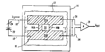
FIG. 1 is a top view of a SQUID devic~ made in
accordance with the pr~sent invention, this d~vic~
beinq comprised of weak superconductinq links formed
in a hiqh Tc superconductor, and providinq succ~ss-
ful DC S~UID operation at temp~ratur~s in ~xc~ss of
60~K.
Yoss7-02s
FIG. 2 is a side elevational view of a portion of
the s~ructure of FIG. 1 taken alonq the lin~ 2-2
thereof, and more particularly showinq some of the
superconductinq and nonsuperconductinq reaions of
material 12 in which the SQUID device i5 formed.
FIG. 3 is a schematic illustration an apparatus
suitable for providinq local modification of the
properties of hiqh Tc superconductors in order to
provide planar structures such as the SQUID of FIG~
1.
,. .
.
FIG. 4 is a voltaqe versus current plot for the
SQUID device shown in FIGs. 1, 2. This device was
measured at four different temperatures: 6, 38, 60,
77K. This plot indicates the weak link behavior of
the weak link 16A and 16B (FIG. 1), and shows the
presence of super currents at hiqh temperatures.
FIG. 5 is a plot of voltaqe versus flux modualtion
current (or flux) associated with a maqnetic field
couplinq the SQUID of FIGo 1~ and illustrates the
achievement of successful SQUID operation at three
different temperatures: 4.2~X, 28~K, and 68K.
FIG. 6 schematically illustrates a device, such as
th~ SQUID of FIG. 1, formed in a hiqh Tc
superconductor, wherein a qxound plane is also
formed in the hiqh Tc superconductor.
FIG. 7 illustrates a 3D structure comprised of two
layers of hiqh Tc superconductinq material separated
by an insulatinq layer, wherein devices can be
Yoss7-02s
~ 3! A~
11
formed in one or both of the hiah Tc superconductor
layers.
DESCRIPTION OF THE PPEFEP~ED E~BODIMEMTS
In the practice of this invention, devices are
formed in hiqh Tc superconductor materials by
impinqinq enerqy beams onto the superconductive
material in order to locally damaqe and chanqe its
properties. The material can be either a layer or
bulk material, and it can be chanqed from
-- 10 sup~rconductinq to normal (a metallic state) or from
superconductinq to an insulatinq state. The mecha-
nism for this chanqe is a damaqed - inducinq one in
which the crystalline structure of the hiqh Tc
superconductor is altered by the beam. In Appli-
cants' experimentation, it was discovered that the
sensitivity of these materials to incominq enerqy is
very hiqh, so much so that approximate 10eV per atom
of deposited enerqy is sufficient to cause a crys-
tallin~ - amorphous transition in order to chanqe
the superconductin~ metallic material to a
nonsuperconductinq insulatinq state. At a smaller
threshold, the superconductinq material can be made
to have normal properties, i.e. it is not
superconductinq, but does retains its metallic
state.
In a preferred embodiment, the beam is an ion beam,
the types of ions that can be used beinq numerous.
Thece ions include, for ex2mple, oxyqen, arsenic,
and krypton. Generally, the heavier the ion, the
Yoss7-~s
3J,.~ -t~L ~
12
mor~ damaqe that will h~ caus~d and ~.h~ l~ss the
dos~ r~quir~d to caus~ a qiv~n amount of damaqe.
It is also bPRn discov~r~d that, as the p~rcRntaqe
of th~ sup~rconductinq phas~ in t.hese hiqh Tc
mat~rials incr~ases, th~ more susc~ptible they are
to ion b~am damaq~. It appears that the pres~nce of
a conductinq s~cond phase creates reqions in t.he
hiqh Tc superconductor which are not ~asily ion
damaqed. If the amount of thesR s~cond phase
rRqions is minimal and!or if these second phas~s are
.no~t. connected, th~ superconductinq matRrial can be
bombarded to ~asily chanqe its superconductinq
prop~rties. If, however, a larqe percRntaqe of the
s~cond phase is pres~nt, it has been found that v~ry
larqe dos~s/or and heavy ions are n~c~ssary to
succc~ssfully chanqR thR propRrtiRs of thR
superconductinq material. Fortunately, as thR
quality of th~ matRrial increases so does its
abilit.y to he locally alterRd hy these ion beams.
Th~se conc~pts can be ~ore readily explained by
spRcific examplRs, such as the DC SQUID devic~ of
FIG. lo In this FIGURE a supRrconductinq SQUID,
qenerally desiqnated 10, is formed in a layer 12 of
hiqh Tc superconductinq material. Lay~r 12 is
contained in a r~friqerator 14, of a type w~ll known
in the art. Refriqerator 14 is used to maintain the
lay~r 12 at cryoqentic temperatures qreatRr than
30K. Th~ SQUID is comprised of a superconductinq
loop havinq two weak sup~rconductinq links 16A and
16P therein. These weak links are forward by
constricted portions of sup~rconductinq material.
Y~987-028
~3~2~
However, in an alternate technique, the ion beam can
b~ us~d to low~r Tc in a reqion between tWG hiqh Tc
superconductors. In this FIGURE, th~ hatchinq is
used to indicate superconductinq portions of layer
12, while the reqions of layer 12 which are not
cross hatched repr~sent reqions that are
nonsuperconductinq Pl leads 18 are ultrasonically
bonded to the superconductinq portions 20A and 20B
of the SQUID and are connecte~ to a current source
compricinq a battery 22 and a variable resistor 24.
This current source is used to provide the SQUID
. / ... bias current IB. Leads 26 are also conn~cted to
superconductinq reqions 20A and 20R and to a vo].taq~
amplifier 28 in ord~r to det~ct the voltaqe v across
the SQUID.
FIG. 2 is a side elevational view of a portion of
the SQUID device of FIG. 1, and more clearly illus-
trates th~ substantially planar superconductinq and
nonsuperconductinq reqions of the S~UID loop. Due
to the hiqh enerqy bombardment of the material 12,
portions of it will be chanqed to a
nonsuperconductinq state and, if the dosaqe is
sufficient, to an insulatinq state. For this
purpose, a patt~rned mackinq layer ~for example,
qold) is used to protect those areas of layer 12
which ar~ to remain superconductinq. Thus, portions
of layer 12 correspondinq to the weak links 16A and
16B, as well as the superconductinq loop portions
20A and 20B will be prot~cted by the mask. The
interior reqion ~0, shown as a square in FIG. 1, and
the reqions surroundinq 16A, 16B, ?nA and 20B ar~
not protected and are therefore rendered
YO987-028
14
nonsuperconductinq b~ the hiqh enerqy ion beam. In
this manner, a superconductinq loop comprisina
portions 16A and 16B, 20A and 20B will be formed
t.hrouqh the entire dept.h of layer 12. Of these
superconductinq portions, 16A and 16B are weak
superconductinq links supportinq currents therein so
that a S~UID device is created. ~s is apparent FIG.
2, this SQUID is essentially planar. When the hiqh
enerqy ion bombardment occurs, it is possible that
th~re could be dimensional chanqes in th~ areas
which are irracliated, causinq the top surface of
", lay~r 12 to vary somewhat from a completely planar
qeométry. However, such variations will be quite
small so that a substantia'ly planar structure is
formed.
In FIG. 2, it should be understood that the hiqh Tc
materials can be bulk materials or films formed on a
substrate. In these FIGURES, the substrate is not
shown, althouqh substrates such as MqO, thermally
qrown SiO2, sapphire, ~tc. can be used.
To locally alter the properti~s of the hiqh Tc
material 12, a directed heam of en~rqy is used. One
such beam is an ion h~am, which is conv~niently
provid~d by a ion beam system, systematically
illustrated in FIG. 3. In this system, an ion
source 32 provid~s a beam 34 of ions which is
d.irected to th~ hiqh Tc mat.erial 12, 1Ocated on the
subst.rate 36. It is understood that the ion source
qenerally includes an analyzinq maqnet so that the
ion beam stri~.inq the superconduct.or is comprised of
only the desired ions. The arrow 38 indicates that
v0987-028
the beam 3~ b~ scanned across different portions Oc
sup~rconductor ~2 usinq, for example, well known
electrostatic deflection means~ Th~ total ion dose,
type of ion, and enerqy of the incid~nt ions will be
illustrated for sev~ral exampl~s, to be described
later.
FIG. 4 shows the I-V curve for the SQUID Oc FIG. 1
at four tempe.ratures: 6, 38 60 and 77R. These
voltaqe-current curves show the presence of a super
current at te~peratures up to and includinq 60K.
. .. Tllis DC SQUJD actually showed a super current at
68K. The IB vs. V curve at 77K with the SQUID
immersed in liquid nitroqen had no super curr~nt but
showed a sliqht decrease in resistanc~ for IB<3~A,
which would be characteristic of a small part of the
SQUID loop beinq superconductinq, but not all of the
loop.
FIG. 5 is a plot of volta~e V across the S~UID of
FIG. 1 as a function of the current (or flux)
throuqh a coil which is used to produce a maqnetic
field that intersects t.he SQUID loop. Voltaqe
curves are shown for three different temperatures:
4.2, 28, and 68K. As is well known in the art,
th~ periodic behavior of a DC SQUID to a ramp of
maqnetic flux is a measure of the successful opera-
tion of the SQUID. As is apparent from FIG. 5, the
voltaae V across the DC SQUID is periodic wit.h the
applied maqn~tic flux (current.) at the thre~ ~ea-
sured temperatures indicatinq succ~ssful S~UID
operation. Du~ to the fact that the w~ak links 16A
and 16~ are sliqhtly different, a small asymmPtry is
YO987-028
16
appar~nt in th~ voltaq~ v~rsus flux curv~s of FIG.
5. Th~ actual curr~nt n~d~d p~r flux quantum ~
int~rs~ctinq th~ SQUID loop i9 small~r at low
t~mp~ratur~s b~cause th~ larq~ pads 20A and 20~
scr~n th~ maqnetic fi~ld from th~ pad c~nt~r and
increas~ th~ fi~ld n~ar th~ pad ~dq~s, wh~r~ th~
SQUID is located, causin~ a "flux-focussin~" ~ff~ct.
As th~ t~mp~ratur~ is incr~as~d, th~ scr~ninq of
th~ pads b~com~s w~ak~r and th~ sup~r ~ incr~as~s.
This "flux-focussinq" ~ff~ctions incr~as~s th~
maqn~tic fi~ld sensitivity of th~ SQUID by almost a
. ., r ~ ~, factor -
':
In th~ S~UID charact~riz~d ~y th~ data of FIGS. 5
and 6, th~ weak link portions 16A and 16B of th~
SQUID had width of 17 microns and a l~n~th 40
microns. The ar~a 30 was 40 X 40 microns, th~r~by
cr~atinq a sup~rconductinq loop 40 X 40 microns.
Th~ thickn~ss of the hiqh Tc superconductor 12 was
about 1 micron. Lay~r 12 was implanted by oxyq~n
ions with a dos~ of about 5 X 10¹⁵ ions/cm2, the ion
~n~rqy b~in~ about 250R~V. Superconductor 12 was a
film havinq a nominal composition YBa2Cu3Oy, wh~r~ y
is suffici~nt to satisfy th~ valanc~ commands of th~
composition. Sup~rconductivity was d~strov~d in th~
lay~r surroundinq th~ d~vic~ without actually
r~maininq r~sultinq in a planar SQUID structur~.
Normally, it would not be ~xp~ct~d that a w~ak link
havinq th~s~ dim~nsi~ns would op~rat~ as weak link.
Tt app~arC that th~r~ ~ay b~ sup~rconductinq tunn~l
junctions across th~ qrains that ar~ pr~s~nt in
th~s~ w~ak links, allowinq a Jos~phson tunn~]
Y~87-028
¢
current to pass between the reqions 20A and 20B of
the superconductinq loop. However, the present
technique can be used to mak~ very fine linewidths
for constriction weak links, especially as the
quality of the hiqh Tc materiAl increases. Thus,
the presence of barriers across ~rain boundaries is
not a necessity in order t.o provide a weak
superconductinq link in accordance with this inven-
tion.
FIGS. 6 and 7 show additional types of structures
.t.ha~ can be made by the present technique. For many
devices, it is desirable to a qround plane which is
electrically isolated from the device. This often
requires two additional layers in t.he structure.
However, this is easily accomplished in the struc-
ture of FIG. 6, in which re~ion 40 of the hiqh Tc
superconductor 42 remains superconductinq, while the
reqion 44 has been rendered nonsuperconductinq and
insulatinq ~y ion bombardment. The superconductinq
SQUID device is then formed in the top remaininq
surface of mat~rial 42, in the same manner that was
used to form the SQUID of FIG. 1. In this instance,
the ion enerqy is adjusted so that the
superconductinq properties of material 42 will be
affected only down to the top surfac~ of the insu-
latinq portion 44. Thus, cross-hatched reqions 46A
and 46B represent conductinq weak link reqions whil~
the surroundinq unshaded portions 48 have been ion
implanted and are nonsuperconductin~.
As is known in the qeneral art of ion beam implan-
tation, the enerqy of the ions determines th~ir
YC987-~?8
penetration depth into a material. This fact is
utilized to leave the bottom portion 40 of the hiqh
c superconductor in a superconductinq state, in
order to cr~ate the insulatinq reqion 44. Insulator
44 thereby provides the nec~ssary electrical isola-
; tion betw~en the SQUID device and the qround plane
~0 .
FIG. 7 shows a multilayer structure providinq a 3D
devic~ confiquration. In this structure, a first
hiqh Tc superconductor 50 has formed thereon an
; insulatinq material 52 such as, for ~xample, SiO2.
Another hiqh Tc superconductor 54 is in turn formed
on insulator 52. DevicR structures can be formed by
th~ pres~nt process in eith~r or both of th~ hiqh Tc
materials 50 and 54. Thus, weak superconductinq
links 56A and 56B are shown in layer 50, while link
weaks 58A and 58B are shown in layer 50. Addition-
ally, layer 54 includes a superconductinq qround
plane 60. In FIG. 7 the sup~rconductinq reqions of
lay~rs 50 and 52 ar~ shown with cross hatchinq,
whil~ th~ remaininq portions of these layers are
insulatinq, and therefor~ nonsuperconductinq.
FABRICATION METHODS
As was indicat~d pr~viously, ion implantation is an
effectiv~ way to provide a hiqh enerqy beam which
will chanqe the superconductinq properties of these
materials in order to r~nder portions th~reof
nonsuperconductinq~ A damaqe m~chanism is used in
which the material can be chanqed from a crystalline
to an insulatinq amorphous state. If a lesser
YO9~7-02
~C~
la
dosaqe is us~d, or if less heavy ions are us~d, the
mat~rial ca~ still remain electrically conductinq,
but ]ose its superconductlvity.
Generally, th~ techniqu~ us~s a conventionally
patter~d maskinq layer, such as qold, to prevent
the implantation of ions in reqions of the
superconductinq material where the hiqh Tc prop~rty
is to be maintained. The thickness of the mask is
chosen in accordance with the type implantinq ion
and the enerqy of that ion. Generally, the mask
thiokness is made about two-thr~ tim~s the proj~ct-
ed ranqe of the implanted ion. For exampl~, for a
250KeV oxyqen ion, a qold mask can be used havinq a
thickness of ahout 500nm. Other masks that were
used included a l~m rRsist layer on 500 nm qold
film.
Followinq implantation, any orqanic maskinq material
used to defin~ the pattern in the ion implantation
mask is removed, as by ashinq. The metal maskinq
mat~rial is then etched away by a suitable tech-
nique, such as ion millinq.
The followinq table will illustrate the successful
implantation of several hiqh Tc superconductors in
order to provide nonsuperconducting reqions therein.
In many of thes~ materials, th~ listed dosaq~ was
sufficient to cause a crystalline to amorphous
transition to occur, r~nderinq the material insulat-
inq and nonsup~rconductinq. Generally, for thes~
hi~h Tc copper oxide materials~ it has been found
that the transition to nonsuperconductinq occurs
Y0~87-028
O
with a very low ion dose, approximately 1013 oxy~en
16 ions/cm2. Howev~r, a dose 1-2 ord~rs of maqni-
tude hiqh~r is q~n~rally r~quired to mak~ th~ hi~h
Tc mat~rial very insulatinq, i.e., where the materi-
al has a sh~et resistivity qr~ater than 104
ohms/squar~.
In this tabl~, nominal compositions are pres~nted
for ~oth the Y-Ba-Cu-0 syst~m and the La-Sr-Cu-O
syst~m. Th~ column h~aded "STATE" is th~ state of
th~ implanted mat~rial. If th~ implanted material
-r~tains ItS m~tallic charact~ristic but loses its
superconductivity, its stat~ is turned "normal~,
while if the mat~rial underqo~s a more siqnificant
conversion, it will becom~ insulatinq, and los~ its
crystallin~ structur~. In one sampl~, the material
b~come hiqhly r~sistive, but not quite insulatinq,
i.R., it had a r~sistivity less than 104
ohms/square. Sample 5336A was qiven a 2-step
treatment includinq a first implantation followed by
a second implantation at a hiqher en~rqy and dosaqe.
YO987-028
TABEE
Nsmlnal Composition
S~MPLE DOSE ION ENERGY STATE Y Ba Cu O*
iontcm ,~
5332A1.5x1014 0500KeY normal 0.23 0.63 1 3.6
4X10¹⁴ 0500KeV high
~-, resistance
5328Dlx1014 Asi lMeV insul. 0.25 0.45 1 2.6
5334Clx1019 AslMeV insul. 0.30 0.76 1 5.1
5336A6X1014 lMeV As
followed by
lx1015 2.3MeV As insul. 0.43 0.46 1 4.0
; 5337E lx101 As 2.3MeV insul. 0.41 0.40 1 1.7
La Sr_ Cu _ 0
5319D lx1014 0 250KeV insul. 1.75 0.04 1 N/A
5323A 5X10¹⁵ 0 lMeV insul. ~ N/A ~ --- -
5324B 4.6x10¹⁵ 0 lMeV insul. 1.54 0.15 1 4.1
*estLmated
Y0987-028
L ~. 7
In the practice of this invention it is possible to
provide device structures using high Tc material
which would otherwise be very difficult to fabri-
cate. In particular, typical weak link configura-
tions of superconductor-insulator-superconductor
layers where the insulator is 1-2nm thick, would be
very difficult to fabricate using high Tc
superconducting oxides. Most insulating films 1-2nm
thick will crack and short out the device when
thermally cycled from room temperature up to the
900C temperatures ~re~uired to form a
superconducting oxide counter electrode. Conse-
quently, the coplanar weak link structures of the
present invention offer significant processing and
device advantages. Of course, the fabrication of
essentially coplanar structures allows for more
direct processing of subsequent layers which could
not be obtained if the SQUID were formed by tech-
niques such as ion milling, etc.
What has been described is a unique device configu-
ration comprising a high Tc SQUID and processes for
making this device~ It will be appreciated by those
of skill in the art that the type of ion chosen and
its dosage can be regulated to alter the amount of
damage produced in the high Tc material in order to
change the properties of that material. Similarly,
the energy of the accelerating ions can be adjusted
to change the depth of the deposited ions in order
to create various layers having different properties
within the same high Tc superconductor. Typically,
energies in the range 250KeV-2 or 3MeV will provide
Yo987-028
good results with these high Tc oxide
superconductors~
While the invention has been described with respect
to particular embodiments thereof, it will be
appreciated by those of skill in the art that
variations can be made therein without departing
from the spirit and scope of the present invention.
For example, the invention is intended to encompass
all high Tc superconductors of the type discovered
by Bednorz and Mueller, these materials typically
- being oxide superconductors having a layer-like
structùre and exhibi~ing Tc in excess of 30K. The
formation of these materials in both film and bulk
form has been extensively described in the litera-
ture, and the present invention can be used with anyof these materials regardless of the method by which
they are formed. Further, any type of high energy
beam can be utili2ed, as long as the beam produces
sufficient damage in the superconductor to locally
change its superconducting properties. Still
further, the beam can be used to produce a weak link
by altering the Tc of the implanted region ~having
the altered region with a lower Tc, or even in a
normal state). It is not necessary to totally
change the damaged region to an insulating states.