Note : Les descriptions sont présentées dans la langue officielle dans laquelle elles ont été soumises.
~ 321~
The present invention relate~ to the
general field o~ electric power generation and
transmission and more particularly, to a novel
conver~er for use in a High Yoltage Direct Current
S power transmission system, operating in accordance
with a pulse-width modulation principle. The
invention also extends to methods for operating the
converter.
The invention described in this
application may be considered as belonging to the
third generation Nigh Voltag~ Direct Current (HVDC~
system. The first generation is centered around the
technology of the mercury arc rectifier, the second
1~ around the thyristor. Because of the advent o~ high
power and high frequency semiconductor ~witches with
fast ~unl-o~f capabilities ~e.g. GTO's, MCT's, etc...)
the pulse-width modulatisn (PWM) technique, may be
appl~ed ~or bulk power transmission o~ the utilities.
The exploitation of the PWM ~echnique con~ti~ut~s th0
third generation ~VDC system.
Because the thyristor generatiorl o~ HVDC
ha~ been developed at considexable costs, industry is
not inclined to invest heavily on another new
teahnology if the gain~ aare merely ~arginal. ~he
invention described in t.his application not only
enable~ HVDC systems to perPorm their existing
functions better but alscl it enables ta~ks to be
performed which are not poæsible with thyristor
technology.
, . .
, - ~
~3~
Because the mercury arc recti~ier and the
thyristor cannot be turned oPf throu~h the g~te, line
commuta~ion is used~ The exi~ting convQrter sta~ion~
are desi~ned around this need of the negative halP o~
the AC voltage cycle to discontinue the conduction o~
the valve~ As a result, the present ~VDC converter
stations are inherently flawed. ~hey ar~ used because
there have been no better alternatives~ The
literature on conventiona~ HVDC is a catalog of patch
work measures to remedy thi ~atal flaw. The
: following are examples:
(i) The conventional ~YDC station is a
polluter o~ low order~ ha~monic components. The 15 harmonics are suppressed by filters which contribu~e
to a substantial fraction o~ the cost,
(ii) The conventional HVDC station cannot
operate with leading power factor and aga~n capacitors
have to b~ used when the occasion arises:
(iii) There is no active AC voltag~
support at the conventional ~DC ~tation. When th~
stat~on i~ situated in the contex~ of a weak long AC
transmission link, AC voltage collapse can occur. The
AC voltage ha~ to be supported by switched capacitors
in conjunction with static V~R controllers;
~iv) On the AC sid~, the conventional
XVDC station does not fit ænugly with the AC utility
system. This is because real power control is
achieved indirectly through controlling the phase
angle between the voltage phaser and the current
~32~.~
phaser at the AC terminals ~ The AC vol tage is not an
ac~ive voltage source. Instead, it is a voltage based
on subtractin~ the voltages acro~s the transmission
lines fro~ the active voltage~; og the generation
5 stations. As a result, the AC voltage at the
terminals change with the load current to the HVDC
station itsel~. The fit is less comPorta~le still
because the HVDC station cannot handle lealdlng power
factor. Thus in~easible operation situatiolls abound
and their occurrences have been blamed on "Voltage
Collapse";
(v3 The ¢onventional HVDC stations handle
unidirectional DC current flow only. Power reversals
are accomplished by DC voltage reversals. This is a
handicap for conventional multi terminal
conf igurations; and
(vi~ The conventional HVDC stations ~re~
20 inherenltly IIDC currerlt sources". When conv2ntior~al
HVDC stations have ko be csonrlected in a multi-terminal
configuration, patch work mea~ures have to b~ devi~ed
to make them hava the appearance o~ equivalent voltage
~ource~ Por power ~harineJ. I~ multi-term~nal
con~iguration, the conventlQnal stations can deli~er
unidire¢tional power only.
The principal object o~ the invention i
to pxovide a c:onverter system for use with a HVDC:
power transmission system, and method~ for operating
sama in order to allevi~te the shortcomings o~
conventional converter ystems operating with mercury
arc recti~iers and thyristors.
3 ~
~ ore specifically, the pxesent invention
relates ko a converter for interconnecting a first
electric network and a second electric network to
transmit electric power from one network to the other,
each o~ these networks being coupled to a respective
active power sourc~, the ~lrst network inGluding DC
link terminals for coupling thi~ ~irst network to ths
converter, there being a DC voltage having a certain
amplitude across the DC link terminals, the seco~d
network including AC link terminals for coupling this
second network to the con~erter, there being an
alternating voltage at a given substantially fixed
frequency across the AC link terminals, the
alternating voltage having an amplitudP which is
always lowex than the amplitude o~ the DC voltage,
: this ~onverter comprising:
a bridge o* valves each associated with
: an antiparallel diode, each valve of this bridge belng
capable og assuming two di~ferent states, namely an ON
state and an QFF sta~e, in the ON state th~ valve
- allowing current to pa~5 therethrough, in the OFF
state the valve blocking th~ passage of current, each
diode being no~ally rever~-biased between the DC and
alternating voltage, and thls br$dge being capabl~ o~
operating either as an in~lerter to enable transmission
o~ ~lectric power from the first network to the second
one, or a~ a rectifier to enable transmission o~
el2ctric power from the second network to the first
one;
- 30 inductor means interposed between the
bridge and the AC link tern~inals for producing a boost
voltage across the inductor means, the boost voltage
~orward-biasing the diodes to allow the same to
~3~3~
conduct electric current to thereby enable op~ratio~
o~ the bridge as an inverter and racti~ier:
capacitor means across the DC l ink
terminals, the bridge :being interposed between the
inductor and capacitor means:
valve control means coupled to the bridge
~or commanding th~ valves thereo~ to switch state to
operate the bridge as an inverter or recti~ier, the
valve control means includinq:
signal generating means for outputting a
control signal r~presentative of a desired valve ~tate
switching sequence to obtain a bridge voltage wave~orm
having a fundamental Fourier component at a frequency
corresponding substantially to the frequency o~ the
alternating voltage; and
frequency control m~ans coupled to the
signal generating means to adjust the control signal
in accordance with a drift o~ the ~requency o~ the
alternating voltage to cause the Prequency of the
~undamental Fourier component to track the ~requency
of the alternating voltag~.
In aacordance with the present invention,
there is al~o provided a converter Por i.nterconnecking
a ~irst electri~ n~twork and a ~econd electric network
~o ~ran~mit electric power ~rom on~ network to ~he
other, each of these ne!tworks being coupled to a
respective active power source9 the first network
including DC link ~erminals for coupling this first
network to the converter, the second network including
link ter~inals for coupling this second network to
the converter, there being an alternating voltage at
',,J ',)
' ' ''' ;~ .
.
~13~
a given ~u~stantially fixed frequency acros~ the ~C
link terminals, the converter cvmprising-
a ~ridge of valves, each valve o~ thisbridge being capable o~ assuming two different states,
namely an ON state and an OFF state, in the ON stake
the valve allowing current to pass therethrough, in
the OF~ state the valve blocking the passage of
current;
inductor-means between the bridge and the
AC link terminals;
capacitor means across the DC link
terminals;
valve control means coupled to the bridge
for commanding the valves thereof to switch state,
these valve control means including:
(a) signal generating means for outputting
a control 6ignal representative o~ a desire~ valve
state switching sequence to obtain a bridge ~oltage
wave~orm having a fundamental Fourier component at a
freguency corresponding substantially to the ~requency
of the alternating voltage; and
tb) ~requ~ncy control means aoupled to th~
signal generating means to adjust the control ~ignal
in accordance with a dri~t o~ the frequ~ncy o~ th~
alternatiny ~oltage to cau~e the frequency o~ the
~undamental Fourier compc~nent to track the ~requency
oi~ the alternatiny voltage, the Prequency control
means comprising a feedback circuit to generate an
error signal representative of a drift between the
frequency of the alternating voltage and th frequency
of the fundamental Fouri.er co~ponent, wherein the
frequency control means adjusts the control signal in
accordance with the errox signal to keep the fre~uency
.
13~32~
o~ the ~undamental Fourier component in synchroni~m
with the frequency o~ the alternating voltag~.
According to the invention, there is
further provided a converter for interconnecting a
first electric network and a second electric network
to transmit electric power ~rom one networ~ to the
other, each of these networks being coupled to a
respective active power source, the fir~k network
including DC link terminals for coupling this first
network to:the converter, the second network including
AC link terminals for coupling this second network to
the converter, there being an alterna~ing voltage at
a given substantially fixed frequency across the AC
link terminals, the converter comprising:
a bridge of valves, each valve of this
bridge b~ing capable of assuming two dif~erent states,
namely an ON state and an OF~ state, in the ON state
the valve allowing current to pass thexethrough, in
the OFF state the valve blocking the passage o~
current;
inductor mean~ between the bridge and the
AC link terminals;
capacit,or Jnean~ acro~s the DC link
~5 terminal ;
valve control means coupled to the bridge
for commanding the valvess thereof to switch ~tate,
theæe valve control means including:
(a) signal generating means ~or outputting
a control signal representative of a desixad valve
state switching sequence tl~ obtain a bridge voltage
wavefoxm having a fundamen~:al Fourier component at a
frequency corresponding ~ubstantially to the ~requency
o~ ~he alternative voltage; and
(b~ freguency control mean~ coupled to the
signal generating means to adjust the control signal
in accordance with a dri~t of ~he frequency of the
alternating voltage to cause the ~requency o~ the
fundamental ~ourier component to track the frequency
of the alternating voltage, wherein the valve control
means further includes memory means in which is stored
state switching sequence data for the valves of the
bridge, and first input means coupled to the memory
m~ans for receiving a si~nal representative of a
desired frequency of the fundamental Fourier
component, according to the signal rec~ived through
the ~irst input means~ the memory means outputting
state switching sequsince data allowing to obtain a
bridge voltage waveform with a fundamental Fourier
component at the desired frequency.
The present invention still ~urther
relates to a converter for in~ercon~ec~irlg ~ ~irst
electric network and a ~econd electric netwoxk ko
transmit electric power from one network to the other,
each of these networks being coupled to a respectiva
25 active power ~ource, the rir~t network inclu~ing DC
link terminals for coupling this ~irst network ~o the
converter, the second network including AC link
terminals for coupling th:is second network to the
convert~r/ there being an alternating volt~ge at a
given substantially ~ixed ~requency across the AC link
terminals, this converter c~mprising:
a bridge of valves~ each ~alve of this
bridge being capable of assuming two di~ferent states,
, D
' i , . `
q.3
namely an ON stat~ and an O~F state, i~ the ON state
the valve allow~ng current k~ pa~s therethrough, in
the OFF state the valve blocking the pa~sage o~
current;
inductor means between the bridge and the
AC link ter~inal6;
valve control means coupled to khe bridge
for commanding th~ valves thereof to switch state,
these valve control means including:
~a) signal generating means for producing
a valve state switching signal to obtain a bridge
voltage waveform having a ~undamental Fouxier
component at a certain Prequency, with a certain
amplitude and at a certain phase angle with the
alternating voltage;
(b~ memory means coupled to the ~ignal
generating means, in these memory ~eans being s~ored
control data allowing to generate diffexent valve
state switching signals, each allowing to obtain a
bridge voltage waveform with a ~undamental Fourier
component at a different ~xegu~ncy;
(c) a voltage controlled o~cillator ~or
receiving an analog ~ignal representatlve o~ ~he
de~ired ~requency o~ the ~undamental Fourier aomponent
and ~enerating in respon-~e to this analog signal an
oscillatory ~ignal representative o~ the desired
~requency;
(d) ¢ounter Imeans coupled to the voltage
controlled oscillator an~ to the memory means, the
counter means counting the oscillations of the
oscillatory signal and generating an output signal
allowing the memory mea~ls to retrieve and output
control data allowiny the 6ignal generating means to
.
. : ; . ~ .
, '' : -,.,'~ ', ,
.
generate a valve state ~witching signal to obtain ~
bridge voltage waveform wi~h a ~undamental Fourier
component at the desired ~requency.
The present invention is also concerned
with a converter or interconnecting a first eleatric
n~twork and a second electric network to transmit
elec~ric power ~rom one networ~ to the other, each of
said network~ being coupled to a respective active
power source, the first network including DC link
terminals for coupling this ~irst n~twork to the
~o~verter, the second network includ~ng AC link
terminals for coupling this second network to the
converter, there being an alternating voltage at a
given ~ubstantially fixed freguency across the AC link
terminals, the converter comprising:
a bridge of valves, each valve o~ thi~
bridge belng capable of assuming two di~ferent states,
namely and 0~ s~ate and an O~F statel in the ON state
the valve allowing current to pass thsrethrough, in
the QFY state khe valve blocking the passag~ o~'
current;
inductor means b~tween the bridge and the
AC link t~rminal~;
valve aontrol mean~ coupled to ths bridge
~or aommanding the valvels thereof ko switch state,
these valve control mean~ including:
(a) signal generating means ~or outputting
a valve ~tate switching signal to obtain a hridge
voltage waveform having a fundamental Fourier
component at a certain Prequency and at a certain
phase angle with the alternating voltage; and
(b) frequency and phas~ angle control
means coupled to the signal gen~rating means, th~e
frequency and phase angle control means including~
(i) a first signal processing circuit for
receiving a ~ignal representative of a de~ired
~requency of the fundamental Fourier component and
generating in response an output signal who5e
in~tantaneous value is representative of the voltage
angle o the fundamental Fourier component with
respect to a certain reference;
(ii) a second ignal processing circuit
having first and second inputs and an output, this
first input being coupled to the first signal
proces~ing circuit and the output to th~ signal
generating means, the ~ignal proc~ssing circuit
receiving at the second input a signal representative
of a desired phase angle between the fundament~l
Fourier component and the alternating voltage and
outputting a signal allowing the slgnal ~enerating
mean~ to produce a ~lve state ~witching signal to
obtain a bridge output waveform having a ~undamental
~ourier component at the de~ired fre~uency and at the
desixed phase anyle with th~ alternatinc3 voltage.
The present Lnvention ~urther relate~ to
a converter interconnecti.ng a ~irst electric network
and a second electric ne~work to transmit electric
power from on~ network t:o the other, each of these
networks being coupled to a respective active power
source, the ~irst network including DC link terminals
for coupling this first network to the conYerter, the
second network including AC link t~rminals ~or
coupling this second network to the converter, ther
,:,1" /. ~
2 ~ ~
be~ng an alternating voltage at a given ~ubstantially
fixed ~requency across the AC linX ter~inals, the
converter comprising:
a bridge of valves, each valve of the
bridge being capable of as uming two d~erent state~,
namely an ON state and an OFF st~te, in the ON state
the valve allowing current to pass therethrough, in
the OFF state the valve blockiny the passage of
current;
inductor means between the bridge and the
AC link terminals;
valve control means coupled to the bridge
for commanding the valves thereof to switch state, thP
valve control means including:
(a) signal generating means for outputting
a valve state switching signal to obtain a bridge
voltage waveform having a fundamental Fourier
co~ponent at a certain fr~quency and at a certain
phas~ angle with the alternating voltaye; and
(b) ~requency and pha~e angle control
means coupled to the signal generating m~ans~ the
~requency and pha~e angle control means inaluding:
~i) a ~ir~t ~ignal proce~sing aircuit ~or
receiving a si~nal rQpresentative o~ a desired
fre~lency o~ the ~undamental Fourier component and
generating in re~ponse an output signal whose
instantaneous value is representative of the phase
angle of the fundament~ll Fourisr component with
respect to a certain reference;
~ii) a second signal proc~ssing circuit
having first and second :inputs and an output, the
irst input being coupled to the first ~iynal
processing circuit and the output to the signal
,
~32 ~
generating mean~, the second ~ignal procas~ing circuit
receiving at the second input a signal representative
of a desired phase angle between the fundamental
Fourier component and the alternating voltage and
outputting a signal allowing the signal genarating
means to produce a valve state switchiny signal to
obtain a bridge voltage waveform having a undamental
Fourier component at the desired fre~uency and ~t the
desired phase angle with the alternating voltage;
wherein the frequency and pha~e angle
control m~ans further comprise~.
an adder having two inputs and an output
coupled to th~ first signal proce~sing circuit, at one
of the inputs of the adder being applied a signal
representative of a nominal frequency of the
~undamental Fourier component and at the other input
of the adder being applied a signal representative o~
a desired deviation of the frequency of the
~undamental Fourier component with respect to the
nominal frequency; and
wherein the fir~t sign~l proces~ing
circuit is ~ voltage controlled oscill~tor.
In accordance with the present invention,
there is also provided a converter i~lterconnecting a
~ir~t electric network and a second electric network
to transmit electric power from one network to the
other, each of ~hese n ~works being coupled to a
re~p2ctive active power ~ource, the ~irst network
including DC link terminals for coupling this first
network ~o the converter, t.he second nPtwork including
AC link terminals ~or coupling this second network to
the converter, there being an alternating voltage at
~3~
14
a given ~ubstantially fixed ~requency acros~ the A~
link terminals, the converter co~prising:
a bridge o~ valves, each valve of this
bridge beiny capable of assuming two different stakes,
namely an ON tate and an OFF state, in the ON state
the valve allowing current to pass therethrough, in
the OFF state the valve blocking the pa~sage o~
current;
inductor means between the bridg~ and the
AC link terminals;
valve control means coupled to the bridge
for commanding the valves thereof to switch state,
these valve control means including:
~a) signal generating means ~or outputting
1~ a valve state ~witching signal to obtain a bridge
voltage wa~efor~ having a fundamental Fouri~r
component at a certain frequency and at a certain
phase angle with the alternating voltage: and
(b) frequency and phase angle control
means coupled to the signal generating meane, ~hes~
frequency and phase angle control means including:
(i) a ~irst s.ignal proces6ing clrcuit ~or
recei.ving a signal representative oP a desired
~requency of the ~undam0ntal Fourier component and
yenerating .in response an ~utput ~ignal whose
instantaneou~ value is representative o~ the phas~
angle of the ~undamental Fourier component with
respect to a certain reference,
(ii) a second signal pro~essing circui~
having ~irst and second inputs and an output, the
first input being coupled to the firs~ signal
processing circuit and the output to the signal
generating means, the second ~ignal processing circuit
~3~ ~
receiving at the input a 61gnal representatiYe of a
d~sired phase angle between the fundamental Fourier
component and the alternating voltage and outputting
a signal allowing the signal generating means to
produce a valve state switching signal to obtain a
bridge voltage wavefor~ having a fundamental Fourier
component at the desired fre~uency and at the desired
phase angle with the alternating voltage wherein the
frequency and phasa angle control means further
comprises:
an adder with two inputs and an outputT
and
an analog-to-digital ~onverter having an
input coupled to the output of the adder and also
having an input coupled to the second input, at one of
the inputs of the adder being applied an analog signal
representative ~f a nominal phase angle b~tween the
alternating voltage and the fundamental Fourier
component, at the other input of the adder being
applied a ~ignal representative o~ a desired deviation
of the pha~e angle betw0en th~ ~undamental Fourier
component and the alternating voltage with resp~ct ~3
the nomlnal phase angle.
The present invention still further
relates to a converter iDor interconnecting a ~irst
electric network and a second electric network to
transmit electric power from one network to the other,
each of these networks b~ing coupled to a respective
active power sourceO the ~irst network including DC
link terminal.s for couplinq this first network to the
converter, the second network including AC link
terminal~ for coupling this second network to the
.,
.
3..2 ~
16
converter, there being an al~ernating voltage at a
given substantially fixed ~requency acro~ the ~C lin~
terminal~, the converter compriæing:
a bridge o~ valves, each valve o~ this
bridge being capable of a~suming twv different stat~s,
namely an ON state and an OFF ~tate, in the ON ~tate
the valve allowing current to pass therethrough, in
the OFF state the valve blocking the passage of
current;
lU inductor means between the bridge and the
AC link terminals:
valve control means coupled to the bridge
for commanding the valves thereof to switch state,
these valve control means generating a valve state
1-5 switching signal to obtain a bridg~ voltage waveform
having a fundamental Fourier component a~ a certai~
frequency, at a certain phase angle with the
alternating voltage and having a certain amplitud~,
these valve control means including:
(a) a ~requency input means for receiving
a ~ignal representativ~ ~ a desired ~requency of the
fundamental Fourier component7
(h) a pha~e angle input mean~ ~or
receiving a signal repre3entative o~ a de~ired phase
angla between the ~undamental Fourler component and
the alternating voltage; and
(c) an ~mplit.ude input means for receiving
a signal representative o~ a desired ~mplitude of the
fundamental Fourier component~ the valve co~trol means
processing the signals received at the ~requency
inputr phase angle input aJId amplitude input means and
outputting a valve state switching signal for
obtaining a bridge voltage waveform with a ~undamental
-` ~3~3~2~l~
Fourier component at the de~ired ~requency at the
desired ~hase angle with th~ alternating voltage an~
having the desired amplitude.
In accordance with the present invention,
there is also provided a conv~rter or lnterconnecting
a first electric network and a second electric network
to maintain the flow of real power from one n~twork to
the other at a predetPrmined value, each o~ these
lo networks being coupled to the respective active pow~r
source, th~ f1rst network including DC link ~erminals
for coupling the first network to the converter, t~ere
being a DC voltage having a certain amplitude across
~he DC link terminals, the second ne~work including AC
link terminals for coupling this second network to th~
converter, there being an alternating voltage at a
given fre~uency across the AC link terminals, the
alternating voltage having an amplitude which is
always lower than the amplitude of the DC voltag~, the
converter comprising:
a bridge of valves each as~ociated wlth
an antiparallel diode, each valve o~ the bridge being
capable Or assuming two di~erent states, na~ly ~n ON
state and an OFF state, in the ON tate ~he valve
allowing current to pass therethrough, in the O~F
state the valve blocking tha passaye o~ current, each
dlode being normally reverse-biased between the DC and
alternating voltage, and the bridge being capable o~
operating either as an inverter to enable transmission
of electric power Prom the first nstwork to ~he second
one, or as a rectifier to enable transmission of
~lectric power from the second network to the first
one;
: .
~L3~3~
18
inductor means interposed between the
bridge and the AC link terminals for producing a boo~t
voltaqe across the inductor means, the boost voltage
forwar~-biasing the diodes to allQw the sams to
conduct electric ~urrent to thereby enable operation
of the bridge as an inverter and rectiPier;
capacitor mean~ across the DC link
terminals, the bridge interposed b~tween the inductor
and capacitor means, the capacitor means for ~13
maintaining a DC voltage across the bridge greater
than an absolute value of the alternating voltage, and
(2) filtering out switching ripples occurring at the
DC link terminals:
valve control means coupled to the bridge
to command the valves thereo~ to switch state to
operate the bridge as an inverter or recti~ier and, ~o
obtain a bridge voltage waveform with a fundamental
Fourier component having a ~requency cvrresponding
substantially to the ~requency of the alternating
voltage, the valve conkrol means in~luding a phase
angle input means ~or receiving a phase angle signal
representative of a des.ired phase angl0 between the
Pundamental Fourier component and the alternating
voltage, in respon~e to the phase ang:le æignal the
valve control mean~ vutputting a valve state swltching
~ignal to obtain a bridg,e voltage wave~orm having a
fundamental Fourier component at the desired phase
angle with the alternatinc~ voltage, substantially to
the frequency of the alternating voltage, the valve
control means including a phase angle input means for
receiving a phase angle signal representative o~ a
desired phase angle between the fundamental Fourier
component and the alternating voltaye, in response to
. ~';
'' :
~1 3~ 3~
19
the pha~e angle ~ignal the valve control mean~
outputting a valve ~tate ~witching signal to obtain a
bridge voltage waveform having a fundamental Fourier
component at the desired phase angle with the
5 alternating voltage:
a signal processing circuit coupled to the
phase angle input means, this signal processing
circuit outputting the phase angle signal;
feedback means coupled to the signal
processing circuit, this feedback means producing an
error signal repr~sentative o~ a difference between
the amount of real power flowing through the converter
and the predetermined value, the signal processing
means receiving the error signal and altering the
phase angle signal in accordance with the error signal
allowing to obtain a bridge voltage waveform ~ith a
fundamental Fourier component at a phase angle with
the alternating voltage corresponding t~ a real power
flow through the converter at the predete~mined value.
The present invention is further aoncerned
with a converter ~or interconneating a fir~t electrl~
network and a second electric network to m~intain the
~low of real power ~rom one network to the other at a
predetermined value, each o~ these networks being
coupled to a respective active powar æource, the ~irst
network including ~C link terminals ~or coupling this
~irst network to the converter, the second network
including AC link terminals ~or c~upling this second
network to the converter~ there being an alternating
voltage at a given fre~.lency across the AC link
terminals, the converter comprising:
.
~3~3~
7,0
a bridge o~ valYes, each valve o~ this
bridge being capable of assuming two di~ferent states,
namely an ON state and an OFF state, in the ON state
the v~lve allowing current ko pass therethrough, in
the OFP state the valve blocking the passage o~
current;
inductor means between the bridge and the
AC link terminals:
valve control means coupled to the bridge
to command the valves thereof to switch state to
obtain a bridge voltage waveform with a fundamental
Fourier component having a frequency corresponding
su~tantially to the ~requency of the alternating
voltage, the valve control means including a phase
angle input means for receiving a phase angle signal
representative of a desired phase angle between the
fundamental Fourier component and the alternating
voltage, in responsa to the phase angle æignal the
valve control means outputting a valve state ~witching
signal to obtain a bridge voltage wave~orm having a
fundamental Fourier component at the desired pha~e
angle with the alternating voltage;
a ~ignal processing clrcuit coupled to th~
phase angle input means, these ~ignal pro¢eedi.ng5 aircuit outputting the phase angle signal;
feedback mea~ns coupled to the signal
prooeedin~ circuit, these feedbacX means producing an
error signal representati.ve of a difference between
the amount o~ raal power flowing through the converter
and the predetermined value, the ~ignal processing
means receiving the error signal and altering the
phase angle ~ignal in accordance with the ~rror signal
allow.ing to obtain a bridge voltage waveform with a
., I
~313~
21
fundamental Fourier component at a phase angle with
the alternating voltage corresponding to a real power
flow through the conv~rter at the predetermined value;
wherein the signal processing circuit
includes:
~ a) means responsive to the error ~ignal
to generate a frequency drift error signal indicativ~
of a d.ri~t between the frequency of the fundamental
Fourier component and the ~requency of the alternating
voltage; and
(b) means responsive to the frequency
drift error signal to alter the phase anyle signal for
maintaining the frequency of the ~undamental Fourier
component in synchronism with the frequency of the
1~ alternating voltage.
The invention is still further concerned
- with a converter for interconnecting a first electric
network and a second electric network to maint~in the
~low of real power ~rom one network to the other at a
predetermined value, each of these networks being
coupled to a respective active power source, khe first
networX including DC link terminal~ Por couplillg khi~
~irst network to the converter, the second network
including AC link terminals for coupling this second
network to the converter, there being an al~ernating
voltage at a given frelquency across the AC link
terminals, the converter ~omprising:
a bridge of valves, each valve of this
bridge being capable of assuming two different state~,
namely an ON ~tate an~ an OFF state, in the ON ~tate
the valve allowing currenk to pass therethrough, in
'f i ' ~
, ;'/"''
~ 3 ~
22
the OFF state the valve blocking the passage of
current;
inductor means b~tween the bridge and the
AC lin~ terminals;
valve control means coupled to the bridge
to command the valves thereof to ~witch state to
obtain a bridge voltage waveform with a fundamental
Fourier component having a Prequency corresponding
substantially to the frequency of the alternating
voltage, the valve control m~ans including a phase
angle input means for receiving a phase angle ~igna}
representa~ive ;of a desired phase angle between the
fundamental Fourisr compon~nt and the alternating
voltage; in response to the phase angle signal the
1~ valve control means outputting a valve ~tate ~witching
signal to obtain a bridge voltage wave~o~m having a
fundamental Fourier component at the desirad phase
angl~ with the alternating voltage7
a signal processing circuit coupled to the
pha~e angla input mean~, this signal proce~sing
circuit outputting the phase angle ~igna}:
Eeedback m~ans coupled to the slgnal
processing clrcult, this ~eedback means produc~ng an
error signal representative o~ a di~erence between
the amount of real power ~lowiny through the converter
and the predetermined vallue, the signal processing
means receiving the error ~i~nal and altering the
phas~ angle ~ignal in accordance with the error signal
allowing to obtain a bridge voltage waveform with a
fundamental Fourier compon2nt at a phase angle with
the alternating voltage corresponding to a real power
flow through the converter at the pradetermined value
wherein the feedbac~ means in~ludes:
~3~2:~
23
girst mean~ for producing a slgnal
representative of the amount of real power ~lowing
through the converter;
second means for producing a signal
repre~entative of the predetermined value;
third means coupled to the ~irst and
secon~ means for processing the signal representative
of the amount of real power flowing through the
converter and the signal representative o~ the
predetermined value, and outputting th error signal;
and
wherein the signal processing circuit
includes:
fourth means for generating a signal
representative of a nominal frequency o~ the
fundamental Fourier component;
~ ifth ~eans coupled to the fourth means
and to the third means, these ~ifth means prccessing
the signal representative of a nominal ~requency o~
ths ~undamental Fourier component and the error
signal, and outputting the ~requency dri~t error
siqnal.
The present still ~urther rela~es to a
converter ~or interconnectiny a ~irst electria network
and a ~econd electric n~.twork to transmit electric
power ~rom one network t~D the other, each oi th~se
networks being coupled to a respective active power
source, the first network including DC link ~erminals
~or coupling this first network to the converter~ the
second network including AC link terminals ~or
coupling the second network to the convert~r, there
being an alternating voltage at a given ~requency
~3~32~
2~
al-ross the AC linX terminals~ the converter
maintaining a voltage acros~; th~ DC link terminals at
a predetermined value, the converter comprising:
a bridge of valves, each valve of the
bridge being capable of ~ssuming two di~feren~ state~,
namely an ON state and an O~F state, in the ON state
the valve allowing current to pa~s therethrough, in
the OFF state the valve blocking the passage of
current:
inductor means between the bridge and the
AC link terminals;
valve control means coupled to the bridge
to command the valves thereo~ to switch state to
obtain a bridge voltage waveform with a fundamental
Fourier component having a frequency corresponding
substantially to the frequency o~ the al~ernating
voltage, the valve control means including a phase
angle input means for receiving a pha 0 angle signal
representative o~ a desired phase angle between the
~undamental ~ourier component and the alt~rnaking
voltage, in respon~e to the phase angle signal the
valve control means outputting a valve state ~witching
signal to obtain a bridge voltaye wave~orm havlng a
~undamental Fourier compon~nt at the desired pha~e5 angle with the alternating voltage;
a signal proces~ing circuit coupled to the
phase angle input means) this signal processi~g
circuit outputting the pha~se angle signal;
feedback mean~ coupled to ~he signal
processing circuit, these ~e2dback means producing an
error signal reprasentativ~! of a di~ference between
the voltage across the DC lin~ terminal~ and the
predetermined value, the signal processing means
13~3~
receiving the error signal and altering the phase
angle signal in accordance with the error signal
allowing to obtain a bridge voltage wa~eform with a
funda~ental Fourier component at a phase angle with
the alternating voltage corresponding to a voltage
acro~s the DC link terminals ~t the predet~rmined
value.
The invention is also concerned with a
converter for in~erconnecting a first electric network
~nd a second electric network to transmit electric
power from one network to the other, each of these
networks being coupled to a respective active power
source, the first network including DC link terminal~
for coupling this first network to th~ converter, the
~econd network including AC link terminals ~or
coupling the second network to the converter, there
being an alternating voltage at a given frequency
across the AC link terminals, the ~onverter
maint~ining a voltage acro~s the DC llnk terminal~ at
a predetermined value, the converter comprising:
a bridge o~ valv~s, eaah valve o~ thi~
bridge being capabl2 o~ assuming two di~erent ~tate~,
namely an ON ~tate and an OF~ state, in the ON ~tate
the valve allowing current ~o pass therethrough; in
the OFF state the valv~ blocking the passage o~
current;
inductor means between the bridge and the
AC lin~ terminals;
valve control ~eans coupled to the bridge
to command th~ valves thl2reof to switch ~tate to
obtain a bridge voltage wave~orm with a fundamental
Fourier component having ~ frequency corresponding
~3~3~
26
substantially to the ~requency of ~he alternating
voltage, the valve contrvl ~eans including a phase
angle input means for receiving a phase angle signal
representative of a desired phase angle between the
fundamental Fourier component and th~ alternating
voltage, in response to the phase angle signal the
valve control means outputting a valve state switching
signal to obtain a bridge voltage waveform having a
~undamental Fourier component at the desired phase
angle with the alternating voltage;
signal proces~ing circuit coupled to the
phase angle input m~ans, the signal processing circuit
- outputting the phase angle signal;
feedback mean~ coupled to the fii~nal
processing circuit, the feedback mean~ producing an
error signal r~presentative of a dif~erence between
the voltage across the DC link terminal~ and the
predetermined value, the signal processing mean~
receiving the error signal and altering the phase
angle signal in accordance with the error aignal
allowing to obtain a bridge voltage wave~or~ with a
~undamental Fourier component at a pha~e angle with
said alternating voltage correspondiny to a voltage
across the DC link terminals at the predetermined
valua wherein the ~ignal processing circuit includes:
means responl~ive to the error signal to
- generate a ~requency drift error signal indicative of
a dri~t between the frequency ~or the fundamental
Fo~ier c~mponent and the ~requency of the alternating
voltage;
means re~ponsiv~ to the freguency dri~t
error signal to alter khe phase angle signal ~or
maintaining the frequency o~ the ~undamental Fourier
.
:' ' '
~L3~3~
27
component in synchronism with the frequency o~ the
alternating voltage.
According tQ the invention, in
combination:
a positive DC bus;
a negative DC bus;
a first electric nekwork coupled to an
active power ~ource, this first electric network
including AC link terminals, there b2ing an
alternating voltage across the AC link terminals;
a second electric network coupled to an
active power source, this second electric network
including AC link terminals, there being an
alternating voltage across the AC link terminals of
the second electric network;
a ~irst converter coupled to the AC link
terminals of the first network, this ~irst convert~r
including DC link terminals coupled to the buses;
a second convert¢r coupled to the AC link
terminal~ of the ~econd network, the second conv~rter
including DC li.nk terminals coupled to the bu~es, each
converter includlng;
(a) a bridge ~ valves, each valve o~ this
bridge being capable of as~uming two di~ferent states~
namely an ON state and on OFF state, ln the ON state
the valve allowing current to pass therethrough~ in
the OFF state the valve blocking the passage o~
current;
(b) inductor me~ans between the bridge and
the AC link terminal~ o~ the network coupled to the
converter;
. ~
i .
~ ' '' '' ' ',
1~32~
~ c) valve control means ~oupled to the
bridge for commanding the valve~ thereo~ ~o switch
state to obtain a bridge voltage wave~orm having a
~undamental Fourier component ak a certain ~requency
and at a certain phase angle with the alternating
voltage at the AC link terminals of the network
: coupled to the converter, the valve control means
including a phase angle input means ~or receiving a
signal representative of a desired phase angle between
ths ~undamental Fourier component and the alternating
: voltage at the AC link kerminals of t~e~ netwoxk
coupled to the converter, in response to the sig~al
received through the phase angle input means the valve
control means g~nerating a valve state switching
signal to obtain a ~undamental Fouri~r co~ponent at
the desired phase angle with the alternating voltage
at the AC link terminals of the network coupled to the
converter;
a first signal proce~sing circuit coupled
to the phase angle input means o~ the valve control
means of the fir~t converter, the ~irst ~ignal
processing ~ircuit generatin~ a signal to contxol th~
pha~e angle between the ~undamental Fourier aomponent
o~ the ~ir~t converter ~nd the alterrlating voltage at
th~ AC link terminals o~ t:he ~ir~t network to maintain
the voltage across the DC link terminal~ of the fir~t
converter generally Gonstant; and
second signal processing circuit coupled
to the phase angle input means o~ the valv~ control
means o~ ~he second converter, the second signal
processing circuit generating a signal to control the
phase angle between the ~undamental Fourier component
o~ the second converter and the alternating voltage at
., ~, .. . .
~ ~32~
29
the AC link terminal~ of the second nstwork ko
maintain the amount o~ real power ~lowing through the
second converter at a predetermined level.
Also in accordance with the present
invention, in a converter for interconnecting a ~irst
electric network and a second electric network to
transmit electric power from one network to the other,
each of these networks being coupled to a respective
actiYe power source, the first network including DC
link terminal or coupling this ~irst network to the
converter, the second network including AC link
terminals for coupling this second network to the
converter, there being an alternating voltage at a
~iven fr~quency across the AC link terminals, the
converter comprising:
a bridge of valves, each valve of this
bridge being capable of assuming two dif~erent ~tat~s,
namely and ON state and an OFF state, in the ON state
the valve allowing current to pas~ therethrough, in
the OFF state the valve block~ng the pa~sage o~
current;
inductor means between the bridge and the
AC link terminal~;
valve oontrol means coupled to the bridge
t~ co~mand the valve~ t,.hereo~ to switch state to
obtain a bridge voltage waveform with a *undamental
~ourier componsnt having a frequency corresponding
substantially to the frequency of the alternating
voltage, the valve control means including a phase
angle input ~eans for receiving a phase angle signal
representative of a desired phase angle between the
fundamental Fourier component and the alternating
: . . '~: . .
, :: ,. ,
', ~ `
~3~3~
voltage, in response to the phase angle signal the
valve control m~an~ outputting a valve state ~witchlng
signal to obtain a bridge voltage waveorm having a
Xundamental Fourier compo-nent at the desired pha~e
anqle with the alternating voltage;
a process for controlling the amount o~
real power flowing thr~ugh the converter, thi~ process
comprising the step of:
varying the phase angle signal to bring
the amount of real power ~lowing through the converter
at a desired value.
In accordance with the present invention,
in a converter for interconnecting a f$rs~ electric
network and a second electric network to transmit
electric power fro~ one network to the other, each o~
these networks being coupled to a respectiY~ active
power -source, the first network including DC link
terminals for coupling thi first network to the
co~verter, the second network including AC link
terminals for coupling thi~ seaond network to the
converter, there being an alt~r~at~ng voltage at ~
given frequ~ncy acros~ the AC link term.inals, the
converker compri~ing;
a bridge of valves, each valve o~ thi~
bridge being capable oX assuming two diX~eren~ ~tate~,
namely an ON state and an OF~ state, in the ON ~tate
the valve allowing current to pa~s therethrough, in
the O~F state the valve blocking the passage of0 current;
inductor means bekween the bridge and the
AC link terminals;
~3~1 32~
31
valve control mean~ coupled to the bridge
to command the valve~ thereof to switch state to
obtain a bridge voltage waveform wlth a ~undamental
Fourier component having a ~requency corresponding
~ubstantially to the *xequency of the alternating
voltage, the valve control means including a phase
angle input means for receiving a phase angle ignal
representative o~ a desired phase angle between the
~undamental Fourier component and the alternating
voltage, in response to the phase angle signal the
valve control means outputting a valve state switc~ing
signal to obtain a bridge voltage waveform having a
fundamental Fourier component at ~he desired phase
angle with the alternating voltage;
a process for controlling the Yoltage
across the DC link terminal~, the process compri~ing
the step of:
- varying the pha~e angle signal ~o bring
the voltage across the DC link terminals to a desired
value.
The converter, according to the invention,
basically serves as ~ link between two n~twork~ ~or
power transmi~6ion in bulk o~ the utiliti~s and
~5 advantageou~ly UBe~ an array o~ ~emiconductor switch
devices wlth turn-o~ caLpabilitie~ other than lina
commutation, such as gate turn-o~ capabilities or
forced commutation, among others.
This basic structure permits to implsment
strategies to control the c~onverter according to a P~M
principle to achieve an added degree of ~reedom in
control which overcomes many of the well known
~ 3 ~
objec~$ons and limitations o~ existing conv~rter
stations.
The PWM converter according to the
S invention ~ay be used to perform at least one of the
~ollowing tasks:
(a) a voltage angle control;
(b) voltage amplitude control;
(c~ power ~low control:
(d) VAR control;
(e) stability and dynamic performance
e~hancement; and
(~ multi-terminal HVDC transmission.
1~
For the purpose o~ briefly illustrating
the invention, examples o~ PWM converter~ will be
given hereinafter, per~orming the above listed
~unctions. However, this brie~ descrlption hould not
be interpreted in a limiting manner because v~riation~
are possible without departing ~rom the spirit o~ ~he
invention.
(~) Voltage Angle Control
In a conventional AC transmission
pxactice, real power is comtrollad through the voltage
angle and reactive power through the voltage
amplitude. Strictly speaking, the r2al and reactive
pow~rs are not decoupled. The conventional practice
is adopted here as a rsugh rule of the thumb. In
generation stations, both the voltage angle control
and the voltage amplitude control are provid~d by the
: :
`` ~ 3 ~
33
speed governor control and the Pield excitation
control respectlvely~
The PWM converter, according to ~he
invention, has the same AC voltage angle control over
the real power and AC voltage amplitude control over
the reactive power. Thus, the PWM converter has the
same control attributes as the generator stations and
n~eds not be treated as a special case in load flow
studies. ~urthermore, since the PWN converter
operates with semiconductor switches, it is e~pected
to have faster time response than a generator station
where long time constantæ, associated with the
governor control and ~ield excitation control, are
present.
With the PWM converter, according to ~he
invention, the voltage angle may be changed indirectly
by time integrat~on of the input ~requency or directly
by adding or subtracting a designated angle.
'rhe PWM converter has two input~ ~or it~
voltage angle control:
(1) a ~requency control input by which
indireat voltage angle control ie achieved by
integration o~ the ~requency command signal; and
~ 2) a volt.age angle con~rol input by
which the direct voltage angle control i~ achieved.
The ~requency control input is an analog
voltage applied to a Voltage Controlled Oscillator
~VCO) whose pul~e rate i~ proportional to the input
voltage. The pulseæ are counted by binary counterO
~ ~ 3 ~
34
The aounting corresponds to integration o~ the
frequency. The in~tanta~eous value o~ khç counter
output is repr~sentative o~ the voltage angle which,
thus, is indirectly controlled through the ~raguency
control input~
The voltage angle control input wh~ch is
the direct angle control, is an analog signal first
converted by an analog-to-di~ital (A/D) converter to
: 10 a bina~y number. A binaxy adder su~s this binary
nu~ber with the binary number outputted by the binary
counter. The sum is then used as an address to an
erasable-programmable read only memory (EPROM~ which
serves as look-up tables~ The look-up tables con~ain
the discretized values of sinusoidal waveforms,
constitu~ing modulating signals, and a triangular
wavefo~m, constituting a carrier signal.
As the VCo keep~ pulse~, th~ look-up
tables are ~canned 80 that the sinusoidal modulating
wavefsrms and the triangular carrier wave~orm are
reconstituked by digital~to-analog (D/A) aonver~ers,
semiconduckor swikches o~ the PWM convert0r being
tr~ggered at the intersections o~ the modulating
wave~orm and the carrier wave~orm.
~ rha pulse rate of the VC0 determina3 the
frequency vf the voltage output Q~ the PWM converter.
Th VC0 can also control indir~ctly the voltagP angle
with respect to a fixed fr quency re~erence. This i~
done by "jogging" the fre~uency control. To advance
the voltage angle, the! frequency is increased
momentarily ~rom the ~ixe~ referenceO To retard the
,
.
~3~
voltage angle, the frequency i8 decrea~ed momentarily
~rom the ~ixed reference.
The direct voltage angle control simply
adds or ~ubtracts the desired angle without passing
through the frsquency control.
Wi~h the PWM converter, according to the
invention, real power may be controlled by adjusting
the voltage angle. This con~orms to the practice of
real power control in generator stations.
It is by retarding or advancing the
voltage angle of the PWM converter, with respect to
that of ~he AC utility system to which it has been
synchronized, that the converter is ~ade to operate as
a rectifier or an inventor.
(B) AC Voltage Amplitude Control
In a PWM converter, control of thQ voltagQ
amplitude is highly desirable in order to aahieve
control ov~r the reactlve power ~lowing through the
convert~r or to maintain the voltage amplitude
25 conMtant at the AC ~ide of the ~onverter.
To keep the AC voltage constant/ the
amplitude o~ the ~unda~men~al Fourier harmonic
component o~ the AC voltage is maintained con~tant in
spite of minor variation~ o~ the voltage in th~ DC
link. Such voltage fluctllations are mainly: due to
load variation~ because o~ the vvltage drop at the DC
lines due to their resistivity. Since in a XVDC
~L3~2~ ~
36
converter, the AC voltage is ~uppor~ed by ~he DC
voltage, such fluctuations are reflected on the AC
side.
To compen~ate for possible DC voltage
variations, the PWM converter, according to the
invention, is provided with a feedback loop to measure
the DC voltage and compensate for its variation~ by
adjusting accordingly the amplitude of the fundamental
Fourier harmonic component at the AC side of the
converter.
With a conventional conYerter, an AC
voltage regulator would have been used. This would
have consisted of measuring the AC voltage amplitude t
comparing it with the desired reference and applying
the error signal in a feedback loop to a voltag~
~mplitude control.
The advantage ~ the invention is that the
converter 15 not encumber2d by an unnecessaxy ~eedbaak
loop. This ~rees the vol~age amplitude control ~or
axecution o~ other tasks suah a~: (1) react,ive power
control ~nd ~) stability and dynamic performance
enhancement.
In ord~r t~ maintain the DC voltaga
con~tant across the DC link capa¢itor, the PWM
converter must rec~ify (or invert~ the right amount o~
AC power so as to balance the DC power leaving (or
entering) the DC link ten;ninal~ in order to prevent
the charge and he~ce the ~oltage across the DC link
capacitor ~rom changing. In consequence, there is at
:
,~' ..
~3~36~ ~
37
leas one PWM converter where the DC voltage is
maintained constant, designated hereina~ter as "master
DC voltage regulator" and it i5 basically a pOW8X
slack and ensures that the power balance of the DC
network can be maintained.
Maintaining the power flow through the PWM
converter may be achieved:throuyh a frequency and a
voltage angle lock loop, as it will be explained in
~0 detail in the next section.
From the above, it appears that a PW~
converter is an active voltage controller and this
con~rasts favourably against the passiveness of the
conventional line commutated converters. Viewing the
~undamental ~ouxier series component o~ vol~ages at
the AC terminals of the PWM conYerter as e~uivalent AC
voltage sources, the three attribute~ of the AC
voltage are directly controllableO
(1) the amplitude;
(2) the frequency; and
. (3) the voltage phase angle.
The direct control over these three
attributes enables the PWM converter to have a
significant role to play in matching load flow
requir~ments in damping intar-system oscillations and
in ~tabilizing the power pool.
(C) Power Fl~w Control
1313?J:19
38
Power ~low through a PWM converkQr can be
controlled by ad~usting the voltage angle. A PW~
converter whose task is mainly to control th~ xe~l
power ~low therethrough i~ designated her~inafter as
"power di~patcher".
There are several ways o~ measuring the
real power: AC wattmeter, DC wattmeter, or DC link
current (as~uming that the DC link voltage i~ held
constant). The measured power is ~ompared to the
pow~r assignment and the error is applied to the
fre~uency control and the direct voltage control of
the voltage angle controller in a negative feedback
loop. The power assignment may be for positive power
15 (rec~ifier) or for negative power (inverter). The
voltage angle controller will adjust the voltage angle
with respect to the res~ o~ the AC s~s~em until th~
assigned power is delivered. The assigned power i5
maintained in spite of: ~1) the fre~uency drifts t2)
the circuit topology changes arising from changes in
unit commitment and (3) load ~low change8 of the ~C
utility system~
Whether the PW~ converter operate~ a~ a
power di~patcher or a~ a master DC voltaye regulator,
prererably the volta~e angle control i5 exclusively
employed to maintain the assigned power or the slaak
power~ The voltage amplitude control may then b~ used
for stabili~y and dynamic performance enhancement.
(~ VAR Control
~'
' ' ~ ' ~ , .
; ''" , '~' .: '
.,
~L3~3'~ ~
39
The power dispatcher and~or the master DC
voltage regulator op~rating with ourrent phase angles
ranging ~xo~ 0 to 360, are themselves statis ~R
controllers provided the current ratings of the
converters are suf~icient. .While the assigned real
power or slacX power is delivered, the reactive power
is automatically handled by the station provided the
MVA ratinq is high enough. Switched capacitors and
inductance~ can also be used which are placed in
parallel at khe AC terminals of the power di~patchers
and/or the master DC voltage regulators for the
purpose of reducing the MV~ ratings of the converters
and hence th~ overall costs. A PWM converter station
is rated to control static V~Rs within a limited
range. The station is equipped with tran~ducers which
measure VAR~. As the upper limit o.~ the ~AR range es
exceeded, a capacitor is switched ON. Alt~rnatively
when the lower limit is reached, a~ capaci~or is
; switched OFF. When all the capacitors in ths bank
have been switched OFF, an inductance from the
inductor bank i5 switched ON.
The ~witched capacitors and/or switched
inductor~ control th~ V~Rs in quantum ~tep~ Between
any two quantum ~tep8, the continuous adjust~ent o~
the VARs is provided by the PWM converter. Thi~ would
normally have to he pr~vided by SVC ~Static VAR
controllers3 in conventional converter stations.
tE) Stability and Dynamic Performance Enhancement
An interconnec!~ed system consisting of one
or several ~C systems integrated together by a DC
~3~3~
network con~isting of two or ~ore PWM converters may
have eigen-modes which are lightly da~ped or eigen-
~ode~ which are on the verge of instability.
In many cases, by pole shifting technique~
or by other well-known methods of control~ the lightly
damped or marginal stable mo~es can be madP to have
improved damped response provided control leverages
exist ~or introducing the control feedback signals.
A PWM converter offers 3 levers of control for
stability and dynamic performance enhancemant~
voltage amplitude control, (2) ~requency control (3)
direct voltage angle control.
In both the power dispatcher and the
~aster DC voltage regulator ~odes, the frequency
control and the voltage angl~ control have been u~ed
in a frequency and voltage angle lock-~oop to track
the power as~ignment or the DC vsltage reference~
Nevertheless, bvth the frequency control and the
voltage angle control can ~till be used with ~eedbac~
loops for stability and dynamic per~o~mance
enhancement, if neceesary.
In both the power dispatcher and the
master DC voltag~ regulator mode~, the voltage
amplitude control has been deliberately le~t
unencumbered o~ specific duties requiring feedback
loops~ The intent is tG dedicate this control for
~tabil}ty and dyna~ic perP~rmance enhancement.
In a PWM converter, in accordance with ~he
invention, the three controllers: voltage amplitude,
:. '
-' ", ' , ' '
.. ,, : I
32~
~1
frequency and voltage angl~, can be used in
con~unction with ~eedbacX signals to stabilize
unstabl~ mode~ or to damp out lightly damped modes.
The details of the design depend on the circumstances.
The eigen-mode whose performan¢e needs enhancement
must be "controllablel' by any one of the three control
levers.
The feedback signal may be the real power,
the reactive power, the line ~requency, the DC link
voltage, etc. The eiqen-mode in question must be
observable in the feedback signal.
The design of the feedback loops is
1~ specific to the circumstances by which the ins~ability
or the light damping arises.
The feedback control~ may be analog,
digital or computer controlled.
(F) Multi-terminal HVDC Transmission
In a system where two or more PWM
converters are connected in parallel to a DC network
comprising a positive transmission bus line and a
negative transmission bus line, the DC voltage across
the bus lines is maintained by at least one master DC
voltage regulator. More than one master DC voltage
regulator may be used, in which case, the division of
3Q the slack power is controlled by the setting of the DC
voltage xeference at each malster DC voltage regulator.
~ 32~
42
~ he remaining PWM converters opexate as
power dispatchers. Each power dispatcher regula~es
the rectified or in~erted power assigned to lt by load
control.
The master DC voltage regulator al~o
operates by local control, but in maintaining the
regulated voltage across its DC link capacitor it
always ensures that the DC power leaving or entering
the DC terminals is at all tim~s balanced by the
rectified or inverted AC power. Thus the local
control enables the power balance to be satisfied even
though the power dispatcher stations are remotely
located.
: 15
The bidiractional power exchang~
capability of each conYerter station is an important
asset here.
A special case of the multi-terminal HVDC
~- transmission described consists of a long radial DC
transmission system between a recti~ier station at the
source of AC power and an inverter station at the sink
of another AC power system. In this case, the PWM
converters consist of a d~!dicated rectifier station at
the source end and a dediGated inverter station at the
sink end. Depending on the application, the power
dispatcher can be at either the rectifier end or the
inverter end. The opposit2 member of the pair is the
master DC voltage regulator.
Another special case vf multi-terminal
XVDC Transmission is the back~to-back as~nchxonou~
,~
~3132~
~3
link joining two AC systems together which are at the
same or at different freguency standar~s but which
have disparate voltage angl~s. One PWM converter
operates as a master DC voltage regulator and the
other ~ember of the pair operates as a power
dispatcher.
When the AC transmission line of the link
is long, the asynchronous link can be located at thP
mid-distance which is its optimal location. The
master DC voltage regulator in supporting the DC link
voltage, also supports the AC voltages so that static
VAR compensators are not needed. Switched capacitors
may be incorporated mainly to reduce the MVA of the
converters and therefore their co~t.
List of Advantages of PWM converter
(i) The PWM converter, according ~o the
invention, substantially suppresses low order voltage
and current harmonics. The residual harmonics are in
the high frequency end of the spectrum where harmonic
filters ~or them are relatively cheap;
(ii) A network with PWM converter,
according to the invention, allows the power angle to
be varied over a 360 ran.ge. Operation with leading
power fac~or is not a problem as is the case with
conventional line-commutat~d HVDC converters;
(iii) Real power is controlled by the
voltage an~l~. This mode of power cont~ol i~
identical to that of all A~' generator stations in the
power utility industry. Tihe PWM converker dovetails
with a close fit into the AC uti~ity system;
~3~3~
44
(iv~ ~eacti~e power is controlled by the
~: AC voltage amplitude. This mode o~ VAR control is
identical to that of all AC generator stations in the
power utility industry. Static VAR controllers as in
the case of conventional line commutated HVDC
conv~rters are no longer essential;
(v) In addition to control over the real
power and reactive power, the three levers of control
(voltage angle, voltage amplitude and frequency) allow
feedback control systems to be installed for the
purpose of impr~ving the system stability and dynamic
performance. In all AC generator stations of the
power utilities, such control is achieved through the
governor and the filed excitation regulator. The PWM
converter is not encumbered by the long tîme constants
associated with the speed governors and with the
gener~tor field inductance. For this reason, the PWM
converter is expected to surpas~ the performance of
the AC generator station in providing dynamic
enhancement in the utility syste~;
~ vi) The controllable AC voltage
amplitude o~ the PWM converter is an active, sel~
sustain~ng voltage. There is little possibility of
voltage collapse, of the type en~ountered in
conventional line commutated converters with long,
weak AC transmission lin0s.
When used as a back-to-back asynchronous
tie, the P~M converter rectifier/inverter can be
located at the hal~-way point o~ the lon~, weak AC
transmission line. The half-way point is the optimum
position as it enables the transmission of twice the
real power which is now being transmitted by
,,
.
.. :~ , ' ' . .: '
,
211~
conventional line commutated converter ~tations
because these stations are situated at one end of the
transmission line;
(vii) On the DC link side, the PWM
converter operates ~ith unidirectional voltage. Power
reversals are accomplished by reversal in the
directions of DC link curr nt flow. By comparison,
the conventional line commutated converter stations
operate with unidirectional current flow and power
reversal~ are accomplished by DC link vsltage
reversals;
(viii) On the DC link side, the PW~
converter can operate at fixed DC link voltage. When
the power through the station is varied, the variation
is reflected in the amplitude of the DC link current.
Thus, these stations can be connec~ted in parallel,
~acilitating ~ulti terminal connections.
In contrast, the conventional line
commutated converter stations are "~urrent devica~
When power through the stations is varied, it is the
D~ link voltage which is varied. Thus, kheir DC link
terminals cannot be connected directly in parallel~
As "current devices", they favour series connectionsO
~ulti-terminal connections, in parallel require buffer
inductances between stations. Power reversal in such
; multi terminal connection i~ not permitted.
In radial or multi-terminal connection of
the PWM converters, each con~erter has simple local
control.
~32~ ~
46
The objects, advantages and other features
of ~he present invention will become more apparent
upon reading of the following no~ r~strictive
description o~ preferred embodiments thereof, given by
way of example only with r~ference to the accompanying
drawings in which:
Fig. 1 is a block diagram o:f a semicond~c~or
switch with gate turn-off capability;
Fig. 2 is a block diagram o~ a s~ngl~-phase
converter station, in accordance with the invention;
Fig. 3a, 3b, 4a and 4b are diagrams of the
current amplit~de with respect to time in the PWM converter
of Fig. 2, ~or various operating conditions o~ ~he converter;
Fig. Sa i5 a complete diagram of a ~hree-phase
bridge converter;
~ ig. 5b is ~ased on three ~ingle-phase bridges
- as illustrated in Fig. 2 based on Fig. 5a;
Fig. 6a, 6b and 6c are wavefoxm patterns the
converter of Fig. 5b;
Fig. 7a and 7b are diagrams o~ a signal
regulating the switching state of the valves of the converter
shown in Fig. 5b;
Fig. 8 is a simplified Thevenin vol~age di~gram
representing the u~ility power system and the PWM converter,
accordin~ to the invention;
Fig. 9a and Slb are diagrams of the angular
~requency and the voltage angle with respect to time
illustrating the direct arld the indirect voltage an~l~
control, in accordance with the inventicn;
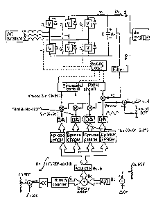
Fig. 10 is a bl~Nck diagram of a control system
for regulating the switching o~ the valves of a thxee phase
PWM converter, in accordance with ~he invention:
- ,~
:
-" ~L 3 ~
47
Fig. lla is a block diagram of a voltage
controlled oscillator circuit for frequenc:y control ~n a PWN
convert~r tation:
Fig. llb i8 a diagram of the frequency
with respect to the lnput voltage of the voltage
controlled oscillator shown in Fig. lla;
Fig. 12 is a diagram of a ~ounter circuit
Por use in voltage angle control;
Fig. 13a is a block diagram of an analog-
to-digital converter for use in direct voltage angle
control;
Fig. 13b is a table OI the binary output
of the analog-to-digital converter of Fig. 13a;
Fig. 13c is a diagram of a gating circuit
15 for controlling the analog-to-digital converter of
Fig. 13a;
Fig. 13d illustrates t~e wavefor~ pattern
of the gating circuit OI Fig. 13c;
Fig. 14 is a diagram of a binary adder ~or
20 voltage angle control in a PWM converter, in
accordance with the inv~ntion;
Fig. lS illustrates the synbol used
throughout the application to designate a PWM
converter module;
Fig. 16a is a diagram of a PWM converter
station with a plural ity of series connect~d PWM
converter modules;
Fig. 16b is a block diagram of a PWM
converter ~tation with a plurality of parallel
connected PWM conver~er modules;
Fig. 17 is a block diagram of a PWM
converter station comprising PWM converter modules
connect~d in series and in parallel;
~ ~3~
48
Fig. 18 is a blo~k diagram of the valves
control circuit of the converter statiQn ~hown in Fig~
17;
Fig. l9 is a diagram of wa~eform patterns
o~ carrier signals used to regulate the operation of
the valves of the converter station shown in Fig. 17;
Fig. ~0 is a diagram for a ~ilter
arrangement for us~ in a PWM converter;
Fig. 21 is a block diagram o~ a PWM
lo converter station illustrating schematically the
control system and its feedback loops for controllin~
the frequency, the voltage angle and the voltage
amplitude;
Fig. 22 is a diagram of a PWM converter
station connected to a DC and an AC network, the AC
network being representsd by its Theven~n equivalent;
Figs. 23a and 23b are phasor diagrams
showi~g the voltage angle control il a PWM conve~ter
in the rectifier and in the inverter mode
respectively;
Fig. 24 is a phasor diagram showing
lagging and unity power factor operation by changing
the voltage amplitude;
Fig. 25 is a diagram showing a negative
feedback implementation of a PWM converter operating
as a power dispatcher:
Fig. 26 is a diagram showing a negative
feedback implementation of a PWM converter operating
as a master DC voltage regulator;
Fig. 27a is a diagram of a PW~ converter
station with capacitor and inductor banks that can be
switched in quantized units by a logic control system;
,,
,
'~ ~
~ 3 ~ b .~
49
Fig. 27b is a diagram showing a V~R
waveform with respect to time in a PWM converter;
Fig. 28 is a typical schematic diagram of
a field excitation system of a synchronous ge~erator;
Fig. 29 is a diagram of a PW~ converter
with a supplementary control system ~or stability and
dynamic enhancement:
Fig. 30 is a diagram of a multi-terminal
HVDC connection;
FigO 31 is a diayram of a radial HVDC long
distance DC transmission line using PWM converters;
Fig. 32 is a diagram o~ a radial back-to-
back DC link using PWM converters; and
Fig. 33 is a diagram of a PW~ converter
station with complete controls.
To ~acilitate the understanding o~ th~
invention, the following description refers to some
basic principles. The description i~ organized under
the following sections:
Section Title
___ _. _
25 1 Valve;
2 Boost type P~M converter principles:
3 Implementation of the boost type PWM
converter
4 Multi-modules in series and parallel
connections;
Boost type PWM converter stations; and
6 Systems of boost type PWM converter
stations.
The starting point is the electronically
controlled power switch which is referred to as a
~ 3 2 ~f~
"valve" in this patent application. This valve can be
tur~ed ON and turned OFF b~ a logic ignal at the
gate. Section 1 defines exactly the meaning of the
term "valve" in this application and briefly describes
its principal characteristics.
Section 2 summarizes the principle of bi-
directional power transfer across a bridge converter
and also summarizes the pulse width modulation
principles. The intent of this section is to
emphasize that although there are many ways of
realizing the PWM principle, the end products are the
same, namely:
(a) the fundamental Fourier harmonic
component is enhanced while low harmonics are
suppressed and the residual harmonic components ar in
the high frequency end of the spectrum;
(b) the amplitude of the fundamental
Fourier harmonic component can be controlled directly:
(c) the frequency of the ~undamental
Fourier harmonic component can be controllad directly;
(d~ the phase angle of the fundamental
Fourier harmonic component can be controlled directly.
When the valves of the bridge converter
are turned ON and OFF in accordance to the PWM
principles, not only the end products can be realized
but the bi-directional power handling capability also
becomes a feature of the converter. The chief
attraction of this topology is that the DC link
voltage is unidirectional and bi-directional pow~r
transfer involves bi-directional DC link curren~ flow.
, ~ ' ' ' ',:
.'. . ' .''., '. ' ' ' ~'~ '
. .
~.3~32~
~1
Section 3 describes an exa~ple of a
control syst~ in a P~M converter, in whlch th~
fundamental Fourier harmonic component of tha ~oltage
at the 3-phase AC ter~nals of the PWM converter
responds to input signals controlling:
S1) the voltage amplitude;
(2) the voltage frequency: and
(3~ the voltage phase angle.
Section 4 is concerned with reaching v~ry
high voltages and very high current ratings expected
of a HYDC station. The example described in Section
4 is based on connecting a plurality o~ PWM converter
modules in series and in parallel. By staggering the
switching instants of the module~, the appearance of
~ast switching rates is achieved so that a very high
quaIity voltage waveform is realized. This is despite
of the fact that the valves in each module are
switching at a low rate. This has the advantage that
relatively slow valves can be u~ed. Another advantage
is that switching loss~s are reduced as the æwitching
rate of the individual valves is reduced.
Section 5 is concerned with a PWM
converter capable of handling megawatts and megavars.
The converter has 3 inputs: (1) AC voltage amplitude
control (2) AC voltage freguency control and (3)
AC voltage phase angle control.
By using the frequency control and the
phase angle control in a voltage lock 1QP, the PWN
converter can be synchronized and can remain
:,
,.,. : :
-~3~32.~
52
synchronized to the AC utility in spite of frequency
and voltag¢ angle dri~ts in the utilities.
The PWN converter can be configured into
one of the two basic building blocks:
(1) Power Dispatcher; and
(2) Ma~ter DC Voltage Requlator.
As a power dispatcher, the converter
maintains a constant delivery of the pow~r (recti~ier
or inverter power) assigned to it.
The master DC voltage regulatox maintains
the DC voltage assigned to it. It is basically a
power slack which assures that the algebraic sum of
the power into the DC system is equal to the oh~ic
losses in the DC transmission lins.
Each converter~ be it a power dispatcher
or ~aster DC voltage regulator, main~ains a regulated
voltage at the AC terminals thereof. I'he AC voltage
can be xaised or lowered by the amplitude control to
vary the reactive power intake.
Each converter is capable of handling
leading or lagging VARIs. For economic reasons,
switched capacitors and/or switch inductor~ may be
used. There is no need o~ static VAR controllers as
the continuous control of VAR's between the quantum
jumps between capacitor/inductor switchings can be
handled by the station itself.
.
:.
. : :
,:
2~
The three inputs: (1) amplitud~, (2~
frequency and (3) voltage pha~e angle are levers by
which supplementary controls for stability and dynamic
performance can be incorporated.
Section 6 considers two or several ~C
systems integrated throu~h a single DC network, based
on parallel connection of PWM converters. One ~tation
is the master DC voltage regulator in order to assure
the existence of the DC network voltage. The power
dispatchers fulfil their assignments with local
controls. As a power slack, the master DC voltage
regulator makes up ~or the power balance. The control
is extremely simple and does not need
telecommunication channels nor reversing switches.
1. ~AI~
The PWM converter, according to this
invention, is based on the electronically controlled,
electric power switch designated hereina~ter as
"valve" and which is represented by the black-box
symbol in Fig. 1.
The electric power switch terminals are
A and K. The path of unidirectional curr~nt ~low is
from terminal A to K. The valve has an ON-state and
an OFF-state.
The valve is turned ON by applying an
electronic signal to a terminal o~ the device. It can
also be turned OF~ by applying a signal to the sa~e or
another terminal speci~ically provided at this snd.
.
, . ~
.
.,' ~"
~3~32~
54
The valve shown in Fiq. 1, has only one gate terminal
G used to t~rn the valve ON and OFF, however, this
designation is intended to encompass a valve with
independent ON and OFF gate terminals.
When triggered ON, the resistancs between
A and K is low. When current passes from A to K, khe
voltage drop between A and K is low. When triggered
OFF, the resistance between A and K is high. E~en
when a very large positive voltage is applied from A
to K, the current which can flow from A to K is very
low. At all time~ when a reverse voltage is applied
(K having a positive polarity with respect to A), the
valve blocks, that is at most a very small leakage
current flows from K to A. Presently, based on
silicon technology, examples of such a valve are in
gate-turn o~f thyristor ~GTO), and gate-turn off
devices suoh as power bipolar transistors, power metal
oxide semiconductor ~ield e~fect transistor (MOSFET),
etc. The ~orce-commutated thyristor, where an
auxiliary thyristor in conjunction with a resonant LC
circuit, is also considered to come under the
definition of valve.
With the changing of technology, the
detail implementation of the ampli~ying circuitry
which steps up the trigger levels (micro watts) at the
gate to the power levels to effect a successful
transition from the OFF state to the ON state ~or vice
versa~, will also change. Likewise each device has
its individual characteristics requiring its speci~l
di/dt, dv/dt prot~ctions, snubbers, e~ergy recovery
circuits to reduce switching losses. The valve, as
.
: :'
-
, . , . ~
~3~
defined here, also covers the gate drive circu~ts andthe auxiliary circuits for di/dt, dv/dt protection,
snubbers, energy recovery circuits t~ reduce sw~tching
losses. It covers also the series diodes which may be
added to increase the reverse voltage blocking
capability.
The term valve also covers the logic
interlock circuits which prevent malfunction through
0 pOQr coordination. For example, in the single-phase
boost ty~e PWM converter of ~iy. 2, a "shoot through"
fault occurs when the upper valve and the lower valve
in the branch are simultaneously ON. The DC link
terminals are short-circuited, causing dangerously
large currents to ~low through the two simultaneously
ON valves. The inter-lock circuit ensures that both
valves in the same branch are never simultaneously ON.
One method of ensuring this is to introduce a time
delay between the turning OFF of one valve in the
branch before the other valve is turned ON.
Finally, the designation of valve covers
the series and/or the parallel connections o~ several,
closely matched, nearly identical electronically
controlled, electric power switches. Th~ series
connection is for the purpose of increasing the
voltage rating. The string of series connected
devices is between the terminals A and K of Fig. 1 and
they are turned ON and OFF in unison by electronic
trigger signal at the gate terminal G. There will be
auxiliary circuits to ensure that the voltage is
shared almost equally by each device, during steady-
state and transient conditions.
.
3~.32~i~
56
The parallel connection is for the purpose
of lncr asing the current rating. The devices
connected 1n parallel are 6ituated between A and K of
Fig. 1 and they are turned ON and OFF in unison by
electronic trigger signal at the gate terminal Go
There will be auxiliary circuits to ensure that the
current is shared almost equally by each device,
during steady-st~te and transient conditions.
In the practical world, the electronically
controlled, electric power switches can never be
turned ON or OFF simultaneously. By unison, ît is
meant here that the delays between the switches in the
transitions from ON to OFF state and vice versa, are
so minute as not to affect adversely the proper
functioning of the series and/or parall~l connection
of the switches, which are operated as a single unit,
namely the valve.
2 0 2 . BOO~T TYP~ ~N CO~Y~XR
The operation of the boost type PWM
co~verter is best explained in the context o~ the
single-phase case as shown in Fig. 2. In Fig. 2, the
valves VlU, V4L operate as one pair and V4U, YlL
operate together as the one pair. When one pair is
ON, the other pair OFF and vice versa.
2.1.1. Single Phase Bridge and Boost Prinoiple
The distinguishing features of the boost
type converters as illustrated in FigO 2 are:
(a) an inductance L is on the AC ~ide;
,. ~
. ~ :
.': . :
~3~32~
57
(b~ a capacitance C is o~ the DC link
side;
(c) th~ direction of current flow through
the four valves, (Vl~, VlL, V4U and V4~) is ~xom the
positive bus to th~ negative bus o~ ~he DC link: and
(d) the direction of current flow through
the four antiparallel diodes (DlU, DlL~ D4U and D4L)
is from the negative bus to the positive bus of the DC
link.
For the proper operation of the converter,
at all times, the DC link voltage Vc is higher than the
maximum amplitude of the voltage Va on the AC side.
The ensures that the anti-parallel diodes are normally
reverse-biased. The conduction of the diodes is only
possible with the help of the LdiJdt voltage of the
inductance L~ It is assumed here that the required Vc
is available through an external DC voltage source.
To understand the operation o~ the
converter, it is necessary only to discuss 4 cases:
Rectifier Operation i2>0 for ia>O and ia~O, and
Inverter Operation i2<0, for ia>0 and ia<0~
It should be noted that the four cases
cover axhaustively all concei~able operating
conditions. The DC link voltage Vc is unidirectional.
However, the AC voltage V~ can be sither positive or
negative, the only constraint being that the peak
value must be less than Vc. The AC attribute is
covered by the possibility that ia is treated or the
positive case and the negative case. In both
possibilities o~ ia~ it is show~ that a rectifier
~3~ 32~
58
operation i2>0 and an inverter operation i2<0 are
possible.
Rectifier Operation i2>o
For ia~o
Initially, VlL and V4U ar~ turned ON. The
voltage across the inductance ~ is Vc + Va and since it
is a positive voltage, the current ia increases, thus
building up storage magnetic ener~y in L~ As soon as
VlL and V4U are turned OFF, the current ia finds a path
through DlU and D4L. ~he diode conducts with the help
of the Ldia/dt voltage associated with th~ falling
current. The cycle repeats when VlL and V4U are
turned ON again.
In this brief cycle, there are two time
segments, ~t~ when the valves VlL and V4U are ON and
~t2 when they are OFF. In this cycle ia i1 change in
time as shown in Fig. 3~a). When ~tz~tl æo that the
time integral of the DC link current i1 is positive,
the converter is rectifying. The instantaneous DC
current i1 ~lows in the negative direction during ~t~
and in the positive direction during ~t2. The DC link
capacitor C acts as a bu~fer, as the voltage across it
25 i8 discharged during ~tl and charged during ~t2. The
load current i2 i5 unidirectional and positive when the
capacitor C is large enough to fîlter out th~
pulsations.
for ia<o
Initially, VlU and V4L are turned GN. The
voltage across the inductance is -(Vc - Va~. Since ia
is negative and the applied voltage is negative
~because Vc ~ Va), the negative current continues to
: . .
: ,
; ~,
.
~ .,
:,;
~3~
59
grow in the negative direction during the period ~t1
as shown in Fig. 3(b).
When VlU and V4~ are turned off, duriny
the time segment ~t2, the current ia finds a path
through the diodes D4U and DlL~ The diodes are made
~o conduct becaus~ of the Ldia/dt voltag~ is ~qual and
opposite to (Vc ~ Va). The current i1 on the DC link
side is shown in Fig. 3(b3. When the time interval dt2
is made greater than ~t1~ one sees that in the period
t2, the average DC link current is positive
showing that rectification is taking place. The
capacitor in the DC link acts as a filter and when the
perio~ ~t1 + ~t2 is small and the capacitor is large,
the output current iz is unidirectional and positive.
Inverter Operation i2~o
The average current in the DC link is
determined by the area enclosed by i1 in the time span
(~t1 + ~t2) and averaged over this time span. One sees
that by making ~tt ) ~t2, the nat current flow is
negative tfrom the DC link side to the AC side). This
corresponds to inverter operation.
~5 for ia)0
The ~witching o~ the valves is identical
to the rectifier operation, the current flowing
through VlL, V4U or DlU, D4L, except that ~t1 i5 longer
than ~t~. Fig. 4(a3 shows that ia and i1 have the same
pattern a~ in Fig. 3ta). From the area enclosed by i1~
it is easy to see that because ~t1)~t2, the average DC
link current is negative.
For ia~0
`
, ~:
~ ... ..
~ 3 ~
~o
The current path is through VlU, V4L or
DlL, D4U. ~rom Fig. 4(b), one sees how the average DC
link current i1 i8 nega~ive when the current $a is
negative. The switching o~ the valves is identical to
rectifier operation SQ that the currents patterns of
Fig. 4(b) are identical to Fig. 3(h) except for the
fact that ~t~ 2
2.l.2. Boost Principle and PWM
In Fig. 3 and 4, it is shown that the DC
link current i1 consists of a nagative current pulse in
~t1 and a positive pulse in ~t2 and the rectification
or inverter operation depends on their relati~e
durations in the ON-OFF time cycle At1~t2.
The PWM techniques consist of :applying
- successive ON=OFF cycles involving (At1+~t2~ of Fig. 3
and 4. The durations ~t1 and ~t2 in each cycle are
modulated so as to produce voltage or cuxrant
waveforms of certain specifications. While ~ulfilling
the specifiea objectives, the boost type topolo~y of
Fig. 2 enables a bidirectional power transfer.
2.2 Three Phase Bridge
The 3-phase bridge can be thought of as
three sets of the single phase ~ridge of Fig~ 2
connected together as shown in Fig. 5(a). The valves
and anti-diodes forming each phase are:
a-phase: lU, lL, 4U, 4L
b-phase: 2U, 2L, 5U~ 5L
c-phase: 3U, 3L, 6U, 6L
. ...
~'' ''`
13~3~
61
The current i~ in the neutral link i~
in ~ ia + ib + ic- Also from continuity of current
in + i~ + i~ = 0 where i~ and il are the currents of the
upper and the lower rails as defined in Fig. 5(a).
For operations under a condition when ia ~ ic - 0.
the neutral current in ~ and iu * i~ = 0~ Thi~
implies th~t the valves and anti-diodes 4U, 4L, 5U,
5L, 6U and 6L can be removed, lea~ing the 3-phase
bridge of Fig. 5(b~o
It should be noted that Fig. 5Sa) is
intended only ~or exemplary purposes. In fact, when
the three-phase bridge o~ Fig. 5(b) is made to operate
in the open neutral wye connection, a slight
complication arises because the neutral voltage ha~ 4
possible voltage levels
(0, + Vc / 3, ~ 2 Yc/ 3 and vc)
depending on the 23 = 8 possible swi~ching
states o~ the valves in the three branches. The
slight complication does not nullify the usefulness o~
Fig. 5(a) as an aid understanding the three-phase
bridge of Fig. 5(b~.
The points to stress here are that the
three-phase bridge o~ Fig. 5(b) is of the hoost type
with the following features: ~1) the inductance L i~
on the AC side of each phase, (2) the capacitor is on
the DC side, (3) the ~C link voltage is
unidirectional, the terminal d is positive with
respect to e, (4) the direction of current flow
through the valves are from the bus of te~minal d to
the bus of terminal e, (5) the direction o~ current
~low through the antiparallel diodes are from the bus
. ::
- .
:, ,: :
~3 ~ 3~
62
of terminal e to the bus of texminal d. As the AC
terminals a, b, and c are connected to a three phase
balanced wye connected AC supply and the valves are
triggered ON and OFF in accordance to one of the 3-
phase PWM strategies, the boost type topologyautomatically looks after the bi-directional powsr
~low by maintaining unidirectional voltaqe in th~ DC
link and bi-directional DC current flow. All the
other benefits of the PWM strategies are retained.
2~3 Pulse Width Modulation Principles
2.3.1. Single Phase Converter
Using the single-phase boost type
converter of Fig. 2 as an example, one sees that by
switching the valve pair (VlU, V4L) and its complement
valve pair ~VlL, V4U) ON and OFF repeatedly in a
cyclical pattern with the period 0 ( ~ ~ 2~, as shown
in Fig. 6(a3, the voltage Vkg between the terminals K
and H is of the form as shown in Fig. 6(~). In this
illustrative example, within the period 0 ( ~ ~ 2~,
there are ten switching instants at
Q1 ~ 2 ~ ~10
~he voltage Vkh(0) can be e~pressed as
Fourier Series.
r~ 3 = 0.5 CO~ ~ Cm sin (m~+~
m=l
where CO = 1 ~ V~ (8)d~
. . ., ~
~ 3 ~ 3 ~ ~L ~3
63
Cm = ~am2 ~ bm I
~m = flrc t~n I a~
r 2~
a = ~ ) cos?n~
1~ ~r J O
2Jr
b = 1 ~ (~)Si~n6
o
In general, the switching instants are not
limited to ten as used in the illustrative example.
For JMAX ~witching instants ~ jm~, there are
JMAX degrees of freedom for controlling the Fourier
coefficients, which are transcendental functions ~f
~1 ' ~2 ' - ~jma~ -
Cm = gm (~P ~ ~jma~)
Note that there are an infinite number o~
Fourier harmonic~ so that the JMAX (finite number)
degree of freedom are insufficient to suppress all the
ha~monics. At best, a number of low harmonic
components can have Cm=0. One degree of freedom must
be available to control the amplitude C1 o~ the
fundamental component. The remaining degrees of
.
.. ~ - . .....
, " ,
. . ~ , ~ ,
~3~3~
64
freedom may be used to reduce the overall harmonic
content. Fourier harmonics which are not suppressed
are tolerable in the high ~requency end of the
spectrum where the filters for them are r~latively
cheap to implement.
2.3.2 Sinusoidal PW~ (SPWM3
In sinusoidal PWM, the switching angles
~ 2,...Jm~are determined by th2 intersection points
of the carrier wave and the modulating wave as shown
in Fig. 7. The carrier wave consists of integra}
multiples of isosceles triangles fitted into the basic
period of the modulating wave. The modulating wave is
a sine wave of the fundamental period o ~ ~ ( 2~. The
amplitude of C1, the ~undamental Fourier harmonic
component of Fig. 6(b) varies dixectly with the
amplitude of~the modulating wave in Fig. 7.
20The implementation of SPWM may be analog
orientated or digital orientated.
Analog Orientated Implementation consists
of real time analog circuits which generate the
triangular carrier wave and the basic sinusoidal
modulating wavsform. The intersection points are
detected and are used to activate the gating logic
shown in Fig. 2 and 5. The amplitude control, V)n~,
of the modulating waveform is multiplied with the
basic sine-wave.
Digital Qrientated Implementation
j:';``~)
.,
:
:
/
~ 3 ~
6g
The triangular carrier wave and the basic
modulating sine wave are unifor~ly sampled in the
period 0 ( ~ ( 2~. The 6ampled poin~s are stored
digitally in two look-up tables. The look-up tables
are addressed by binary numbers n5, n3=0,1,2.. ,~Ns-1~
with the look-up tables containing the values o~ the
triangular wave, VT(ns2~/Ns), and the basic sine wave,
sin(ns2~/Ns). By using a counter ~modulo Ns) to scan
the addresses, and by comparing the output of the
triangular look-up table with the product o~ the
amplitude control with the basic sine wave, the
switching angles a1,~2,...~jm~ can be determined in real
time to activate the gating logic of Fig. 2 and Fig.
5.
Before concluding this section, it may be
added that there are minor variants to the method.
For example, the modulating wave may be a square or a
trapezoidal wave. The fundamental Fourier coefficient
C1 can be controlled linearly in a limited range by
varying the amplitude of the modulating wave.
2.3.3. Harmonic Elimination Principle
The harmonic elimination method is usually
implemented with a microcomputer with the help o~ a
look-up table containing the switching angles
~ 2~ jm~ corresponding to the desired amplitude of
the fundamental harmonic voltage C1. The contents of
the look-up ta~le have heen determined previously with
the help of a main-frame computer which solves
numerically for the angles ~ 2~ ajm~ required to
output the desired voltage C1 while sa~is~ying the
" !
' '.
',,
: . ' `''' "'.
, "
" ~ ', . ' ' "" ~ ' '
. . . ,',' . .
~ ~ ~ 3 ~
constr~int that the Fourier harmonic coefficients of
low harmonic order are zèro, that is
Cm ~ gm (~ 2~ m~) =Ofor some selected
values of m.
on solving the nonlinear transcendental
simultaneous equations, one has the switching angles
evaluated as functions of C1 that is:
~ 1 ~ C1 ) ~ ~2 ( C~ jm~r ( C1 )
which are stored in the look-up tablesr
Fron a command for a particular value of
C1, the angles are retrieved from the look-up table and
the pulse widths are generated in real time with the
help of down counters.
2.3.4. Three Phase Converter
In the single phase converter of Fig. 2,
the PWM control consists o~ sending gate logic signal
to valve VlU as illustrated by Fig. 6(a). The logic
signal to Vl~ is the complement to the logic s~gnal
sent to VlU. The switching angles al,~2. aJm~ are
determined by the SPWM strategy discussed i~ Section
2.3.2. or the harmonic elimination strategy discussed
in section 2.3.3.
In the three-phase implementation o the
converter of Fig. 5Ib~, the gate logic siynals to
drive the valves V2U and V2L of the B-phase and the
valves V3U and V3L of the C-phase are each generated
in the same way as th~ A-phase except *or an angle
delay of -2~/3 and -4~/3 for the B- and C-phase
. ,
: .
~3~3~
67
respectively. De cribing the logic state of Vl~ of
Fig. 6(a) a~ VlU(~), then the logic ~ate o~ the valve
V2U of the B-phase is V2U(~=VlU(~-2~/3) and the logic
state of Y3U of the C-phase is V3U(~)-VlU(~-4~/3).
2.4 Voltage Amplitude Control
Using any one of the PWM principle~
described in Section 2.3, there is a controllable
range in which the fundamental harmonic component of
voltagc C1 is linearly dependent o an input signal
Vmodc
As the low order harmonics are suppressed
by the PWM techniques and the high harmonics can be
removed by economical filters, only the fundamental
hanmonic component of voltage will continue to be the
subject in the discussion.
.
The point to emphasize is that the pha~e-
to-neutral voltages of three phases are: C1sin (~
Ctsin ~ 2~/3) and C1sin (~ 4~/3) where Cl is
proportional to an amplitude control signal Vm~c.
2.5 Frequency Control
Irrespec~ive of whether the method is by
SPWM or by harmonic elimination principle, the PWM
strategies are based on locating the switching angles
30 ~ 2.~ m~ in the basic period 0 ~ ~ ( 2~. This
period can be cycled through at a fast or slow rate
without affecting the linear relationship of Cl wi~h
~`.' :' - .:
~3~3~
6~
the amplitude control Vm~c. Thu~ amplitude control
and ~reguency control are independent o~ each other.
By de~inition, the angle 0 is related to
the angular frequency control by the ~ollowing
relationship.
d~ = w
d~
~ I t
For constant frequency control, the A-
phase voltage is C1sin~ct~
A convenient implementation o~ thefrequency controller is through the use of the ~CO
tVoltage Controller Oscillator). In one form of the
VCO, the output is a square waYe whose frPquency is
proportional to the voltage applied to its ~nput.
Thus the frequency command ~c is inputted as a voltage
to the VCO and the count of the square wave outpu~
used as a measure of ~.
2.~ Voltage Angle Control
As a major aspect of this inYentiOn iS the
voltage angle control, this section is devoted to
clarifying i~s exact meaning. Considering one phase
o~ the PWM boost type converter represented as an
. ~ .;,, ,,, ,,.,~.,.".,,,.. .; .. -. ...
~L3~3~
6~
ideal voltage source in Fig. 8, the fundamental
harmonic voltage is expressed mathematically as
C~sin(~ct-~c). Let us consider the corresponding phase
of the utility power supply to which it will be
synchronized. The equivalent Thevenin voltage is
V ~sin(~St-~5) as shown in Figure 8. Ths power 8upply
frequency ~s dri~ts slightly over a long time period
but for our discussion, it is assumed constant. For
synchronization to be possible the converter frPquency
~C ~ust be made equal to the utility frequency ~.
The voltage angle in question is de~ined
as (~0c) where ~C=~ct-~ and ~S=~St-~S. The voltage
angle control can be direct or indirect.
Fig. 9 displays the ~-vs-time and the ~-
vs~time curves to emphasize that the voltage angle is
the time integral of the angular ~requency. As such
it is possible to control the voltage angle indirectly
by jogging the frequency control forward or backward.
Direct voltage angle control by-paæses the
frequency control altogether. This i~ illustrated in
Fig. g(a).
2.6.1 Indirect Voltage Angle Control
by Integrating Frequency
~ig. 9(b) shows the case where initially
3 ~ ~s=~c ~5=~ In order to advance the voltage angle o~
~c~c is increased momentarily. The voltage angle
.. . ~ .
~ . .
,:
3L3~2^~
advance is kept constant when ~c=~s~ The angle can be
retarded by decreasing ~c
The input voltage V~ to the VCO controls
its counting rate and effectivsly the time ba~e.
3. IMPLEMENTATTON OF BOOST TYPE PWM COMY~RTER
Figure 10 shows in a block-diagram form,
the implementation of the controls of the basi~ boost
type converter bridge module of Fig. 5(b).
The sinusoida} PWM (SPWM) principle is
used in this implementation. This consists of
generating a triangular carrier and three basi~ sine-
wave modulating signals for each of the three phases.
The switching angles are based on the intersection o~
the carrier wave~orm and the mod~llating wavefor~s.
The block labelled "sinusoidal P~M control circuit"
accepts as inputs the modulating ~ignals of each of
the three phases and the triangular carrier signal and
outputs the ~iming signals to the yating logic of the
valves. The implementation of this function is well
known and will not ~e discussed further.
The key issues consists of the
implementation of the three control ~unctions so that
the phase to neutral voltages of terminals a, b and c
have fundamental harmonic components of the ~orm:
C1sin(~+~l), C1~in(~+~1-120) and C1sin(~+~l-2400).
i,. .
13~3~
The thxee control ~unctlon~ are:
(l) Vm~c which control~ the voltage
amplitude Cl;
(2) ~cwhich controls the voltage angular
frequency ~; and
(3) ~c which controls ~he voltage phase
angle 'P1'
As shown in Fig. 10, each of these control
functions is in the form of an analog signal, obtained
over an adjustable ranye using a potentiometer as a
voltage divider. The reference settings for the
voltage amplitude, frequency and voltage angle are
resp~ctively nREF~ ~m~F and ~REF. Electronic adders
are provided so that feedback ~ignals of the voltage
amplitude avm~C frequency ~ and voltage angle ~c can
be included so that
Vmodc--VmodREF~Vmodc
~c-QREF~Q~c .
0C = ~ dc
As shown in Fig. 10, the input ~c which is
an analog voltage, controls the frequency of the
pulsed output of the voltage controlled o~cillator
~VCO). The VCO output pulses are counted by a binary
counter. The counting of the ~ulses corresponds to
the time integration of the frequency of ~cr The
contents of the binary counter is therefore a mea~ure
(in binary digits) of the voltage angle ~O When the
. -
- , :
, . ~ .-...... .
. .......... :.
"'' ' ;' .; 'i ,,
~ 3 ~ q~
72
pulse rate is high, the voltage angle ~ in~reases at
a high rat~ (the rate being the frequency~. It should
be noted that the binary counter has a ~inite numb~r
of bits and when the count reaches 111..~111, the next
count resets it to 000... 000~
The cyclical property fits exactly the
voltage angle measure desire~ of the system. This is
because in the harmonic functions, the basic
repetition period is O ( ~ ~ 2~ and in the binary
counter the repetition period is 000...000 to
111...111. ~ach binary number in the counter is a
discretized representation of the angle ~. Since the
angle is kept increasing by the VCO, it is indirectly
controlled by the frequency input, ~c
Using a digital adder, one can add one
binary number to another binary number in real time.
This enables d~ect vo~tage ongk ~ontrol to be implemented.
As shown in Fig. 10, the direct angle control ~c=~c
is originally an analog signal. It is converted by an
A/D (analog-to-digital~ converter to a binary digital
number.
Using a binary adder, the binary number
representing ~c is added to the contents of the binary
counter. As the VCO keeps pulsing, the binary counter
keeps increasing. The voltage angle ~ which is
introduced by the binaxy adder is the angle shift with
respect to the angle represented by the content in the
binary counter.
~ 3~3~
73
As shown in Fig. 10, the output o~ the
binary adder i6 used as the binary address of ~our
look-up tables which ara implemented by ~PROM's. As
the look-up tables are addressed, their contents in
the address which ar~ in binary ~orm, are converted by
D/A (digital-to-analog) conv rters with sample and
hold features.
The contentæ of the look-up tables depend
on the PWM strategy which is employed. In the
sinusoidal PWM ~trategy which has been adopted, as the
YCO continues to pulse, the analog outputs of the D/A
of the A-phase EPROM, the B-phase EPROM and C-phase
EPROM are the discretized form o~ sin~, sin(~'l20)
and sin(6~240~). The output of the carrier EPROM
consists of the discretized for~ of the triangular
carrierO
Voltage amplitude control is accomplished
by electronically multiplying the three basic sine~
waves outputs by the D/A of the EPROMs by the control
signal Vm~C=Vm~EF~Vm~c -
The trianqular carrier signal is
electronically multiplied by a signal which isproportional to the DC link voltage Vc. This ensures
that the amplitude of the AC voltage i~ independent of
variations in Vc.
Within the block labelled "sinusoidal PWM
control circuit", the information from the A-phase
modulating signal and the triangular carrier signal
are used to generate the g~ting logic signals to
: ``''~`:
^~ .
~ . . . .
,
- .
: ' ,
~3~ 32~
74
swltch the valves sf the A-phase in the three-phase
bridge~ The switching angles ar~ based on the
intersection~ o~ ~he modul~ting waveform and the
rarrier waveform.
The same principle is used for the B-phase
and the C-phase.
3.1 Freguency Control
Fig. ll(a) shows the control circuitry to
a voltage controlled oscillator VC0. As shown in Fig.
ll(b) the frequency o~ the pulse output of the VC0 is
linearly proportional to the input voltage. In this
embodiment for a utility frequency of 60 Hæ, an output
frequency of n~EF+60x2l2=245,760 Hz has been selected.
This frequency is obtained at an input voltage
VinvcO=~VDD specified by the ~anufacturer of the
VCOSC~404~) .
The input voltage is obtained from a
potentiometer where the voltage of the frequ~ncy
setting Q~EF can be adjusted. The operational
amplifier LM 747 of Fig. ll(a) serves as part of an
adder so that the voltage corresponding to the
feedback signal ~c can be added so that the frequency
reguest of the VC0 is ~c= (nR~F+~C) -
3.2 Frequency Track by Feedback
Note that because of drifts in the voltageof the power supplies, in the amplifier gains and in
the circuit components, the desired fre~uency nREF
13~32~
does not remain con~tant. In actual fact ~REF should
be in synchronism with the frequency of the utility
~ystem to which the converter is to b~ connected. The
frequency of the utility system does drift to a
certain extent and the voltage ansle changes with the
power loading. The terminal ~c allows a negative
f~edback loop to be ~ormed to ensure that the
converter frequency is always synchronized with the
utility system in spite of the drifts.
As will be seen in section 5.4 and 5.5,
the frequency feedback is strengthened by the voltage
angle lock loop.
3.3.1 Voltage Angle Indirectly Controlled by a VCO
Fig. 12 shows three 4;bit binary counter~
which are incremented by th~ pulsed output of the VCO.
When the VCO frequency is n~EF=245,760 Hz, the
frequency o~ the highest ~it is fC1t-60 Hz. The 9 high
bits of the counter (C3-CIl) are used to control the
EPROM addresses. As 29-Sl2, this means that the basic
period 0 ~ ~ ( 2~ in Fig. 6 is discr~tized into 512
intervals and each interval is identified by a binary
number. As the VCO keeps pulsing and the counter
keeps increasing ~modulo-512), the angle axis is being
scanned repeatedly Prom ~=0 to &2~. The pulsing rate
of the VCO determines the frequency of the scan.
3.3.2 Direct Voltage Angle Control
Using a Digital Adder
, - ~
.
;'
` - -
~ 3 ~
76
As sho~n in Fig. ~O, the analogue signal
~, which shifts the voltage angle directly, consists
of a reference settin~ ~cREF which is obtained through
a voltage divider and a ~eedback signal ~c The two
analog signals are added by electronic adders.
The details of impl~menting the direct
voltage angle control are described in Figs, 13 and
14. There are two parts: (1) A/D con~ersion oP
and (2) binary digit addition~
3.3.3 A/D Conver~ion of ~c
As shown in Fig. 13(a), the input of 0c is
converted by an A/D converter (A~C 0804) into a 9 bit
binary nu~ber (D8-D0).
Fig. 13~b) shows the conversion of the
analog values Of ~c from 0 to 2.5 V into digital f~rm.
The analog voltage 2.5 V represents ~c=~ V
represents _9OD and 5V represents ~90. The
discretion level is 5 V/25S=0.0195 mV per bit. Each
bit increment represents 0.703.
Fig. 13 (c) shows the output lines o~ the
counter C2, C3, C4 and C5 being co~bined in logic
circuits to control the latch, the WR and the RD
terminals o~ the A/D converter~
~ ~ '
~ 3 ~
Fig. 13(d) show~ the timing diagram.
3.3.4 Binaxy Addition
The control signal ~c expressed in the
digital form in 20 lines D8~DO are added to the
contents of the binary counter Cll-C3 using the binary
adder shown ln Fig. 14. The sum which is expr~ssed as
a binary n~mber in the output lines A8~AO is used as
}o the address of the EPROM's.
Returning the voltage angle axis o~ Figs.
6 and 7, the address in (A8-AO) corresponds to the
angle
~ t
~ ~ J [nREF(r) ~ (r)]dT + ~c
where the time integral is contained in the counter in
[Cll-C3), while the direct angle control ~c is
contained in (D8-DO).
~5
3.4 Digitized Waveforms in EPROM
The method of implementing the: SPW~
control has consisted of disrretizing the period C ~
~ ( 2~ o~ Fig. 7 into Ns (512) sample points, so that
the number~ nS=0,1,2...(Ns-l) corresponds to th~
interval 2~nJNs( ~ ( 2~ (ns+l~Ns. The numbers
ns=0,1,2...(Ns-1~ expressed in the binary ~orm are used
as address~s of four look up tables. The addressing
f nS is from the lines A8-AO from the adder of Fig~
, ' ' ~ ', ' ~ ' ,
.
.
~3 ~ 3~
~8
14. As the counter (Cll~C3~ keeps on increasing, the
look-up tables are repeatedly scanned (with modulo ~5~
The look-up tables of the A, B and C
phases contain in its * address the information o~ the
basic sinusoidal waveforms sin(2~ns~Ns), sin~ (2~ns/Ns)-
2~/3] and ~in[(2~nJNs)-4~/3]. The fourth look-up
table contains the information of the triangular
carrier waveform.
The look-up tables are implemented by
EPROM's with the contents stored as bits.
As shown in Fi~. 10, the four EPROM'~ are
simultaneously addressed by the address reglster
(A8-AO) and the binary information in the EPROM's are
converted by D/A ~digital-to-analog converters) to
analog voltages which reconstruct the sinusoidal
modulating waveforms and the triangular carrier
waveform.
3.5 Voltage Amplitude Control
Using the Sinusoidal PWM strategy, the
amplitude of the fundamental harmonic component has
the formula:
Vm~cVc
Vr
where
~3~3~
79
Vm~c- peak value of sinuæoidal modul~ting
wave~orm
~ = peaX value of triangular carrier
Vc = DC link voltage
The voltag~ amplitude control i~ ba~ed on
implem~nting the above formula.
As shown in Fig. 10 the voltage amplitude
control Vm~C consists of two parts: (1) a voltagie
amplitude reference Vm~RE~ setting obtained fro~ a
voltage divider, (2) a feedback voltage ~Vm~c. The
two analog signals are added electronically so that
Vmodc=VmodREF~ QVmodc
The yoltage amplitude control signal is
electronically multiplied to earh of the basic
sinusoidal waveform signals emerging from the D/A
converters of the EPROM's of the A, B and C phases.
In order to ensure that Cl is not affected
by the change~ in the DC link voltage Vc, the output
waveform o~ the txiangular carriex EPROM is multiplied
by a signal which is proportional to Vc. This signal
is obtained from a voltage transducer acros~ the DC
link and is passed through a filter which removes the
residual switching ripples. Since the peak value of
the triangular carrier V~ is made proportional to Vc,
the voltage amplitude C1 i5 independent of Vc.
`'' '
: .:
::: . .... .
~ 3 ~
8~
4~ MULTI MO~ULES IN SERIES ~ND IN PARALLEL
TO INrREASE THE VOLTAGE AND THE CURRENT R~TINGS
In Section 1, it has baen stated that the
valve which i~ represented by the symbol of Fig. 1 ~ay
in fact consist of a number of series and/or parall 1
connectsd electronically controlled power switch
devices (GTOs,MCTs, power bipolar transistors, power
MOSFETS, etc.~ for the purpose of increasing the
voltage withstand limit and th~ current carryinq of
the ~alve. Some elactronically controlled power
switch devices are not easy to connect in serie~
and/or in parallel. The voltage and current stre6ses
may not be easily distributed evenly among the
devices. The devices may not switch ON and OFF
simultaneously.
- In the even~ that the ~eries and/or
parallel connections cannot be easily accomplished at
the device level within the individual valve, the
voltage rating and the current rating can be increased
by connecting converter modules in series and in
parallel.
4.1 Boost Type PWM Converter Module
Fig. 15 is the symbol of the PWM Boost
Type Con~erter Module of Fig. 5(b).
,,
' - ,
-.
~3~ 3~ ~
81
4.2 Serie~ Connection
Fig. 16(a) shows Nr modular u~its
connected in series. The AC supply terminals have to
"float" so that the DC link voltages can be added as
~ DCT = ~ v~
The voltage sharing across each module is
determined by the tolerance of the circuit parameters
Ih, Cn and the AC ~upply voltage. The valves in the
same phase do not have to switch simultaneou~ly.
4.3 Parallel Connections
Fig. 16(b) shows Nc modular PWM converter
units connected in parallel for the purpose of
increasing the current carrying capability in both ~he
AC side and the DC side. The DC output voltage is
common to all the modules. The inductances ~1,
L2...~ cenable the modules to be connected to a
common three-phase AC bus. When khe inductances Ll,
L2...~C are manufactured to close tolerances, the
current is shared evenly by the modules. The valves
of the same phase do not have to be switched ON and
OFF in unison for parallel connection to succeed.
4.~ Boo~ Type PWM HVDC Station
In order to attain the high voltage and
the high current rating required of a HVDC
.. :
. . ~ , ,.
': .:
, :`;. ,; ~, . .
~3~ 3~
~2
application, a matrix of N~xNc modules arranged in
series and ln parallel as shown in Fig. 17 is used.
4.4.1 Filters
on the AC side, the terminals o~ the
station are A, B and C. A ~ilter at each phase
removes the high frequency harmonics so that none
enters the utility system. There are ~everal possible
versions of the transformer connections.
4.4.2 Transformers
In the example shown in Fig. 17, there i8
a separate transformer for each phase. In each of the
identically built transformers there is a single
primary winding. For each transformer, there are Nv
secondaries, each with the same number of turnæ.
The insulation between the secondary
windings should be adequate to withstand the
difference in DG voltage between them. This i8
because each of the secondary winding is connected to
Nc converter modules in parallel and is associated with
a DC voltage Vc~v across the commo~ capacitor across
the DC link terminals. As the DC link capacitors are
connected in series so that the total volta~e across
the terminals D and E consist o~ V~1+Vc2~ --Vcn~ it is
required that (i) the secondary windings of the
terminals should float and that (ii) the insulation of
the secondary windings should be sufficient to
withstand the difference in DC voltages between them~
- `
~ 3 ~
4.4.3 Floating Neutral
As shown in Fig. 17, the undotted
terminals of the i=l secondary of the A, B and C phase
are connPcted in wye. The neutral is left to ~'~lcat~9.
Although not shown, the undotted terminals
o~ the i-l secondary o~ the A, B and C phase should be
connected in wye and th~ neu~ral terminal is left to
"float". This connection is applied to all the
secondary windings i=1,2,...NV.
~ he l7floating" secondaries enable the DC
outputs of the converter modules belonging to the same
row to be added so as to increase the total DC output
voltage across terminals D and E.
4.4.4 ith Secondary AC Bus
The dotted terminals of the ith
transformer secondary of the Am, B and C phases are
the terminals connecting the 3-phase AC bus system oE
the ith row of the converter modules. From the ith AC
bus, the connections are made to the Nc parallel
converter modules at the terminals a, b/ c.
4.4.5 ith DC Bus
The d, e terminals of each o~ the Nc
parallel converter modules o~ the ith row are all
connected in parallel to the DC bus. The D bus has
a common capacitor Cjacross it and the DC voltage
across it is Vci.
:'
:.. .: ::.. . .
: ~ ,
.:~ . ..
-
~ 3 ~ $
84
4.4.6 Plug-In for service and ~aintenance
As each onvertar module in the matrix of
Fig. 17 is connected to the AC-bus to the t rminals a,
b, c and to the DC bus to the terminals d,e it can be
disconnected easily ~or service and maintenanceO
As there is always a danger involved in
"live" maintenance, a defective module can be le~t in
the circuit until the regular maintenance period. The
valves should be turned off and the local cixcuit
breakers activated to disconnect the module from the
AC bus at the points a, b, c and from the DC bus at
the points d, e.
4.5 Multi-Module Control
Based on the block di~grams of the control
circuitry outlined in Fig. 10, the control of the
matrix of NvxNc converter modules of Fig. 17 is shown
in Fig. 18. Each block labelled SPWM in Fig. 18 is
the ~inusoidal PWM control circuit block of Fig. 10~
The sinusoidal PWM control circuit accepts an analog
signal of the triangular carrier waveform and an
analog signal o~ the modulating sine waveform of the
A-phase, of the B-phase and of the C-phase. Th~re are
altogether four analog signal linas. The SPWM control
circuit block detects the points of intersection of
the modulating wave~orm with the triangular carrier
waveform (as shown in Fig. 7~ and sends tha g~ting
logic signals to the upper and the lower valve o~ the
corresponding phase so as to swit~h them ON or O~F
. . .
., ., , .-.,
11 3 ~
thus generating the pulse width modulated voltages o~
Fig. 6(a)-
As shown in Fig. 18, each of the ijth unit
(i=1,2...N~=1,2...NC) receives the same ~odulatingwavefor~ for the A, B and C phase. The analog sign~ls
of the modulating waveforms are converted by the D/A's
~rom the look-up tablets stored in the three EPROMs.
The EPROMs are scanned by the ADDRESS. The VCO and
10 CQUNTER in Fig. 10 implement the function of fre~uency
control. The A/D and ADDER i~plements the function o~
direct angle control. The amplitude control is
achieved by electronically multiplying Vmodc to the
analog output lines.
4 . 6 Harmonic Elimination by Shifted Carrier
- As shown in Fig. 18, each module has a
separate EPROM for its triangular carrier wavefQrm.
20 E:ach carrier waveform EPROM i~ addressed by the same
ADDRESS. Essentially, each EPROM contains the same
information to generate the triangular carrier
waveform as illustrated în Fig. 7~ The only
difference is that the triangular carrier waveform of
25 each module has its allotted phase shift which is an
integral multiple o~ ~sh.
As illustrated in Fig. 19, there are N~,l
triangles in the period 0 ( ~ ~ 2~ 80 that the period
30 of each triangle is 2~rNtn, The basic carrier angle
shi~t for (NcxNv) modules is
.
.
~ 3 ~ . 9
86
~, 2rr x
Nb,~ ~Nc x Nv)
The solid line and the dashed l~ne
illustrate the principle of the shifted carri~r. ~hen
the triangular carrier wave~orm of Fig. 19 is
described mathematically as: Tr(~), then the shi~ted
carrier of the ijth module of Fig. 18 is
Trij(~ )Nv+j]esh)
when the contents of each EPROM contain the digitized
form of Trij~), for i=1,2...NV and j=1,2,...~C, it can
be proved mathe~atically that all harmonics are
eliminated until the (NtnxNcxNv3 th harmonic. This
harmonic elimination principle has been demon~trated
by experiment and by digital simulation.
The reason for using the principle o~
phase angle shifted carrier is that for the same high
quality of output voltage waveform on the primaxy side
of th~ transformers in Fig. 17, the valYes in earh o~
the converter modules do not have to switch at a fast
rate. Having chosen a value for the (NtnxNcxNv~ as the
lowest uneliminated harmonic number, the number o~
triangles Ntn in each cycle does not hav~ to be a big
number when the number of modules employed i~ the
station (Nc x Nc) is large. This i~plies that
relatively slow electronically trigyered pow~r
~witches such as GTOs or e~en force-commutated
thyristor~ can be used as valves. This has the
'` ' ~
-- 3~L32~
87
further implication that the switching losses are
reduced by l/(NcX~r)
The phase angle shi~t principle
S essentialiy staggers the switching instants of NcxNv
modules so as to give the appearance of a fast
switching rateO
4.7 Even Distribution o~ Voltage Stress
Althou~h the voltage across D and ~ in
Fig. 17 has to be a high voltage for HVDC
transmission, the voltage stress across each valve in
each module is only 1/Nv. By care~ul design of the
tra~sformers, the inductors L and the capacitors C,
the voltage vc; across the DC link capacitor Ci can be
made approximately equal.
4.8 Even distribution of Current Stress
By Making the transformer voltages, the
inductances L and the capacitances C to be equal
within reasonable tolerances, the current through the
valves are evenly distributed. Thus the current
carrying capability is increased by N~ times that of a
single module.
4.9 Transformers
In Fig. 17, the transformer of each phase
consists of a s;ngle primary winding with NY separa~e
secondary windings. The secondary windings are made
.
, . ~
.
-.. ~.,~
~: . . . .
`": ' ` :
. ~, .
:
.. ~ .
~ 3~ 32 ~
from identical coils so as to yield identical
voltages. The insulation coordination o~ the
secondary windings must take into account the
difference of the DC voltage between the secondary
coils.
An alternative scheme is to have for eac~
phase N~ separate transformers, each having one
prim~ry winding and one or more separate secondaries.
The total number of separate secondaries is Nv. The
secondary windings produce identical voltages. The Nvp
primaries may be connected in series and/or in
parallel depending on the requirements which must be
satisfied.
In all case~, the floating secondaries of
the 3-phases are arranged in the floating wy
connection of Fig. 17.
4.10 Harmonic Filters
Harmonic filter design is a well known ar~
in HVDC. Typically, the ~ilter consists of arrays of
series Lk, Ck elements tuned o that the resonant
freguency
Wk = 1~ \~
coincides with one of the harmonic frequencies which
are emitted. In addition, a high pass filter is
included to remove the remaining harmonics not
suppressed by the tuned circuits.
,
.
.. .. ..
~ 3~3~1~
Fig. 20 shows a typical filter
arrangement. In SPWM application, the harmonics wh;.ch
are to be removed are in the high frequency range so
that the Lk, Ckelements are relatively small an~ cheap.
5. B005T TYPE PWM HVDC STATION
5.1 Boost Type PWM HVDC Station
The boost type PWM HVDC s~ation is
represented by the diagram of Fig. 21.
The AC power terminals A, B, C in Fig. 21
correspond to the terminals A,B.C in Fig. 17.
Likewise, the DC power terminals D and E, in Flg. 2~,
are the same as in Fig. 17. Between the AC power
terminals and the DC power terminals of Fig. 21 are
the harmonic filter~, the-three phase trans~ormers,
the inductors L and the capacitors ~, the matrix of
three phase PW~ bridge modules connected in series
and/or in parallel as shown in Fig. 17. Each module
has the circuit shown in Fig. 5(b). The modules are
operated in the SPWM strategy using the control scheme
of Fig. 18 and Fig. lOo As shown in Fig. 10, there
are 3 controls:
Sa~ Voltage amplitude control (Vmodnc);
(b) Frequency control ~nc): and
(c) Direct Voltage Angle Control (9nc)0
Frequency and direct angle controI are not
independent and to emphasize that the voltage angle is
' '' ~` ` '
::,
'" ''
321~
a time integral of frequency, the diagram of Fig. 21
includes the integration block.
The box M in Fig. 21 represents ~he
measurements which can be made available for feedback
control purpoæes. The quantities which are routinely
measured are: AC voltage amplitude, AC current,
three-pha~e AC real power, three-phase reactive power,
phase angl~, frequency, DC link volta~e, DC link
lo curr~nt, DC link power, etc. It is within the present
art to make these measurements and no further
ela~oration is necessary.
In this section, the boost type HVDC
station of Fig. 21 is viewed in terms of terminal
characteristics. When the DC link terminals D,~ has
a voltage YCn which is large enough to ensure that all
the ~ntiparallel diodes are normally reversed bias~d
and when the valves are switching regularly under the
2~ SPWM principle, then the line-to-neutral voltages cf
th~ terminals A, B, C have a fundamental Fourier
harmonic component of the form
Van = \~ VmodnSin (Wnt + ~n)
Vbn \~ VmOd"sin (Wnt ~ t1n ~ 120 )
Vcn \~ VmOdnsin ~Wnt ~ /~n 240 )
The diagram of Fig. 21 highlights the fact
that the Voltage amplitude, ~requency and an~le are
controlla~le by VmOdnc~ Wnc and ~nc- It is by making use
o~ these controls in feedback loops that th~ same ~VDC
,- ~
.~....
~3~
91
~ta~ion can be made to perform different functions and
in i~tegrating several AC Bystem into a co~mon DC
network.
When the AC ter~inals are connec~ed to an
AC system, fundamen~al Fourier current cvmponent are:
ian \~ InSin (Wn~ + ~n ~ ~Xn~
ibn = \~ InSin (Wn~ ~ ~n t an ~ 120)
~ nSln (Wnt + 9n + ~n ~ 240)
where ~n is the phase angle.
Neglecting switchin~ losses, the power
balance equation allows the DC link output current i2n
to be calculated:
i2~ + Vonian +Vbnibn - Vcn~n
2 5 vcn
The boost type HVDC station admits currenk
at any power angla, Oc~nc360. Furthermore, power
reversal is achieved by negative direction in the flow
o~ the DC link current, when cs~n is a negative
number, i.e. 900<~c270O.
5.2 Boost Type PWM HVDC Station-vs-Generator Station
The direct control over the 3-phas~
voltages on:
,,
. .
.: -
~3~32~
92
~1) amplitude,
(2) frequency and
(3) voltage a~gle,
makes the boost type PWM ~VDC functionally equlv~lent
to the generator station.
In the generator station, the voltage
amplitu~e is controlled through the field excitation
system by voltage requlation. Voltage amplitude
serves two ~unctions. (i~ r~active voltage control
(ii) supplementary control for impro~ing stability and
dynamic respons~.
In the generator station, the governor
system regulates the frequen¢y and the real power
delivered through the power angle. The governor
system opens or closes the valves o~ th~ steam or
hydro-penstocks in response to the demand.
As the boost type PW~ HVDC station has the
sa~e three-levels of control, the capabilities o~ the
generator station are duplicated easily. Because the
PWM HVDC station has a fasker response than the
generator station, many of the functions can even be
done better.
5.3 Utility System Environment
Fig. 22 shows on a sinql~ line diagram the
nth boost type PWM XVDC station of Fig~ 21 connected
to an AC system. The AC system is representsd by the
Thevenin voltage Vn and the Thevenin impedance Rn~jXn.
As Rn is usually very small compared to Xn, it is
.
.. '.. ~ .
,
~3~3~
~3
neglected hereafter. It is assumed that the DC side
has a sustained DC voltage Vcn.
There are several poi~ts which must be
noted concerning the AC system. Firstly, the
freguency of the entire system drift~ gradually over
a ].ong period around the nnminal 50 Hz or 60 Hz. The
magnitude of ~he frequency drift may ~e quite small
but all the same, the PWM HVDC station, which
generates its own AC voltage, must track the frequency
drift.
The second point to note is ~hat the
topology of the AC system is continually changing as
dif~erent generator units are switched ON or OFF the
lines in pursuance o~ some unit co~mitment s~hedules.
The loads are themselves being connected or removed
from line. As a result, the Thevenin impedance Rn+jXn
varies with time.
Furthermore, because the different
stations in the power pool have different load ~low
schedules, the amplitude of Vn and ~ts voltage angle
also change in time~
In order for the boost type PWM HVDC
station to operate in such a dynamic environmen~
must have a voltage angle lock loop which ensures that
the AC system and the DC system will hang together.
In addition to hanging together, the HVDC
station must be capable of fulfilling some assigned
function. As will be described) the following
-
~3~3~
94
~unctions can be imparted in the PW~ HVDC stations ~y
designing the feedback loops:
(1) Power dispatcher; and
(2) Master DC voltage regulator ~power
slack).
5.3.1 Real Power Control by Voltage Angle
Real power is controlled through the
voltage angle. This is illustrated through the phasor
diagram of Fiy. 23, where the voltage amplit~de of the
PWM HVDC station ¦Vmodc¦ is made equal to the
amplitude o~ the Thevenin voltage ¦ V~ ¦ . Assuming
Rn=O, the voltage drip jXnIn is the closing side o~
the voltage trianqle subtended by the angle ~n. The
current ln makes an angle ~2 between the two voltage
phasors. In fact, it can be easily proven that the
pow r converted from AC to DC is
P=-3[¦Vm~nI¦V"Isin~n/Xn], so that power i~ controlled
through the voltage angle ~. Fig. 23(a) and ~b) æhow
that for negative and positive values ~ ~n the PWM
HVDC station is operating as a rectifier and an
inverter respectively.
Note that ~nC= corresponds to the voltage
angle o~ the Thevenin voltage. This is the voltage
angle at the t~r~inals of the utility system, just
before the synchronizing switches are closed for
connecting the PWM HVDC station to the AC system. In
the synchronizing procedure (the same as connecting an
alt~rnator to the line~, the PWM HVDC station must
~ulfil the conditions that (1) its frequency is the
'
." ' ,
~3~3~
same as that of the AC system, (2) ¦Vn~hl is the same
aslVnj, and (3) the phase angle an=0. Fro~ Fig. 21,
one sees that V~FF and nREF can be adjusted to make the
voltage amplitude equal. ~REF iS adju~ted to make the
phase angle equal.
After synchroni~ation, ~REF is then
adjusted to set ~n ~o as to deliver the desired power.
The PWM HVDC station is made into a rectifier by
making ~n negative and the DC link current i~ is
positive~ By making ~n positive, the station becomes
an inverter and the DC link current is ne~ative. It
is assumed throughout that the DC link is supplied
with a DC voltage Vcn.
This voltage angle control is identical
to power control in a power station consisting of AC
generators. In AC generators, the rotor magneti
field flux axes are advanced or retarded with resp~ct
to the armature reaction flux axes by the openiny or
the closing the hydro or steam turbine valves. This
has the same effect as changing the voltage angle o~
the AC generators with respect to the rest o~ the AC
system which can also be represented as a Thevenin
voltage as has been done in FigO 22 and Fig. 23.
5.3.2 Reactive Power Control by Voltage ~mp~itude
For a fixed power angle ~n by adjusting
the voltage amplitude control o~ Fig. 21, the phasor
diagram o~ Fig. 24 shows that current pha~or In can be
made to lead or lag Vmodn. The real power is also
~3~32~
96
affected~ How~ver, the reactive power is more
sensitive to changes in ¦Vmodn¦.
Just as with excitation field control o~
generators, over-excitation Vmodn increases the
leading reactive VAR and under-excitation Vmodn4 gives
rise to lagging reactive VAR. Unity power factor is
also achievable at Vmodn2.
Up to the present, the boost type PW~ HVDC
converter has been presented so as to show its control
capabilities under open loop conditions. In the
subsequent sections, the controls will be co~bine~
with feedback loops so as to achieve regulat~ry
functions.
5.4 Power Dispatcher
From load flow studies, each converter is
assigned a real power load PnREF which it must
maintain. PnREF may be positive or negative whereupon
it must function as a rectifier or inverter
respectively. The block diagram o~ Fig. 25 shows how
the power is regulated.
It is assumed that the DC voltaqe Vcn is
maintained at a constant value by the master DC
voltage regulator which will be discussed in section
5.5 The volta~e amplitude control is set to a ~ixed
value by ~modREF.
' ~'"'~ ~ ' ',
:
~ 3 ~
97
The real power of the converter Pn i~
measured ~on either the AC side or the DC side) and
compared with the reference PnR~F. The error
~ pn =PnREF ~ Pn
is u~ed as a negative feedback signal to increase or
lo to decrease the voltage angle ~n until the error is
nulled. It is important to emphasize that the power
is controlled by changing the voltage angle.
A combination of proportion, integral and
differential control is envisaged. As Pn is a
nonlinear function ~ ~nt the control circuitry is
likely to include inverse nonlinear function blocks
which serve to linearize the control system. The
details in the implementation may vary. It is within
the present art of control theory to ensure that the
feedback is stable, fast and robust.
The transfer functions Gl(s) and G2(s)
will have to be designed in the context of the system
Z5 parameters and the power loading. As Pn is a
nonlinear function of ~n~ the coe~ficients o~ the
transfer functions Gl(s) and G2~s) will be power load
dependent in order to ensure fast, stable response.
The negative feedback loop in which (1)
the indirect angle control through Wnc and (2) the
direct angle control through ~nC are driven by the
error signal (based on the difference between the
- ~ 3~32:~
98
power dispatch reference and the measured real power~
for~s a voltage angle lock loop.
The voltage angle lock loop ensures that
the assigned dispatched power is fulfilled in ~pite
of: (1) changas in th~ AC utility system which af~ect
the frequency, the voltage amplitude and the voltage
angles, (2) changes in the DC system which affect the
D~ voltage at the DC terminals, ~3~ c~anges in the
control cixcuitry which affect the voltage supplies
and circuit components.
As a safety precaution, the assigned power
P~EF must be screened so that it does not exceed the
power limits Pmax,
Pmax = Thermal Limits
The limit block in Fig. 25 serves this
~unction.
By using the power error ~igna~, (the
difference between the power reference P~EF and the
measured power Pn) as a negative feedback signal to
shift the voltage angle ~nc of tbe AC voltage of the
boost converter until the error is nulled, one can
~ak~ the converter into a power dispatcher. The power
dispatcher can either be a rectifier or inverter
depending on the polarity of Pn.
The nonlinear block, the transfer
functions Gl~s) and G2(s) in Fig. 25 are for
illustrative puxposes only. The detail design mus~
,...
.
' : ' .
131321 9
99
con~ider the circuit parameters and the rest of the
~ystem to which the power di~patcher will be
connected.
5.5 ~aster D~ Voltage Regulator
In all the discussions up to this point,
it has been implicity assumed that the DC link voltage
Vn exists. Tor this reason, at least one of the boost
type PWM XVDC stations has to be dedicated to the
purpose of DC voltage regulation.
As shown in Fig . 2 6, the volta~e Vcn is
the voltage across the DC link ~ilter capacitor Cn.
15 From KirchofP's Current Law~ the capacitor charging
current
Cn dYcn = iln i2n
~,
where i2n output current and iln is the DC current of
the master ~C volt~ge regulator. Integrating this
25 equation
Va~(t) = Vcn ( O ) + 1 ¦` (iln - i2~1)~
CN J o
where Vcn(O) i~ the voltage evaluated at t=0 due to
charging from an earlier period
5
f o
Vcn ~) = 1 1 ~iln ~ i2j~)tlt
~n J -
~ ~ .
.
~31~2~
~oo
As shown in Fig. 26, the voltage YCn i~
measured and compared with a voltage reference VcnREF~
The voltage error
~ V~I = VC~ Vcn
is used as a command in a negative ~eedback loop in
conjunction with thz transfer function G3(s) and G~(s)
to adjust the voltage angle control ~nC f the boost
type PWM HVDC converter so as to null the error.
The transfer function G3(s) and G4(s) in
general ~an be a combination o~ proportional,
integral, and derivative feedbacks.
one sees that in maintaining a constant
DC link voltage, it is required that
i2 = il
Neglecting ohmic losses ? from Fig. 23
¦ V ¦ lV I i
~n =
3 0 X" Vc,,
~ his means that 9~ is adjusted by the
negative feedback until the power from the AC system
35 satisfies the power demand Vcni~.
The negative feedback loop in which (1)
the indirect angle control through ~c and ~2~ the
direct angle control through ~c are driv~n by t~e
.: - : '
- ~ .
~ 3~3~
101
voltage error signal to form a voltage angle lock-
loop. The voltage angle lock loop ensure~ that the
master DC voltage regulator is always in "frequency
lock" with the AC utility in ~pite of the fa~t that
the ~requency and the voltage angle of the AC utiliky
fluctuate and dri~t with time. The ~requency lock is
maintained in spite of dri~ts in the DC voltage
~upplie~ and components in the control circui~xy of
the master DC voltage regulator.
It should be emphasized that the master
DC voltage regulator maintains the reference DC
voltage by adjusting its AC power intake to that the
charge across the DC link capacitor remains con~tant
at the desired level. This means that the AC power
converted to DC power (or vice versa) is always just
~ufficient to make up for the DC output power leaving
- (or entering) ~he DC terminal For this reason ~he
master DC voltage regulator is automatically a power
slack. The right amount of AC power is converted by
the master DC voltage regulator (without remote
controls) to satisfy the power requirements o~ the
other power dispatchers connected to the DC network.
When all the other power dispatchers are assigned
recti~ier duties, the master DC voltage re~ulator
automatically reverses its role into that of an
inverter.
It should be reiterated khat the master
DC voltage regulator adjusts its AC power intake by
the voltage angle control.
, ,
~31~2~.~
102
5.6 Control of Amplitude of Self-Regulated
AC Voltage
Fro~ 5PWM theory, it can be shown that the
amplitude of the ~C voltage is given by the formula:
I Vm~ VmOdnC I
V,
where
¦Ymodnc¦ = amplitude of sinusoidal
modulating wave~orm
Vt = peak of triangular carrier waveform
Vcn = DC link voltagP
In the control implementation as shown in
20 Fig. 10, the triangular carrier waveform i~ ~lways
made proportional to the ~C link voltage Vcn. This is
accomplished first by measuring the DC link voltage.
After filtering it to remove the switching ripples,
the ~ignal is multiplied to the D/A output o~ the
triangular carrier EPROM. Since Vt, the denominator
in the above equation, is proportional to Vcn~ it
cancels out the numerator term so that the amplitude
of the AC voltage, ¦Vmodn¦, is not af~ected by
variations in the DC link voltage. ~he AC voltage
amplitude is directly controlled by Vm~REF.
The AC voltage is supported at all times
by the DC link voltage Vcn. Using the triangular
carrier to compensate, the AC voltage amplitude is
made insensitiv~ to variations in Vcn.
.,, ,..; ..,~ ,
,., :, :,~
-
`~:3~32~
1~3
This compensation method enables the PWM
HVDC station to operate without an AC voltage
regulator feedback loop. The AC voltage regulator
would have consisted of setting an AC voltage
reference, measuring the AC voltage amplitude by a
transducer, making comparison~ and using the error to
control ¦V~¦ in a negative feedback loop. Besides
eliminating the cost of the AC voltage regulator, the
advantage is that the system dynamic is simpler to
analyze as it is not encumbered by one more ~eedback
loop. Furthermore, it frees the controller ¦V ~ ¦ for
duties concerned with improving system stability and
dynamic response.
5.7 Sel~ Supported AC Voltages for DC Capacitors
The self-requlated AC voltage discussed
in section 5.6 is an active voltage support. This
contrasts sharply with conventional HVDC which does
not provide active AC voltage support at their
terminals. Thus in the case where the AC transmission
lines are long, the voltage drop as~ociat~d with the
large line impedance results in severe voltage drop at
the conventional HVDC terminals. This must be
corrected by AC shunt capacitor compensation i~
conjunction with static VAR controllers,
In the boost type PWM HVDC system, as long
as Vcn exists, the A~ vsltage also exists and provides
active AC voltage support. The DC voltage Vcn is
maintained by the master DC voltag~ regulator through
charging the DC link capacitors. DC link capacitor~
,". : ..
~3~32~9
104
can be electrolytic type which are cheaper than AC
capacitoræ.
5.8 Reactive VAR Control
Unlike conventional HVDC stations which
cannot operate with leading power ~actor, the boost
type PWM HVDC stations can operate with phase angle
for 00-360.
~ oth the power dispatcher of section 5.4
and the ~aster DC voltage regulator of 5.5 will
automatically absorb the VARs associated with the real
power which are being delivered provided the ~VA
ratings of the HVDC stations are adequate. As the MVA
o~ HVDC stations are more expensive than the cost o~
switched capacitors and~or switch inductances,
reactive VAR contro} is more ecvnomically handled by
switched capacitor/indu~tor banks. Fig. 27(a) shows
such a bank at the AC terminals of a boost type PWM
HVDC station (the transformer is not 6hown). The
switches Sl, S2...SN-l, SN may be mechanical switches,
thyristor switches or other ~orms which are activa~ed
by electxonically logic signals based decisions made
~5 from the VARs measured as entering the boost type P~M
HVDC station.
As capacitors and inductors can only be
increased and decreased in quantized steps, the ~oost
type PWM converter has to be 81 ightly over-rated so
that it can offer a continuous transition of reactive
VARs between the quantized steps.
,,
.. ..
~ , ~ ` ,," '~
;
, ~
1~3%~
105
Fig. 27(b) shows the hy~teresi~ band
control by which the decision logic o~ the bank
switches are operated. There are two witch
thresholds, the capacitive VAR limit and the inductive
VAR limit which are based on the converter ratings.
As the measured capacitor VAR demand increase~ and
reaches the upper threshold, a capacitor ~rom the bank
i5 con~ected as in t1~ As the demand continues,
another capacitor is connected as in t2. When the
demand decreases and reaches the inductive VAR limit
as in t3 and t6 capacitors are successively switched
off. A~ter all the capacitors have been disconnected,
further demands of inductive VARs will result in
inductances being con~ected.
The art of implementing switched
capacitors and switched inductors in conjunction with
static VAR controllers is well developed. An
interesting aspect o~ t~e invention is that the static
VAR controller is made unnecessary because the boost
type PWM HVDC station can be made to serve the
function of providing the continuous VAR control
between the quantum jumps between two switchings.
5.9 Stability and Dynamic PPrformance Enhancement
In the synchronous generators, feedback
control through the field excitation syste~ improves
the system stability and system dynamics. Typically
a transducer measures the frequency in the AC line,
compares it with the reference ~requency and the
frequency deviation is passed through a trans~er
function block called the power system stabilizer
.,. ~
~132~
106
(PSS)~ The output of the power system stabilizer
(PSS) is inputted to the ~ield excitation system which
ultimately controls the amplitude of the generator
voltage.
Fig. 28 shows a typical schematic diagra~
of a stabilizing signal to the fiel~ excitation system
of a generator. The field time constant is long and
the PSS has to overcome this deficiency.
, 10
By comparison, the boost type PWM HVDC
station has three fast time response levers of
control: (1) voltage ampli~ude ~Vmxkn, (2)
~requency ~c' (3) voltage angle B9C to which
supplementary signals can be added for stability and
dynamic performance enhancement.
The design of the supplementary feedba~k
system depends on individual situations. In the first
place, one nee~s to determine which modes need to be
stabilized or need to have the damping im]proved.
Next, one must test if the modes in question are
controllable by any one of the three lever~ of
supplementary control. Then one has to test i~ the
modes in question are obs~rvable by the variables
which are accessible to measurements, e.g. voltage,
curren~, real power, reactive power, etc. If not, one
may have to construct observers so that the mode in
question is observable for corrections to be made
using a feedback loop.
Fig. 29 illustrates the supplementary
feedback system for stability and dynami~- performanc~
.,
~. :
.:. - : . ..
' . '~ : .
~3~32i~
107
enhancement. Feedback loops are constructed using the
measurements in which the modes whose performance need
enhancing are observable (or can be made observable
through observers). The transfer function G6(s), G7(s)
and G8(s) ara designed to connect the feedback co~mands
base~ on the measured variables to the 3 levers o~
control: ~l) voltage amplitude ~Vmxh~ (2) ~requency
~nC and (3) voltage angle ~nC-
The detail design o~ ~eedback loops for
stability and dynamic performance enhancement is left
to the in~ividual situation.
The claim here is that the three levers15 of control enable stability and dynamic performance
enhancement to be incorporated togethsr with other
duties. Specifically, the voltage amplitude control
is deliberately left unencumbered of other duties o
that stability and dynamic per~ormance design can be
20 simple.
.
6. BOOST TYPE PWM HVDC SYSTEMS
6.1 Multi-Terminal DC Transmission System
Based on the two building blocks:
1. Power dispatcher (5.4) DISP
2. Master DC Voltage Regulator (505~ VR
their DC terminal~ can be connected in a parallel grid
as in the exampl~ shown in Fig. 30. For security
reasons, redundancy through multiple routes in the
grid should be provided.
. ~, ~. . .
' ~
-: ,
13~2~L~
10~
Since the DC link volta~e is the sin~-qua-
non o~ the system, any short circuit fault across the
DC lines must b~ isolated by circuit breaker. The
Master DC Voltage Regulator must survive all
contingencies. ~ack-up units may be desirabl~. When
~ore than one ~aster D.C. Voltage Regulator are in the
DC ~rid, ~eir reference voltage VcnREF (S~e Fig~ 26~
must be coordinated so that their slack power are
partitioned according to pla~ning. The DC voltages at
the ter~inals of the Power Dispatcher units are
supported by V~REF f the master DC Voltage Regulators
and differ from V~REF by the voltage drops o~ the D~
line resistances. As illustrated in Fig. 30, four AC
Systems ~which may be at different frequencies) are
interconnected by the DC grid through five converter
stations. AC System no. 4 is inte~rated at two points
through stations no. 5 and noO5.
The two building blocks of power
dispatcher~, master DC voltage regulator o~fer
flexibility in intersystem power exchanges with local
controls.
Power Dispatchers (DISP)
Converter stations no. 2, no. 3, and no.
4 in the example of Fig. 30 are Power Dispatcher units
described in Section 5.4. It is assum~d that AC
systems no. 2, no. 3 and no. 4 have decided to sell or
purchase ~ixed schedules of power P2 t P3 and P4 at
these converter stations. Rectification of inversion
are respectively represented by the positive or
negative sign in khe power designation.
,.
,
13~32~ ~
109
Master DC Voltage Regulator (VR)
As mentioned in Section 5.5~ the ~aster
DC Voltage Regulator i5 a power slark. It delivers
(as a rectifier) or absorbs (as an inverter) the left-
over power of the othar stations in the grid. Thus i~
one neglects ~he ohmi~ losses in the DC grid, in the
example of Fig. 30, the power Pl and P5 o~ the Voltage
Regulators are described by
P1 ~ P5 - -(P2 ~ P3 + P4~
By adjusting the voltage setting V~REF in
Fig. 26 of unit noO 1 and no. 5, it is possible to
allocate the share of the lack power in the two units
as t~e DC line resistances are known.
6.2 Radial DC Transmi~sion System
A special case of Fig. 30 is the radial
DC transmission æystem of Fig. 31. In this case, the
AC system l consists entirely of generator units (from
the Hydro Electric or the Mine Mouth Resource). The
electric power is transported over a corridor over
long distance by one or more parallel DC transmission
lines. In the AC system 2, the DC power is inverted
to AC power to be transmitted and distributed to the
industrial and commercial usesO
As the flow of pow~r is unidirectional,
from AC system no. 1 and no. 2 all the converter
stations in AC system no. 1 are rectifiers and those
in AC system no. 2 are inverters. Converter stations
'": :" '' ''
3~3~
110
dedicated ~or exclusive use as rectifier~ and
inverter~ are described in Section 6.4.
The function of master DC voltage
regulator (VR) i~ performed by either the rectifier or
the inverter. The boost type PWM HVDC station on the
other end of the long DC transmission line is the
power dispatcher station.
6.3 Radial Back-to-Back DC Link
Another special case o~ Fig. 30 is the
radial asynchronous link in which AC system no. 1 and
no. 2 are linked thrvugh long AC transmission lines as
shown in Fig. 32. The converter station on one side
~unctions as the master DC Voltage Regulator and the
other side as Power Dispatcher.
The AC terminal voltages of the converter
stations are maintained at constant amplitude by th~
DC link voltage. Because of the AC line impedance,
the real power adjustment is accompanied by ~eactive
power adjustments (see Fig. 23~. As discussed in
Section 5.8 banks of switched capacitors and inductoræ
should absorb the reactive power, while the converter
stations should be slightly over-rated to handle the
smooth transmission bet~een quantum jumps of the VARs
coming from connectlng and disconnectin~ capa~itors or
inductors to the circuit (see Fig. 27)o
. ~, ~,
.. ... .
L3~32-~
111
6.4 Dedicated Recti~ier~ and Dedicated Inverters
FigO 5(b) ~h~ws in detail the 3-p~ase
bridge converter which i5 ~een as consisting of upper
and lower v~lves lU, 2U, 3U and lL, 2~, and 3L,
respectively. The antiparallel diodes DU and D~ are
connected across the power semiconductor switches to
permit current flow in the opposite direction.
In PWM operation, the ON and OFF duration
of the valves are controlled so that the output
current i1 can be positive or negative. When the
switching pattern is that of a rectifier, the positive
flow if i1 dominates over that of the reverse flow.
For po itive i1, the current path is through a diode
and for negative il, it is through a valve. Thus, when
the co~verter is designed exclusively as a rec~ifier,
the current ratings of the antiparallel diodes are
higher than those of the valves.
For exclusive use as an inverter, th~
current ratings of the valves should be hig~er than
those for the antiparallel diodes.
Some savings in cost can therefore be made
in consideration of the di~ferent current ratings
required fvr the val~es and the antiparallel diodes
when the converter is designed as a dedicated
rectifier or a dedicated inverter.
O
6.5 ~ultiple Role Convertibility
. ~ .
'''; ~ .- ~'
" ~. .. ;,
~. ;, . . .
~3~
112
The PWM HVDC converters are m~de to
function of the 2 roles: (1) powsr dispatcher, and
(2) master DC voltage regulator.
As the cost of the control loops and the
feedback measurement transducers are minor compared
with the power switch modules, it is expect~d that
each PWM converter will be built with the role
changing options. Thus each Power ~ispatcher is a
standby of the Master DC Voltage Regulator and can
assume the role of supporting the DC link voltage
should be original DC voltage regulator be
incapacitated. The changeover is accomplished by the
selection switch in Fig. 33. By controlling the
voltage amplitude and the voltage angle o~ the
fundamental harmonic component of the PWM boost type
converter using ~eedback loops described by the
functional block diagram o~ Fig. 33, a superior HVDC
converter and system can be realized.
6.6 Reactive V~R Control
In the multi-terminal HVDC connection
exemplified by Fig. 30 or the radial links exemplified
by Yigs. 31 and 32, the AC terminals of the boos~ type
PWM HVDC stations may be equipped with switchsd
capacitors and/or inductors as shown in Fig. 27 and as
described in section 5.7. The boost type PWM HVDC
station has the capability to absorb and inject
rsactive VAR's. However, the switched capacitors
and/or inductors may be able to reduce the cost. The
boost type PWM HVDC station has the 1 imited duty of
providing the continuous increase (or decrease) of VAR
~3~ 32~
~13
between the quantum levels between the switchings o~
fixed capacitors or inductors.
6.7 Stability and Dynamir Performance Enhancement
In the multi-terminal H~DC connection
exemplified by Fig. 30 or the radial links exemplified
by Figs. 31 and 32, each boost type PWM HVDC station
has the supplementary feedback for stability and
dynamic enhancement as shown in Fig. 29 and as
described in section 5.8.
The above description of a pre~erred
embodiment o~ the present invention should not be
interpreted in any limiting manner since it may be
re~ined in numerous ways without departing ~rom the
spirit o~ the invention.
. . ~ . .
''-- ~' .::"
. . . .
: ..... .. :