Note : Les descriptions sont présentées dans la langue officielle dans laquelle elles ont été soumises.
` -l- 1 3 1 ~ 72094-78
METHOD FOR ETCHING TAPERED VIAS
Field of the Invention
The invention is a method for etching a coated semi-
conductor substrate to define a tapered via, and a coated
semiconductor substrate whose coating has been etched to define
such a tapered via. More particularly, the invention is a
method for defining a tapered via by plasma etching the coating
of a coated semiconductor substrate (such as a semiconductor
wafer used in an integrated electronic circuit manufacturing
process), and a coated semiconductor substrate whose coating
has been plasma etched to define such a tapered via.
Brief Description of the Drawings
Figure 1 is a cross-sectional view of a semiconductor
wafer in which three vias have been etched using a conventional
process.
Figure 2 is a cross-sectional view of a semiconductor
wafer in which two vias have been etched using another
conventional process.
Figure 3 is a cross-sectional view of a semiconductor
wafer embodying the invention in which two complete vias have
been etched using a preferred embodiment of the inventive method,
and in which a partially completed via has-been etched as the
result of the first step of this preferred embodiment.
Figure 4 is a cross-sectional view of a semiconductor
wafer embodying the invention in which two complete vias have
been etched using an alternative embodiment of the invention.
Figure 5 is a sequence of three cross-sectional views
of a semiconductor wafer showing the same via in different stages
'~
-la- 13~ 32~
72094-78
of completion during processing in accordance with the Figure 4
embodiment.
Background of the Inv~ntion
.
In conventional integrated circuit manufacturing
processes, wafers comprising a semiconductor substrate (typically
silicon) having a metal pattern deposited thereon are first
coated with an oxide layer~ A layer known as a "resist" is then
coated on the oxide layer. In order to deposit conductive
material directly onto a region of the substrate, or onto a
region of the metal pattern deposited on the substrate, the oxide
and resist layers above such region must be removed. The channel
through the oxide and resist layers formed by such removal is
known as a "via". Various conventional etching processes have
been employed to produce vias.
For example, a conventional anisotropic plasma etch
process produces vias having sidewalls substantially
perpendicular to the plane of the resist and oxide layers ("non-
tapered" vias). Such non-tapered vias are produced in this
process by exposing a
131~2~ ~ATENT
--2--
coated wafer to an oxide etch plasma, typically
consisting of CHF3, C2F6, or a CHF3/C2F~ mixture. Such
fluorocarbons are often used as the oxide etch
substance since they are "selective" to silicon in the
-sense that they will not erode silicon ovex a
characteristic time period in which they will erode the
resist and oxide layers coated on a ~ilicor. substrate.
~ owever, poor metal coverage typically results
when metal is deposited in the non-tapered vias
produced by such conventional proces~es. This
phenomenon can be explained by recognizing that in a
typical metal deposition process, the metal coverage is
limited by the amount of metal arriving to the inside
of the via through the via opening and by the ability
of the metal to distribute evenly on the vertical (non-
tapered) via fiidewalls. We have found that when a metal
film consisting of a TiW/Al/TiW sandwich is sputtered
in a conventional manner inside a conventional
cylindrical via having 1.0 micron depth and 1.5 micron
diameter, the resulting metal coverage on the via
sidewalls is often less than twenty percent.
one techni~ue that has been tried for improving
metal coverage on the sidewalls i6 to produce a via
whose sidewalls have a tapered profile. Such a tapered
profile via c,an be produced by employing a conventional
re6ist erosion plasma etch process. In 6uch a resist
etch process, the resist and the oxide layer are
simultaneously eroded (with a fixed ratio of vertical
etching rate to lateral etching rate) by exposure to a
plasma consisting of a mixture of oxygen and an oxide
etch substance 6uch as CHF3, C2F6, or a CHF3/C2F6
mixture. Given a selected mixture of oxide etch
substance and oxygen, the slope of the via sidewalls
produced in such process is fixed. Thus, variations in
.
_3_ ~3~5~2~ PATENT
the resist or oxide layer thickness (or in the
thickness of metal deposits or other topographic
features on the semiconductor substrate) will vary the
bottom diameter ~also referred to as the critical
dimension or "CD") of the vias produced by such
process, in a manner that will be readily appreciated
with reference to Figure 1.
Three vias (identified by numerals 41, 42, and
43) of the type produced by ~ conventional resi~t
erosion plasma etch process are shown in Figure 1. Fig.
1 is a cross-sectional view of semiconductor Qubstrate
10, which is coated by oxide layer 20 and resist 30.
Metal portion 14 is deposited on substrate 10, and
metal portion 15 is deposited on topographic feature 16
on substrate 10. Since the plane of Fig. 1 is
perpendicular to the planar interface between substrate
10 and oxide layer 20, the cross-section of each of
vias 41, 42, and 43 is shown in Fig. 1. Vias 41, 42,
and 43 may be frusto-conical or conical, or may be
laterally elongated with a longitudinal axis
perpendicular to the plane of Fig. 1. Vias 41, 42, and
43 have been produced by exposing layers 20 and 30
above metal portion 15, metal portion 16, and region 17
on the surface of substrate 10, respectively, to the
resist etchi~ plasma for the same time period. The
critical dimension (or "CD") of via 41 extending to
metal portion 14 has magnitude A, which is less than
the CD (having magnitude B) of via 42 extending to
metal portion 15. Due to an increased thickness of
oxide 20 above region 17, via 43 above region 17 does
not extend all the way to region 17, so that via 43
would need to be etched for an additional time period
(i.e. would need to be "overetched") in order to reach
substrate 10. However, if via 43 were overetched for a
- ~315~22
_4_ PATENT
sufficient time duration 80 that it reached region 17,
the diameter of the portion of such overetched version
of via 43 farthest from substrate lO (the diameter of
the "opening" of overetched via 43) would undesirably
be far qreater than the opening diameter (length C) of
via 41 or 42.
Improved ~etal coverage can alternatively be
achieved by using conventional wet etch pracesses or
sequential dry and wet etch processes. Two vias of the
type produced by this cla~s of process are shown in
Figure 2. The liquid chemicals (typically acids)
employed in wet etching will erode unimaged portions of
the resist (indicated by dashed resist portions 34 and
351 but will not react with imaged portions of the
resist such as resist portions 31, 32, and 33. The wet
etching process will accordingly undercut an imaged
resist portion such as portion 31 if allowed to proceed
for a sufficiently long time. More generally, bacause
wet etching is an isotropic etching process (i.e., the
vertical and lateral etching rates are substantially
the same), wet etching is unsuitable for etching vias
having high aspect ratio, where the phrase "aspect
ratio" denotes the ratio of via depth (i.e., "vertical"
extent in the direction perpendicular to the plane of
the semiconductor substrate) to via lateral dimension.
It has not been known until the present invention
how to produce vias by a plasma etching process in a
manner eliminating both the above-described problems of
poor metal coverage and CD variation. Nor has it been
known until the present invention how to eliminate both
the problem of poor metal coverage and the problem of
CD variation in a process for etching high aspect ratio
vias.
13~2~
_5_ PATENT
Sum~ary of the Invention
The method of the invention is a multi-step plasma
etch method for producing a tapered via having a
uniform bottom diameter ("CD") notwithstanding
variations in resist or oxide layer thickness and
variations in the thickness of metal deposits or other
topographic features on the 6emiconductor ~ubstrate.
The semiconductor 6ubstrate of the invention includes a
coating has been plas~a etched to define such a tapered
via. In each of its embodiments, the first ~tep of the
inventive method is ~n anisotropic oxide plasma etch
operation which produces a non-tapered via extending
through the resist and into the oxide layer and having
diameter substantially equal to CD. In a preferred
embodiment, the plasma employed in this operation
consists primarily of CF4, rather than other known
etchants such as CHF3, C2F6, or a CHF3/C2F6 mixture.
One three-step embodiment of the inventive method
produces a "stepped" via having an upper non-tapered
portion which extends through the resist and has an
opening diameter substantially larger than CD, and a
lower non-tapered portion which extends into the oxide
and has a diameter substantially equal to CD. The
second step of this embodiment i8 an isotropic resist
plasma etch operation which increases the diameter of
the upper via portion extending through the resist, but
does not significantly enlarge the lower via portion
extending into the oxide layer. The third step of this
embodiment i6 an anisotropic oxide plasma etch
operation which uses a CF4 plasma to erode the lower
via portion extending into the oxide layer, and which
may also increase the via depth to the desired total
depth. Preferably, the plasma used in the second step
consists of substantially only 2
-6~ 2 ~ 72094-78
A preferred two-step embodiment of the invention is a
method for producing a via having an upper tapered portion and
a lower non-tapered portion. The second step of this embodiment
is a resist erosion tapered plasma etch operation which erodes
both the resist and the oxide layer, but is controlled so as to
produce a via having a non-tapered lower portion, and an upper
portion with a sloping profile. A plasma including a mixture
of oxygen (2) and CF4 is employed during the second step to etch
the resist and oxide simultaneously. The slope of the via's
upper sloping portion may be controlled by varying the ratio of
oxygen to CF4 employed by the second step, and the depth to which
the sloping portion extends is determined by the duration of the
second step.
According to a broad aspect of the invention there is
provided a method for etching a semiconductor substrate coating
to define a tapered via having a bottom diameter, said coating
including an oxide layer coated on the substrate and a resist
coated on the oxide layer, including the steps of: (a) performing
an anisotropic oxide plasma etch operation on the coating to
define a non-tapered via which has a non-tapered via diameter
substantially equal to the bottom diameter, and which extends
through the resist and into the oxide layer; and (b) converting
the non-tapered via into the tapered via by performing a plasma
etch operation on the coating, using a plasma comprising CF4,
to enlarge an upper portion of the non-tapered via without
significantly enlarging the diameter of a bottom portion of the
non-tapered via.
.~
_7_ 131~2~
72094-78
According to another broad aspect of the invention
there is provided a method for etching a semiconductor substrate
coating to define a tapered via which extends to a metal target
deposited on the substrate and has a bottom diameter, where said
coating includes an oxide layer coated on the substrate and on said
metal target, and a resist coated on the oxide layer, including
the steps of: (a) performing an anisotropic oxide plasma etch
operation on the coating with a plasma consisting primarily of
CF'4 to define a non-tapered via which has a non-tapered via
diameter substantially equal to the bottom diameter, and which
extends through the resist and into the oxide layer; and (b)
converting the non-tapered via into the tapered via by performing
a tapered resist plasma etch operation on the coating with a
plasma consisting primarily of a mixture of 2 and CF4 to enlarge
an upper portion of the non-tapered via without significantly
enlarging the diameter of a bottom portion of the non-tapered via.
According to another broad aspect of the invention
there is provided a method for etching a semiconductor substrate
coating to define a tapered via which extends through the
coating to a metal target deposited on the substrate and has a
bottom diameter, where said coating includes an oxide layer .
coated on the substrate and on said metal target, and a resist
coated on the oxide layer, including the steps of: (a) performing
an anisotropic oxide plasma etch operation on the coating with a
plasma consisting primarily of CF4 to define a non-tapered via
which has an upper portion including a first part extending
through the resist and a second part extending through the oxide
layer, and a bottom portion extending a first distance through
`` -7a- 131~5 ~
72094-78
the oxide layer, and which has a non-tapered via diameter
substantially equal to the bottom diameter; (b) performing an
isotropic resist plasma etch operation on the coating with a
plasma consisting primarily of 2 to increase significantly the
diameter of the first part of the upper portion without
significantly increasing the diameter of the second part of the
upper portion and without significantly increasing the diameter
of the bottom portion; and ~c) after step (b), performing an
anisotropic oxide plasma etch operation on the coating with a
plasma consisting primarily of CF4 to increase significantly
the diameter of the second part of the upper portion without
significantly increasing the diameter of the bottom portion.
According to another broad aspect of the invention
there is provided a coated semiconductor substrate, including:
a semiconductor substrate; and a plasma etched coating, including
an oxide laye~ coated on the semiconductor substrate and a
resist coated on the oxide layer, where the coating has been
plasma etched with a plasma comprising CF4 to define a tapered
via which extends through the resist, said via having a non-
tapered bottom portion with a bottom diameter and an upperportion having an opening diameter substantially larger than the
bottom diameter.
According to another broad aspect of the invention
there is provided a coated semiconductor substrate, including:
a semiconductor substrate; and a plasma etched coating, including
an oxide layer coated on the semiconductor substrate and a
resist coated on the oxide layer, where the coating has been
: ~`
-
-7b- 1 3 1~ ~ 2 ~
72094-78
plasma etched to define a tapered via which extends through the
resist, said via having a non-tapered bottom portion with a
bottom diameter and a non-tapered upper portion having an open-
ing diameter substantially larger than the bottom diameter.
Detailed Description of the Preferred Embodiments
The phrase "tapered via" is used through~ut this
disclosure (including in the claims) to denote a via whose
bo~tom diameter (CD) is substantially less than its opening
diameter. An example of a tapered via is a frusto-conical via,
or a laterally elongated via having longitudinal axis parallel
to the wafer surface and having the same sloping profile (i.e.,
projection in a plane perpendicular to the longitudinal axis)
as does a frusto-concical via. Another example is a via having
two or more cylindrical portions of different diameter, or an
elongated via having longitudinal axis parallel to the wafer
surface and having the same profile (i.e., projection in a plane
perpendicular to the longitudinal axis) as does a via having two
or more cylindrical portions of different diameter.
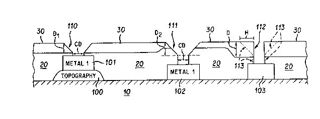
A preferred two-step embodiment of the inventive method
will be described with reference to Figure 3. Via 110 and via
111 are examples of completed vias produced by performing both
steps of this preferred embodiment. The first step of this
preferred embodiment is an anisotropic oxide plasma etch
operation which produces a non-tapered via, such as via 112 of
Figure 3. The first step is preferably timed to have a normal
duration sufficient to extend the ~ia to a normal target depth
(for example, 60% of the oxide layer thickness). Because the
~ -7c- 1313~2~
72094-78
thickness o~ the resist and oxide layer above the target will
typically vary across the wafer, it is desirable to monitor a
~i~
. .
~ l~la~2~ pATENT
--8--
characteristic of the via (such as the thickness of
the material at the via's bottom) during or after
performance of the first step. If the monitoring
operation indicates that the first ~tep has extended
the via to the target, then the second step of this
embodiment of the invention is commenced. However, if
the monitoring operation indicates that the target (a
deeper than normal target) has not been reached, then a
control signal is generated for continuing the first
~tep for a longer than normal duration (or a control
6ignal is ~enerated for repeating the first step) ~o
reach the deeper than normal target.
Preferably, the plasma employed in the first step
consists primarily of CF4, rather than known etchants
such as CHF3, C2F6, or a CHF3/C2F6 mixture. Although a
CHF3/C2F6 mixture has the advantage that its chemistry
is "selective" to silicon (in the sense that it will
erode a silicon embodiment of substrate 10 at much less
rapid rate than it will erode oxide layer 20), we have
found that use of such a CHF3~C2F6 mixture will
undesirably generate an oxide/polymer residue that will
accumulate in the via during the first step of this
embodiment. Such residue will mask the via sidewall
during the second step of this inventive embodiment,
thus inhibiting the econd step. Since CF4 is less
prone to polymerizing reactions than are other etch
chemicals, we prefer to employ a plasma consisting
primarily of CF4 in order to eliminate the problem of
oxide/polymer residue accumulation. Where the via
target is a metal portion (such as portion 101, 102, or
103) deposited on a silicon substrate, rather than at
the substrate itself, use of CF4 (which is not
"selective" to silicon, in the sense that CF4 will not
erode oxide at a greater rate than it will erode
.~,f ," " ,,
~`" 131~ ~2 ~
PATENT
_g_
silicon) i6 not a disadvantage since CF4 will not erode
the metal portion. However, where the via is intended
to terminate directly at a silicon substrate, it may be
preferable to employ an etching chemical (such as CHF3,
C2F6, or a CHF3/C2F6 mixture) which is "selective~' to
silicon, rather than a non-selective chemical such as
CF4, despite the resulting polymer residue accumulation
problem. CF4 is not only non-selective to silicon, but
will in fact erode silicon at a greater rate than it
will erode oxide. Thus, CF4 will seldom be suitable as
a via etching chemical where the via target is a
silicon substrate.
The second step of the preferred embodiment is a
resist erosion tapered plasma etch operation. An
example of the resist and oxide layer material eroded
when such a second step performed on via 112 is the
material outlined by dashed line segments 113. In the
second step, both the resist and the oxide layer are
eroded in a controlled manner so as to produce a via
having a sloping upper portion which traverses the
resist and a portion of the oxide, and a non-tapered
lower portion which traverses a portion of the oxide
layer. The plasma used in the second step is a
mixture Of 2 and CF4. A mixture including CF4 is used
(rather than~a mixture includinq some other
fluorocarbon, such as C2F6) in order to eliminate the
problem of polymer residue accumulation (which residue
may inhibit efficient completion of the second step, or
may inhibit a subsequent metal coating operation). We
prefer that the 02:CF4 ratio should be equal to or
greater than one, so that the resulting sloping via is
free of polymer residue, regardless of the cleanliness
of the etching equipment employed. In one preferred
-` i315~2~
PATENT
--10--
embodiment, we employ a "50%/50%" mixture including
equal parts f 2 and CF4.
The slope of the upper 610ping via portion is
controllable by varying the ratio of oxygen to CF4
employed in the second step. The depth to which the
sloping portion extends is controlled by the duration
of the cecond step.
The cross-sectional profile of a via produced in
this preferred embodiment results in two advantages.
First, the profile permits improved metal coverage of
the via since more metal particles that are sputtered
will arrive at the sloping sidewalls of the upper via
portion than would arrive at vertical sidewalls of a
non-tapered via such as via 112. In the latter case,
the top of the non-tapered via would shadow the
vertical sidewalls.
The second advantage is that the via's bottom
diameter ("CD") will not significantly vary despite:
(a) significant wafer nonuniformities as the via is
etched across the wafer; and ~b) substantial variations
in the duration of the first and second steps as the
via is etched. The duration of the first step may be
varied to ensure that the non-tapered via produced
during the first step will reach the desired targets.
The targets typically will be metal portions such as
portion 101, 102, or 103 in Figure 3, whose depths
below the surface of the resist will in general differ
(for example, as metal portion 101 is at a different
depth than is metal portion 102). This duration
variation may be accomplished by continually monitoring
a characteristic of the via (for example, the
electrical resistance at its bottom) during the first
step, and terminating the first step when the measured
characteristic attains a predetermined value. Despite
-- i31a~22
PATENT
--11--
variations in the first step duration, the diameter of
the non-tapered vias produced in the first step (and
thus the bottom diameter of such vias) will be
substantially uniform. This embodi~ent of the
invention may accordingly be employed to produce vias
having a broad range of aspect ratios, yet having
uniform bottom diameter.
In the second 6tep, the ratio f 2 to CF4 may be
selected to achieve a desired "second ~tep erosion
region" slope (i.e., ratio of the depth D to the
lateral (horizontal) extent H of the "second step
erosion region" bounded by dashed lines 113 of Figure
3), and the second step duration may be chosen to
achieve a desired sloping region depth D. The second
step may thus be controlled so that the bottom diameter
of the via may be left substantially unchanged during
the second step, over a wide range of possible
combinations of depths (D) and slopes (D/H). For
example, only a very thin layer of oxide 20 within
dashed line 113 of Figure 3 is removed from the
vertical sidewalls of the lower portion of via 112
during the second step (so that the via's bottom
diameter is not significantly changed during the second
step), while a much greater volume of resist 30 is
removed from,the upper sidewalls of via 112 during the
second step. Although via 110'8 target (metal portion
101) is shallower than is via lll' 8 target (so that the
first step of the etching operation producing via 110
likely had a longer duration than that producing via
111), and the depth D1 of via 110'8 upper sloping
portion is less than the depth D2 Of via lll's upper
sloping portion, both via 110 and via 111 have
substantially the ~ame bottom diameter CD.
~3~22
PATENT
-12-
The preferxed embodiment described above may be
implemented using a conventional oxide etching device
(such as a commercially available Model GCA 606 unit),
or another conventional plasma etching device having
two-step etch capability. Typical parameters employed
when implementing this embodiment of the invention
using a GCA 606 etching unit are as follows. The first
step i5 performed using CF4 at a gas flow rate of
lO0.00 Sccm, with a chamber pressure of 120 Mtorr; the
6econd 6tep is performed using equal parts Of 2 and
CF4, each at a gas flow rate of 50.00 Sccm, with a
chamber pressure of lS0 Mtorr. The first step is
divided into a first substep (10 seconds in duration)
in which the RF power for the unit is switched off, and
a second substep (18 seconds in duration) in which the
RF power supplied to the plasma i6 430 watts. The
second step is divided into a first substep (lO seconds
in duration) in which the RF power for the unit is
switched off, and a second substep (48 seconds in
duration) in which the RF power supplied to the plasma
is 360 watts.
An alternative three-step embodiment of the
inventive method will be described with reference to
Figures 4 and S. Vias 210 and 211 of Figure 4 are
typical stepped vias of the type that may be produced
by this embodiment of the i~vention. Vias 210 and 211
each have the same bottom diameter CD and opening
diameter D', although they extend to targets 201 and
202 located at different depths Hl and H2 below the
upper surface of resist 30. Thus, stepped vias of the
type shown in Fig. 4 may be produced so as to have a
broad range of aspect ratios, with a uniform bottom
diameter. Because each of vias 210 and 211 is tapered
(i.e., has an opening diameter substantially larger
," j, .. . .
l~t5~2~ PATENT
-13-
than its bottom diameter), more complete metal coverage
(better than 50% coverage) can be achieved using such
vias than could be achieved using non-tapered vias
having the same ~ottom diameter. However, the metal
coverage attainable with vias 210 and 211 is generally
not as complete can be attained with the tapered vias
~such as vias llO and 111) produced in the preferred
embodiment of the invention, because ëach of vias 210
and 211 has vertical sidewalls separated by a
substantially horizontal "step" or "shoulder" at the
interface between resist 30 and oxide layer 20.
Figure 5 shows a typical via produced in
accordance with the three-step alternative embodiment
of the invention, as the via appears after each of the
three steps of this embodiment of the invention. The
first step of this embodiment is an anisotropic oxide
plasma etch operation which produces non-tapered via
300, which extends through resist 30 into oxide layer
20. Preferably, the plasma employed in this operation
consists primarily of CF4, although it may
alternatively consist primarily of a fluorinated
hydrocarbon such as CHF3, C2F6, or a CHF3/C2F6 mixture.
The first step is preferably timed to have a
normal duration sufficient to extend the non-tapered
via to a normal target depth or to a selected distance
above a normal target (for example, 70% of the oxide
layer thickness). As in the embodiment described with
reference to Figure 3, because the thickness of the
resist and oxide layer above the target will typically
vary across the wafer, it is desirable to monitor a
characteristic of the via during or after performance
of the first step. If the monitoring operation
indicates that the first step has extended the non-
tapered via to the target (or to the desired distance
, ...................................... .
13 i ~ 0 2 2 PATENT
-14-
above the target), then the second step of this
embodiment of the invention is commenced. ~owever, if
the monitoring operation indicates that the target (or
desired position above the targetl has not been
reached, then a control signal is generated for
continuing the first step for a longer than normal
duration (or a control signal i6 generated for
repeating the first step).
As in the Figure 3 embodiment, where the target is
a region of a silicon ~ubstrate (rather than a metal
layer deposited on the ~ubstrate), it is desirable to
use an etching chemical (such as CHF3, C2F6, or a
CHF3/C2F6 mixture) which is selective to silicon.
Otherwise, it is preferable to eliminate polymer
residue accumulation in the via by employing CF4 as the
etching chemical, as in the Figure 3 embodiment.
The second step of this embodiment is an isotropic
resist plasma etch operation to erode the resist
surrounding the upper portion of the via, but not to
significantly erode the oxide surrounding the lower
portion of the via. Preferably, the plasma employed in
this second step consists primarily of 2 The result
of the second step is thus to form a stepped via (such
as via 301 of Fig. 5) having an upper non-tapered
portion (having larger diameter D') extending through
resist 30, and a lower non-tapered portion (having
smaller diameter CD) extending into oxide layer 20.
The second step does not significantly extend the total
depth of the via.
The third step of this embodiment is another
anisotropic oxide plasma etch operation which produces
non-tapered via 302, which extends through resist 30
into oxide layer 20 to reach target 304. The plasma
employed in this operation consists primarily of CF4.
~ .
`` i31~2~
PATENT
-15-
As this plasma etch operation is anisotropic, it will
remove oxide volumes 310, 311, and 312 at a relatively
high vertical erosion rate. However, since the
operation's lateral (horizontal~ erosion rate is very
small relative to its vertical erosion rate, it will
not significantly increase the via'6 bottom diameter
(CD~. The third step is preferably timed to have a
nor~al duration sufficient to extend the non-tapered
via to a normal target depth. As described with
reference to the first step, a monitoring operation may
be performed to ensure that the third step is continued
sufficiently long 60 that the ~ia actually reaches the
intended target.
It is well Xnown how to select a relatively high
gas flow rate and low pressure to achieve such
anisotropic erosion during the third step (and the
first step). It is also well known how to select a
relatively low gas flow rate and high pressure to
achieve isotropic erosion during the second step.
It will be apparent to those of ordinary skill in
the art how to modify the three-step process described
with reference to Figures 4 and 5 to etch a multi-
stepped via through a multi-layer coating including
more than two layers. In general, for each additional
layer below the uppermost two layers, it would be
necessary to perform an additional isotropic etch
operation (analogous to the second step of the Figure 5
embodiment) using an etch chemical selective to the
layer immediately above such additional layer, and then
an additional anisotropic etch operation (analogous to
the third step of the Figure 5 embodiment) using an
etch chemical selective to such additional layer.
The embodiment described above with reference to
Figure 5 may be implemented using a conventional oxide
``` 13i5~22
PATENT
etching device (such as a commercially available Model
GCA 606 unit), or another conventional plasma etching
device having three-step etch capability.
The invention also includes a coated semiconductor
substrate of the type shown in Figures 3 and 4, whose
coating has been etched in accordance with any
embodiment of the inventive ~ethod.
The above description is merely illustrative of
the present invention. Various changes in shapes,
sizes, materials, time intervals, and other details of
method and construction may be within the scope of the
invention as defined by the appended claims.