Note : Les descriptions sont présentées dans la langue officielle dans laquelle elles ont été soumises.
13~2~
RCA 84 , 7 3 8
INTEGRATED_MATRIX D I SPLAY C I RCUITRY
This invention relates to integral circuitry for
operating self-scanned matrix display apparatus.
Backqround of the Invention
Many display devices, such as liguid crystal
displays, consist of a matrix of active elements, or
pixels, arranged in vertical columns and horizontal rows.
The data to be displayed are applied as drive voltages to
data lines which are respectively associated with ones of
the columns of active elements. The rows of active
elements are sequentially scanned and the individual active
elements within the addressed row are illuminated in
accordance with the amplitude of the data voltage applied
-to the respective column.
Typically, the flat panel display matrix will
consist of several hundred rows and several hundred
columns. In order to minimize the number of
interconnections to the display it is desirable to
incorporate row and column scanning or multiplexing
circuitry integrally with the display. Currently,
thin-film-transistor (TFT) circuitry is being used by a
number of companie~ to integrate display and addressing
circuitry on common substrates. The materials that are
being used to fabricate the ~FT circuitry are cadmium
selenide (CdSe), polycrystalline silicon (poly-Si) and
amorphous silicon (A-Si).
The advantage of using poly-Si is its high
carrier mobility. Its disadvantages include a narrow
spectrum of useable substrate material, relatively high
leakage currents, and an excessively high proce~sing
temperature.
CdSe has a relatively high carrier mobility and
requires lower temperatures to fabricate (Tmax < 400C).
However, it has proven difficult to produce devices with
uniform parametric characteristics over a display device.
--"` 13 1~
-2- RCA 84, 738
Amorphous silicon is amenable to fabrication at
low temperatures (Tmax < 350C) on a variety of inexpensive
substrate materials. A-Si transistors are simple to
fabricate with uniform parametric characteristics across an
array. However, the carrier mobility (~ < 1 cm2/VS) is at
least an order of magnitude slower than CdSe and poly-Si.
The carrier mobility of A-Si is too slow to permit
construction of scanning circuitry with conventional
designs.
At the current state of the art of integrated
flat panel displays, were it not for its low carrier
mobility, A-Si would probably be the material of choice for
display manufacture.
Scanning circuits for flat-panel display devices
have been fabricated in A-Si using conventional circuit
designs. An example of this type of scanning circuitry in
A-Si is presented in a paper entitled "A~ Active-Matrix LCD
With Integrated Driver Circuits Using A-Si TFTs" by M.
Akiyama et al. in Japan Display '86, Proceedings of the 6th
International Display Research Conference, September, 1986,
at pages 212-215. The device described is a liquid crystal
display incorporating an integral A-Si tapped shift
register with buffer drivers for scanning the rows in the
display matrix. The matrix columns are driven by circuitry
external to the display device. The paper provides
preliminary test results including output voltage waveforms
of the A-Si row scanner. The test data indicates a) that
the maximum frequency of operation is about 30 kHz and b)
that the fall time (i.e. the turn off time) of the shift
register scanner approaches 20 ~ sec even for relatively
small area display devices.
Firstly, while the 20 ~ sec fall time of the row
scanner may be acceptable to develop images, a faster fall
time is more desirable in order to develop sharper images.
Secondly, the 30 kHz frequency limit indicates that a shift
register type of scanning arrangement is incapable of
performing fast data multiplexing for the display column
busses.
'
- 131~3
-3- RCA 84,738
A TFT scanner, for commutating the video signal
to be displayed to the matrix column busses, is illustrated
in the paper "The Design and Simulation of Poly-CdSe TFT
Driving Circuits for High Resolution LC Displays" by
5 I. DeRyche, A VanCalster, J. Vanfleteren and A. DeClercq,
JAPAN DISPLAY '86, Proceedings of the 6th International
Display Research Conference, Septem~er 1986, pp. 304-307.
This scanner was fabricated with the relatively high
mobility material CdSe and includes, a serial-input-
parallel-output data shift register, a plurality of data
latches each coupled to respective ones of the shift
register parallel outputs and associated with a respective
one of the matrix column busses, and a plurality of buffer
amplifiers each of which has an input coupled to an output
of a corresponding latch and an output coupled for driving
a column bus. In this arrangement, the shift register is
coupled to the latches by a first set of gating devices and
the latches are coupled to the buffer amplifiers by a
second set of gating devices.
During a given line period, the data stored in
the latches are applied, via the buffer amplifiers, to the
respective column busses. Concurrently data, or video
signal, for the next line of display is serially loaded
into the shift register at approximately a 6 MHz clock
rate. At the end of a given line period, the data in the
shift register is transferred in parallel to the plurality
of latches. This data is then coupled to the column busses
during the next subsequent line interval.
In light of the speed-performance characteristics
reported by M. Akiyama et al., for shift registers
fabricated with A-Si, it will readily be appreciated that
the commutating circuitry of the type presented by
I. DeRyche et al. cannot be fabricated in A-Si and expected
to operate at the requisite scanning speeds to drive the
vertical columns of a flat panel display device.
Thus, there is a need for commutating circuitry
which can be fabricated in materials having relatively low
~3~5~2~
-4~ RCA 84,738
carrier mobility and which can be operated at relatively
high rates.
Summary of the Invention
The present invention is directed toward latch
circuitry for applying signals to matrix type display
devices. The latch circuitry includes a pair of cross
coupled transistors energized by variable impedance load
devices. The variable impedance load devices are modulated
between low impedance high current modes and high impedance
low current modes to effect factor switching of the latch
circuitry.
Brief Descri~tion of the Drawin~
FIGURE lA is a block diagram of a flat panel
display apparatus including integrally fabricated data
commutating apparatus embodying the present invention.
FIGURE lB is a block diagram of a clock generator
circuit which may be implemented in the apparatus of FIGURE
lA.
FIGURES 2 and 3 are partial block and partial
schematic diagrams of demultiplexing circuitry which may be
implemented in the FIGURE 1 apparatus.
FIGURE 4 is a schematic diagram of latch
circuitry for driving one column bus of the display
apparatus.
FIGURE 5 is a timing graph of the sequence of
operation of the commutating apparatus.
FIGURE 6 i 8 a schematic diagram of alternate
latch circuitry for driving one column bu~ of the display
apparatus.
FIGURE 7 is a timing graph useful in describing
the operation of the FIGURE 6 circuitry.
FIGURE 8 is a schematic diagram of row selecting
demultiplexers and latch driver circuitry.
.. , 13~;~S~
-5- RCA 84,738
FIGURE 9 is a timing graph of the sequence of
operation of the row selection apparatus.
FIGURE 10 is a schematic of an alternate variable
impedance load device
Detailed DescriPtion
The invention will be described in the
environment of a self scanned liquid crystal display
apparatus wherein the active elements are manufactured
using amorphous silicon material. It should be
1~ appreciated, however, that the inventive concepts are
applicable to other types of apparatus reguiring scanning
or commutating circuitry in which conventional scanning
circuitry is incapable of being operated at the desired
speed of operation.
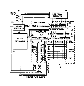
Referring to FIGURE lA, a self scanned liquid
crystal display system is shown in block form. This system
includes a self scanned display array circumscribed by the
broken line 10, and support electronics including a data
signal formatter 24, a master controller 26 and a clock
signal generator 28. The display array 10 includes a
display matrix 12, horizontal scanning circuitry 14 and
data commutating circuitry 18.
The display matrix 10 includes a plurality of P x
Q x R horizontal busses and a plurality of M x N vertical
data lines, where M, N, P, Q and R are integers. A
transistor switch and liquid crystal display element
(pixel) is located at the intexsection of each horizontal
bus and vertical data line. The control electrodes of the
respective transistors are coupled to the horizontal
busseæ. The conduction path of each transistor is coupled
between a liguid crystal display element and a column bus.
The liquid crystal display elements are capacitive elements
and are capable of storing charge, i.e. they will store a
potential. In the operation of this system, a potential is
sequentially applied to the horizontal busses to turn on
the matrix transistors a row at a time. Concurrently with
-6- 13 1 ~ ~ 2 ~ RCA 84,738
a row of transistors being turned on, display data for that
particular row of display el~ments is applied to the column
busses. The display data is coupled to the respective
display element capacitances via the matrix transistors and
then the transistors in the row are turned off. The
display data is stored on the display elements for a frame
period during which time the respective data potentlals
determine the state of illumination or transmissibility of
the respective display elements. After a frame period (the
period required to address all of the hori~ontal llnes) the
horizontal row is again addressed and new display data is
applied to the row of display elements.
Display data to be applied to the matrix is
applied in serial form to terminal 40. This data is
formatted into M parallel signals for application to the
array demultiplexer 19. During each line interval the
demultiplexer 19 converts the M parallel signals into M x N
parallel signals corresponding to the M x N column busses.
Since the demultiplexer converts M signals into M x N
signals, the multiplexer must be capable of switching in,
at most, 1/Nth of a line period. The M x N parallel
signals are coupled to a plurality of M x N input latches
20. These latches are operated so as to minimize the
response time of the demultiplexer.
The demultiplexing of the M parallel signals
representing a line of data and the loading of this data
into the input latches 20 occupies the majority of one line
period.
The data in the input latches 20 are coupled, via
transmission gates 21, to a second plurality of M x N
output latches 22. This coupling is performed in a
relative small percentage of a line period. The data are
stored in the output latches 22 for approximately the next
subseguent line period at which time the data are applied
to the column busses for application to a row of matrix
display elements. The matrix display elements in the
particular row addressed have approximately a full line
period to accept the applied data. Three features of this
131~ ~ ~ 9
data co~mutating arrangement are 1) the number of data
lines which are reguired to be taken off the self scanned
array are reduced from M x N to M; 2) a period of
approximately one line time is available to adjust the data
potential of each array display element; and 3) as will be
demonstrated below, the circuitry may b~ fabricated using
TFT's of relatively low carri~r mobility mat~ri~l ~nd yet
handle tbe relatively fa~t input data rat~
The horizontal scanner 14 include~ a two level
demultiplexer 15, 16 and a latch/driver 17 which includes a
latch driver for each horizontal bus P parallel 3canning
signal~ are coupled to th~ dcmultlple~er 15 In th~
simplest form of operation, th~ P scanning signal~ each
provide a scanning pulse of l/Pth o~ on~ ~ctive framo
interval in mutually exclusiv~ tim~ p~riod- These P
~canning ~ignal~ ar~ converted in dcmultipl~er 15 into P x
R parallel ~canning signals each o~ which provide~ a
~canning pulso of l/(P ~ R)th of on- ~ctiv~ fram~ interval
and which occur~ in mutually exclusiv~ tim~ period~ The P
x R parall~l signals arc coupl~d to th~ demultiple~er 16
which dev~lops P x R ~ Q parall~l scanning ~ignals The
P x R ~ Q parall-l scanning ~ignal~ ~ach provid a scanning
puls~ of duration appro~imating a horizontal lino interval
The~- pul--~ m~y b- con-train d to occur in mutually
oxclu~iv t~ period- or a- will b- d~mon-trat~d b-low
scan pul~ ppli-d to ucco~-iv horizontal row- may
ov rl-p
Th~ P ~ Q x R ~canning pu18-- ar~ coupl~d to
P ~ Q ~ R p~rall-l l~tch/drivor- Tho p~rall-l latch
dr~vor- provid pu-h-pull ~n rgizAtion to th~ horizontal
bu-~ nd aro ~p-cifically d-zign d to bo cap~bl~ o
rapidly turn off of th horizontal bu~
Th ~ast-r controllor 26 provido- multiploxing
control and tranJf r signal- to th colwmn bu~ co~mut-tor
18 nd th horizont~l ~cannlng circultry 14 In addltion,
the ma~t-r controllor provid-D control signal- to tho clock
~ignal genorator 28 which d~v~lop- clocking signals to
enorgize th latch circuit~ 20, 22 and 17 ~ho ~a-t-r
131~9 RCA 84 738
controller may include an oscillator, and logic circuitry
(for example, a microproces~or) for counting pulse~
provided by tho oscillator to generate th~ reguisite
control signals in the appropriate timing relation
For the system to be described, th~ latch
circuits are clocked, during particular time intervals,
with variable duty cycle clocks Clock generator 2a is
configured to provide both constant duty cycle and variable
duty cycle clock signal~
FIGURE lB illustrates exemplary circuitry which
may be implemented for th~ clock generator 2~ This
circuitry includes an o~cillator 31 which generates a
constant freguoncy ~ignal, for e~ampl~, at 10 M~z
Oscillator 31 i~ coupled to a counting circuit 30 which
lS provid-~ asc~nding binary value- for ~ach cycl~ of the
o~cillator ~ignal, for e~ample, th ~equ-nca of value~
0-127 The~e value~ are couplod to th~ addre~ input of a
read only memory (ROM) 32 having 128 me~ory locations
pr-programm~d with logic on- and z-ro valu~- ROM 32
th~r~fore provid - a on or a zoro valu- ev-ry 100
nano-econdJ More p-cifically, ROM 32 i8 programmed to
output, for ~a~plo, a 1 MEz wav orm wh-r-in th- duty
cycl- vari-- ro~ 10 p-rcont to 100 p-rc-nt an~ back to 10
p-rc~nt or a ~-qu-nc- of addr-~ of 1-127 Th- g~neral
~h~p- o~ thi- w~ for~ i~ illu-trat d ~- w~v for~ Ic' in
FIGURE 5 Of cour~-, oth r w~ ah~p-~ ~ay b- programmQd in
th RO~ ~n ~ddition, a~d~tion~l addr aa bit- m~y b-
includ d uch th~t diff rent output -gu-nc-- m~y be
~-1 ct d fro ROM by th- m~t-r controllor Thi- i~
i pli-d by th conn ction d aign~t d MC b-tw n th maJter
controll-r 26 and th addr-~- input of ROM 32 Whon-vor a
varlabl- duty cycl- clock w~v for~ i- d -ir-d, a ro-ot
pul~ appli-d by th ~-t-r controll-r to th r---t
input of th~ count-r 30 to ~t~rt th -qu-nc- at a known
point
Th output of th- ROM 32 i- coupl-d to a delay
l-mont 34 which in thi- xampl- provid - a d lay of 500
nano--cond- Th output signal~ fro~ dolay l-u nt 34 and
~ .
.
~ 31 ~ RCA 84,738
ROM 32 represent two-phase clock signals ~hich are
nonoverlapping at least during the intervals that the clock
duty cycle is less than 50 percent. These two clock
signals are coupled to respective first input ports of
multiplexers 36, 37 and 38. A second pair of two phase
clock signals having a constant duty cycle are coupled to
respective second input ports of multiplexers 36, 37`and
38.
Multiplexers 36, 37 and 38 are controlled by the
master controller 26 to apply either the constant duty
cycle or variable duty cycle clocks to their respective
output terminals. The multiplexer output terminals are
coupled to driver/amplifiers which amplify the respective
clock signals to the appropriate potential values.
The constant duty cycle clock signals are
developed by coupling the output signal of oscillator 3I to
a frequency divider 33 which divides the 10 MHz signal by,
for example, 10 to provide a 1 M~z clock signal. This
signal is coupled to the delay element 35 which delays the
clock signal by, for example, 500 nanoseconds. The output
signals provided by the divider 33 and delay element 35
represent a pair of two phase clock signals.
Refer next to FIGURE 2 which illustrates an
exemplary data formatter which may be used as the formatter
24 in FIGURE 1. The formatter includes a serial-input-
parallel-output shift register 50 and M parallel-input-
serial-output shift registers 52-62. Video data, which
i8 assumed to be in sampled data form and representative
of bilevel bright or dark picture information is applied
in serial form to terminal 40. One line of video data is
composed of M x N samples where M and N are integers. This
video data i8 clocked into register 50 one horizontal line
at a time at the video data rate responsive to clock signal
CLA. Clock signal CLA is synchronized to the video data
rate. After a horizontal line of video data is clocked
into register 50, the line of video data is transferred in
parallel into the M parallel-input-serial-output registers
52-62 responsive to a transfer signal CLB. The parallel
-lo- ~ 31 ~ ~ $~ ~ RCA ~4, 738
transfer operation occurs in a relatively small portion of
a line interval, i.e. in one or two cycles of the video
data rate. After the parallel transfer, register 50 is
conditioned to accept the next occurring horizontal line of
video data.
During the time that register 50 is accepting the
next subsequent line of video data, the ~ parallel~input-
serial-output registers 52-62 read out the current video
data therein to the demultiplexer 19'. Data is serially
read out of the registers 52-62 in parallel, under the
control of clock signal CLC. Since there are M registers
reading out data in parallel, and the video data must be
read out in at most one horizontal line time, the minimum
read out rate of registers 52-62 is approximately N/TH
where TH is a line period, assuming demultiplexing occurs
during an entire line period. The minimum rate of clock
CLC is N/TH, however, as will be demonstrated below, the
frequency of clock signal CLC is actually about twice N/TH.
The respecti~e serial output terminals of
registers 52-62 are coupled to respective serial input
terminals of M, l-to-N demultiplexers MUX(M) - MUX(l)
comprising demultiplexer 19'. In the exemplary system of
FIGURE 2, it is assumed that video data for a horizontal
line is arranged so that first occurring data corresponds
to data for display on the left side of the display and
data occurring last corresponds to data for display on the
right side of the display. After a line of data is loaded
into register 50, the first and last occurring data reside
in the right and left ends of register 50 respectively and,
thus, the firs~ and last occurring video data is
transferred into registers 62 and 52 respectively.
Demultiplexers MUX(1) - MUX(M) are arranged as shown to
apply data to the display column busses from left to right.
Therefore, the data is coupled from registers 62-52 to
demultiplexers MUX(1) to MUX(M) respectively to properly
orient the data for display. Alternatively, if it is
inconsequential whether the information is mirrored about a
vertical axis, or if the video data is input in reverse
~ 3 RCA 84,738
order, then registers 52-62 may be coupled to
demultiplexers MUX(1) - MUX(M) respectively.
FIGURE 3 illustrates, in schematic form, the
configuration of one of the demultiplexers shown in block
form in FIGURE 2. The MUX includes a plurality of thin
film field effect transistors, TFFET ' s, of single
conductivity type, fabricated of low carrier mobility
material (e.g. amorphous silicon). The respective gate
electrodes of the TFFET's are coupled to respective control
lines to which logic control potentials are applied to
condition respective one's of the transistors to conduct to
the exclusion of the remaining transistors. For example,
the control potentials may be provided to sequentially scan
the plurality of transistors so that each transistor is
conditioned to conduct (once per line interval) to the
exclusion of the remainder of the transistors. One
electrode of the principal conduction path of each TFFET is
coupled to the data input terminal, 70, of the
demultiplexer and the other electrode of the principal
conduction path of the respective TFFET is coupled to a
respective one of the output terminals l-N of the
demultiplexer. The particular one of the TFFET's that is
currently conditioned to conduct couples the video data
concurrently applied to the input terminal 70, to its
respective output terminal. The conditioning of particular
TFFET's into conduction occurs at a rate commensurate with
the rate of application of video data to terminal 70, i.e.
the control potentials change at the rate at which
registers 52-62 read out video data.
In order to fabricate the self scanned array with
an expectation of reasonable yield, and in order that
column busses, and ergo pixel elements, have a desirable
pitch, it is necessary to minimize the number of
transistors and interconnecting lines of the array. To
this end, the demultiplexers are designed to provide only
single ended drive to the input latches. Further, because
the latches are driven single ended, and because the
demultiplexers and latch transistors are fabricated with
'.
.
ra ~ 7~ ~
-12- RCA 84,738
low carrier mobility material, the time required to change
the state of the latch is relatively long. In order to
reduce the switching time of the input latch, it is
designed to include a reset transistor to reset the latch
to a preferred state before video data is applied to the
latch. The reset transistor is arranged so that the output
connection to which video data is applied to the la~ch will
be in a high state. Thus, if the video data represents a
high state, the state of the latch is not required to
- 10 change. Con~ersely, if the video data represents a low
state, the state of the latch is required to change.
This arrangement produces the fastest latch state
change for the following reasons. The reset transistor is
coupled to the latch circuit in a configuration such that
it operates in a common source mode to pull down the
potential of an output connection of the input latch rather
than in a source follower mode to pull up the potential of
an output connection of the input latch. Operating in the
common source mode to pull down the potential of the output
connection, the gate-source potential of the transistor
remains constant and, therefore, the current conducted by
the reset transistor to dischaxge the output connection is
substantially con6tant. Conversely, were the reset
transistor operated as a source follower (common drain
amplifier) to pull up the potential of an output connection
of the input latch, the gate-source potential of the reset
tran~istor would decrease as the potential of the output
connection increased, effecting a time dependent decrease
in the current conducted by the reset transistor to charge
the output connection. Thus, for like control potentials
applied to the gate electrodes of reset transistors
operated in the common-source and source-follower modes,
the common-source arrangement will effect faster resetting
of the latch due to its constant current operation.
The demultiplexing transistor is coupled to the
output connection of the input latch opposite the output
connection to which the reset transistor is coupled. Prior
to application of video data to the demultiplexers, all of
.
.' , ~
13~Q~
-13- RCA 84,738
the input latches are reset to the condition wherein the
output connections to which the demultiplexing transistors
are coupled are in a high state. Thus, the demultiplexing
transistors never have to charge the input latches to a
high state, tha~ is the demultiplexing transistors do not
operate in the source follower mode. The demultiplexing
transistors are only required to discharge the output
connection of the input latch on the occurrence of video
data being in a low state and this discharging is performed
in the faster common source mode. Were the input latch not
reset to the foregoing preferred state, the demultiplexing
transistors would be required to alternately operate in the
common-source and source-follower modes for video signals
corresponding to low and high states. Under this set of
conditions, the demultiplexing rate would be limited by the
slower source-follower mode. This in turn would require an
increase in the number of demultiplexers and input data
lines on the self scanned array.
Output latches are included for the following
reasons. The column buffers or drivers are relatively
large devices and present relatively large capacitive loads
to the circuitry driving them. If the column drivers were
driven by the input latches through transmission gates, the
transmission gates would alternately operate in the
common-source and source-follower modes. The time required
of the transmission gates to energize the column buffers in
the source follower mode is too long to provide acceptable
performance. A latch on the other hand, operated with
variable impedance loads, can relatively rapidly drive the
column buffer input capacitance. In addition, the latch
can be arranged to present relatively small input
capacitance, and, thus, may be relatively easily driven
thru the transmission gates. (Note that transmission gates
are required somewhere in the commutating circuitry to
isolate the column busses during the relatively long
intervals that a new line of data is applied to the array.)
FIGURE 4 illustrates the structure of the input
latches, the transmission gates and the output latch and
;
..'...
- .:
.
. . .
-14- ~3~3~2~ RCA 84,738
driver circuitry corresponding to one vertical data display
bus. All of the transistors in the structure are assumed
to be TFFET's fabricated with low carrier mobility material
(e.g. amorphous silicon) and will be referred to
hereinafter simply as FET's. In addition, for descriptive
purposes, the transistors will be assumed to be
enhancement, n-type devices. However, the principals of
operation of the circuitry are not meant to be limited to
field effect devices, but in general, are applicable to
structures employing, for example, bipolar devices.
The input latch includes the cross coupled FET's
104 and 106 having respective source electrodes coupled to
bus 100, drain electrodes coupled to output connections 108
and 110 respectively and gate electrodes coupled to output
connections 110 and 108 respectively. A reset FET 102 has
source and drain electrodes respectively coupled to bus 100
and output connection 108, and a gate electrode coupled to
reset bus 126. FET's 108 and 110 have switched capacitor
load circuits 111 and 117 coupled at output connections 108
and 110 respectively.
The switched capacitor load circuit 111 (117)
includes the serially connected FET's 112, 114 (118, 120)
coupled between the DC bus 126 and output connection 108
(110). A capacitor 116 (122) is coupled between the
interconnection of tran~istors 112, 114 (118, 120) and a
point of DC potential, which for convenience of
illustration, is shown to be bus 126 in the drawing. Input
data is coupled to the latch output connection 110 via a
multiplexing FET 90 (corresponding to, for example, one of
tho transistors illustrated in FIGURE 3) and determines the
state of the latch. The input latch produces complementary
lcgic output states at its output connections 108 and 110
determined by the logic state of the input data or a logic
one potontial applied to the reset bus 124. That is, a
re~et pulse will condition FET 102 to a conducting state,
pulling output connection 108 to a low state and causing
output connection 110 to attain a high state. The high
state at output connection 110 regeneratively conditions
~, .
:
::: , ' :
, , , .
.
~~`` 15 ~3~3~ RCA 8~,738
FET 104 to conduct and latch or hold the circuitry in this
state. Subsequently, if a video sample corresponding to a
high state is applied, via FET 90, to the output connection
].10, the state of the latch will not change.
Alternatively, if a video sample corresponding to a low
state is applied to the output connection 110, this low
state will tend to turn off FET 104. ~
Switched capacitor load circuits 111, 117 are
included to permit varying the gain of the latch. The
series connected FET's 112, 114 (118, 1~0) are alternately
conditioned to conduct by clock signals IC coupled to the
gate electrodes of FET's 112 and 120 and clock signal IC
coupled to the gate electrodes of FET's 114 and 118. When
FET's 112 and 120 are conditioned to conduct, they charge
capacitors 116 and 122 toward the DC potential +V2 applied
to bus 126. Subsequently, FET's 112 and 120 are turned off
and FET's 114 and 118 are conditioned to conduct. During
this time interval the charge stored on capacitors 116 and
122 are coupled to output connections 108 and 110 as
operating currents for the cross coupled FET's 104 and 106.
Textbook switched capacitor theory teaches that
the effective impedance of a switched capacitor structure
similar to FET's 112, 114 and capacitor 116 approaches that
of a resistance having a value of l/Cfc Ohms where fc is
the clocking frequency and C is the value of the
capacitance. The FET's 112 and 114 in the FIGURE 4 circuit
do not have ideal switch characteristics assumed by
switched capacitor theory but the arrangement does produce
a resistive impedance albeit at a different value than
l/Cfc. For a constant frequency on clock signals Ic, Ic,
the resistance value, and thus the gain of the latch
circuit may be varied to greater and lesser values by
decreasing and increasing the duty cycle of the clock
waveforms respectively. The advantage of varying the latch
gain will be described below, after the remainder of FIGURE
4 is described.
The complementary output signals on connections
108 and 110 are coupled to transmission gates 134 and 136
131~
-16- RCA 84,738
respectively. Transmission gates 134 and 136 are
controlled by a transfer pulse Tc applied to their
respective gate electrodes via bus 132. once a complete
line of video data has been multiplexed into the input
latches 20, the transmission gates are conditioned to
conduct and apply the respective output potentials to the
gates of FET's 139A and 139B which form the input circuitry
of the output latches 22'. The transmission gates 134 and
136 are then turned off until the next line interval. The
transmission gates 134 and 136 may be turned off before the
output latch completely changes state provided sufficient
time has elapsed to store the output potentials generated
by the input latch on the inherent parasitic capacitance of
the gate electrodes of FET's 139A and 139B. Thereafter,
even though the transmission gates 134 and 136 are
nonconducting, the stored potential on the gate electrodes
of FET's 139A and 139B will continue to effect a state
change of the output latch 22'.
The output latch 22' includes input FET's 139A,
139B, cross coupled FET's 142, 140 and switched capacitor
load circuits 155, 161. The source electrodes of FET's
- 139A, 139B, 140 and 142 are coupled to the DC bus 138. The
drain electrodes of FET's 139B and 142 are coupled to
output connection 148 and the drain electrode6 of FET's
139A and 140 are coupled to output connection 146.
Switched capacitor load circuits 155 and 161 are
respectively coupled to output connections 148 and 146.
Switched capacitor load circuit 155 (161) includes the
serially coupled FET's 152, 156 (162, 158) and capacitor
154 (160) coupled between the interconnection of the
serially coupled FET's and a point of fixed potential. The
gate electrodes of FET's 152, 156 (162, 158) are
- respectively coupled to clock busses 166 and 164 to which
clock signal6 Dc and Dc are applied for varying the output
latch gain.
The input signal applied to the output latch is
double ended, that is one of the FET's 139A and 139B will
be conditioned to conduct while the other will be
~ 3 ~
-17- RCA 84, 738
conditioned to be non-conducting. FET ' s 139A and 139B are
arranged, when conducting, to pull down the respective
output node to which its drain electrode is connected.
'~hUS, FET ' S 139A and 139B only operate in the faster
common-source mode. Due to the double ended input, output
latch 22' is symmetric and, therefore, need not be reset
before application of input data.
The output latch 22' provides complementary
output signals on connections 148 and 146 which are
respectively coupled to the gate electrodes of FET ' s 168
and 170 configured as a push-pull driver. FET ' s 168 and
170 are serially coupled between relatively positive and
relatively negative DC potentials. The interconnection 172
of FET's 168 and 170 is coupled to a vertical column bus in
the display matrix.
The busses 100, 124, 126, 128, 130, 132, 138,
150, 164 and 166 are common to all of the M x N circuits on
the array.
The system timing is illustrated in FIGURE 5
which timing is based on the following exemplary
assumptions. A horizontal line interval is 64 ~ sec. in
duration of which active video information occupies 60 ~
sec. There are 1024 video data samples per line interval
and a corresponding number of column busses in the display
matrix. The number M of multiplexers a~d of
parallel-input-serial-output registers is 32. The number N
of outputs per multiplexer is 32 and the number of samples
coupled to each of the registers 62-52 is 32.
Since 1024 video samples occur in 60 ~ sec.,
register 50 is clocked at a 17 MHz rate by clock signal
CLA. Thirty-two microseconds are allotted to commutate the
video data via 32 channels, thus, the commutation rate, and
the clocking rate of registers 52-62, (CLC) is 1 MHz.
In FIGURE 5 the topmost waveform designated
serial input video represents the line format of the serial
video data showing two successive lines. At the end of a
line period, a line of video data is loaded into register
50 and respective samples are available on the parallel
-18- ~ 2 ~ RCA 84,738
output connections. A pulse occurs on clock signal CLB
transferring the video data in register 50 to registers
52-62. After this transfer, the registers 52-62 are
clocked in parallel by clock signal CLC providing a 32 ~
sec. burst of 32 pulses of a 1 MHz clock signal. During
this 32 ~ sec. interval, 32 video samples are serially
coupled to each of the 32 multiplexers at the 1 MHz~r~te
and the multiplexer control signals scan the multiplexers
at the 1 MHz rate to couple their respective 32 video
samples to 32 different input latches. About 9 ~ sec.
after the commutating interval the transfer clock, Tc,
provides a pulse of about 9 ~ sec. during which time data
is coupled from the input latches to the output latches.
As indicated before, the input and output latches
are provided with switched capacitor loads so that latch
gain may be varied. Such gain variation is performed twice
per line interval for the input latches and once per line
interval for the output latches. After data has been
transferred from the input to the output latches ~time
intervals designated TI1, TIll, TI21) the input latches are
reset and charged to a preferred state. The resetting or
charging time is enhanced by varying the latch gain. The
latch gain is varied by changing the switched capacitor
loads clock frequency or duty cycle. The blocked waveform
designated Ic, TC represents the input latch clocks, that
is the switched capacitor load clocks. The time intervals
denoted VDC and CDC denote variable gain and constant gain
periods respectively. The gain of the input latches is
also varied during intervals TI3, TI13 immediately after
the commutation intervals TI2, TI12. In between the
variable gain intervals, the clocks Ic, Ic are operated to
provide high gain, that is they are operated at low
frequency or low duty cycle, or alternatively if the
circuits exhibit low leakage currents the clocks Ic, Ic may
be stopped.
The switched capacitor load clocks Dc, Dc of the
output latches are operated to provide variable gain during
timing intervals TIl, TIll, TI21, etc. immediately after
-19- ~ 3 ~ 5 ~ ~ ~ RCA 84,738
the transfer intervals TI4, TI14. In between these
intervals of variable gain the clock signal Dc, Dc are
operated in a constant high gain mode or halted all
together if the level of leakage current permits.
The waveform Sc illustrated in FIGURE 5
represents the potential coupled to the bus 100 of FIGURE 4
which bus provides source potential for the cross coupled
FET ' s 104, 106 . The potential Sc varies between
approximately -2 volts and -5 volts. During the precharge
intervals TIl, TIll, etc., potential Sc is raised to -2
volts to lessen the conductivity of transistor 106 to
lessen the average precharge or reset time of the input
latch. It has been found that the latch gain may be
enhanced, or the latching switching time lessened, by
ramping down the source potential. It is most advantageous
to do this after sample commutation and during the
intervals TI3, TI13, that the input latches are charge
pumped.
The latch operation proceeds as follows. During
reset, potential Sc is set from its operating level of -5
vol's to -2 volts which transition will lessen the
conductivity of both FET's 104 and 106. The reset clock R
is pulsed high turning on FET 102. The potential of the
reset pulse is selected to be large enough so that the FET
102 tends to dominate the influence of FET's 104 and 106.
If output connection 108 is in a low state, it remains low.
Alternatively, if output connection 108 is high, it is
pulled to the -2V potential on bus 100. Concurrently, the
regenerative action of the latch will tend to pull output
connection 110 high. At this time, if the load impedances
of the latch is high, that is, the effective resistance of
the switched capacitor load 111 is large, there will be
little current to support the high potential at output
connection 108, permitting the reset transistor 102 to pull
it down rapidly. Concurrently, the effective resistance of
the switched capacitor load 117 will also be high, and
conseguently will provide little current to pull output
connection 110 high with reasonable speed. Thus, once
-20- 1 31~9 RCA 84,738
enough time has elapsed for output connection 108 to be
pulled low, it is advantageous to condition the switched
capacitor loads to provide lesser resistance or greater
drive current to pull the output connection 110 high.
Thereafter, the switched capacitor loads 111 and 117 may be
returned to the high impedance condition or if the circuit
leakage is sufficiently low, they may be conditione~ to
exhibit substantially infinite impedance by halting the
clocks Ic or IC in the low state. The preferred mode of
operation is to halt the clocks during this interval, i.e.
when video signal commutation is performed. The waveform
designated Ic', TC ' are time expanded waveforms
representing the clocks Ic, IC during the variable
impedance intervals.
After the reset interval, the video signal
commutation begins. The video signal applied to the data
input terminal 70 has exemplary potential values of
positive five and negative five volts for high and low
states respectively. During the commutation period, FET 90
is conditioned to conduct for one microsecond. If the
video signal is high, the latch remains in the reset state.
If the video signal is low, output connection 110 is pulled
toward -S volts, however, in the 1~ sec. commutation
interval, the potential at connection 110 does not attain a
potential much less than -2 volts. First consider that
switch capacitor loads 111 and 117 are operating in the
high resistance state. As connection 110 goes low, output
connection 108 is pulled toward a high state. The one
microsecond commutation time is sufficient to initiate
latch regeneration so that it will continue to change state
even after FET 90 is turned off. Next consider the
preferred mode where the switched capacitor loads 111 and
117 are in the infinite impedance state, i.e. clocks Ic and
Ic are stopped in the low state. If the video input signal
is low, output connection 110 is pulled toward -S volts
through FET gO. With loads 111 and 117 exhibiting infinite
impedance, there is no drive current to support a high
potential at output connection 110, and, thus, it can be
-21- ~ 3 RCA 84, 738
pulled low relatively rapidly thereby shortening the
required commutation time. ~owever, since no drive current
is provided, output connection 108 cannot be pulled high.
Output connections 108 and 110 are both low, but connection
110 is at a lower potential than connection 108 since
connection 108 is clamped at the -2 volts potential SC, but
connection 110 is pulled toward -5 volts. It is not
necessary that connection 110 be pulled all the way to -5
volts. It is sufficient that connection 110 be set to -2.3
volts to insure that the latch attain the desired state
when load current is again applied via loads 111 and 117.
Regardless of whether the switch capacitor loads
are operating in the high impedance state or infinite
impedance state, neither output of the latch will attain an
output potential significantly more positive than zero
volts during the 1~ sec. interval that a -5 volt video
signal is coupled thereto. This represents a power loss
between the demultiplexer input connection an~ the output
connections of the input latch. This power loss is
acceptable because it is in effect traded off against a
bandwidth enhancement.
The bandwidth enhancement occurs in part because
the source potentials of the cross coupled transistors are
raised to -2 volts, thereby lessening the output potential
swing on connection llO that must be effected via
demultiplexing transistor 90 to produce a change of state
of the latch. Secondly, bandwidth is enhanced because
there is little load current to oppose the pull down of
connection 110 via demultiplexing transistor 90. Thirdly,
at least in the preferred mode, during commutation the
cross coupled FET's are effectively removed from the
circuit by the bearing conditions and, thus, transistor 90
is not occasioned to fight any regenerative action of the
latch.
After the completion of the commutation interval
TI2, the input latches enter the charge pump phase TI3 and
the power loss is recovered. At the beginning of this
interval, the switched capacitor loads 111 and 117 are
'
~22- ~ 31~?~ RCA 84,738
conditioned to the high gain state, that is to provide load
current through high effective resistances. At the same
time the source potential, Sc, applied to the cross coupled
FET"S 104 and 106, is changed from -2 volts to -5 volts.
Pulling the potential on the source electrodes of
FET's 104 and 106 to -5 volts conditions FET's 104 and 106
into conduction. The FET having the higher gate potential
rapidly pulls its drain potential low ~and turns the other
FET off) due to the limited load current provided by loads
111 and 117. Alternatively, if the FET having the higher
gate potential cannot pull its drain potential sufficiently
low to completely turn off the other FET, it will still
pull it to a low enough potential to establish the ultimate
state of the latch. About two microseconds are allotted
for this sensing action. Then the switched capacitor
clocks Ic and TC are modulated to provide low load
impedance and high drive current. The output connection
that is conditioned to go high charges relatively rapidly
during this interval, however, it is precluded from
reaching its maximum potential for the following reason.
Refer to FIGURE 4 and assume output connection 108 is to go
to the high state, that is FET's 104 and 106 are to be in
the nonconducting and conducting states respectively. When
the load circuits 111 and 117 are conditioned to exhibit
low load resistance, the ratio of the effective load
resi6tance to the output resistance of FET 106 is too small
to establish the potential at output connection 110
sufficiently low to prevent FET 104 from conducting. The
current conducted by FET 104 prevents connection 108 from
reaching the maximum potential available. Therefore, after
the load circuits 111 and 117 have exhibited the low
resistance or low gain state for several microseconds,
which is sufficient time to charge the respective outputs
to a relatively high potential, the load circuits 111 and
117 are again conditioned to exhibit high resistance (high
gain). In this state, the ratio of the switched capacitor
load impedance to the FET 106 output impedance is
sufficiently high that the potential established on the
~ 3 ~ 3~ 9
-23- ~CA 84,738
gate electrode of the FET 104 is sufficiently low to ensure
that FET 104 does not conduct and its drain electrode can
charge to the maximum available potential.
At the end of interval TI3 the complementary
output voltages of the input latches have substantially
attained their penultimate potentials. These output
potentials are coupled to the output latches by the
transmission gates 134, 136 during interval TI4.
Thereafter, the transmission gates 134 and 136 are turned
off, isolating the input latches from the output latches,
and the input latches undergo the reset operation in
preparation for receiving video data from the next
horizontal line of display data.
The output latches 22' operate in a sensing mode
during intervals TIl, TIll, TI21, etc. and a hold mode
between these intervals. The sensing intervals are
approximately 14~s in duration, during which time the
output states of the output latches may be in transition.
The hold mode intervals are approximately 50 ~sec. in
duration, during which time valid data is applied to the
display matrix. Thus, the display elements have
approximately 50 ~ sec. to accept and store new display
data.
In the sensing intervals, the switched capacitor
loads 155 and 161 of the output latches are modulated to
sequentially provide high load impedances, low load
impedances and then high load impedances to effect fast
state changes of the latches in a manner similar to that
described for the input latches. However, it is
unnecessary to ramp the source potentials of the cross
coupled FET's 140 and 142 of the output latch. At the end
of the sensing interval and during the hold interval the
switched capacitor loads of the output latch are maintained
in the high impedance condition, or infinite impedance
condition if the leakage is sufficiently low, since the
output latch is driving a purely capacitive load (the gates
of the buffer driver).
13~5~?~
-24- RCA 84,738
FIGURE 6 illustrates a preferred embodiment of
the data input structure. The reguisite control signal
~aveforms applicable to the FIGURE 6 circuitry are
illustrated in FIGURE 7. These waveforms can readily be
generated by one skilled in the art of circuit design,
hence the details of their generation will not be
discussed.
The circuitry of FIGURE 6 includes a data input
terminal 70 and a multiplexing FET 90 as in FIGURE 4. The
FET 90 is coupled to an input latch consisting of FET's
601-604 and capacitors C1 and C2. FET's 90 and 601-604
have exemplary channel widths of 50 micrometers. FET's 602
and 603 form a cross coupled latch pair, having respective
source electrodes coupled to the bus VSS1. The drain
electrode of FET 602 and the gate electrode of FET 603 are
coupled to an output terminal 606, and the drain electrode
of FET 603 and the gate electrode of FET 602 are coupled to
a second output terminal 608. Capacitors Cl and C2 are
respectively coupled between the bus BOOST 1 and terminals
606 and 608 respectively. FET 601 has its conduction path
coupled between a dc supply, e.g. 10V, and output terminal
606, and its gate electrode coupled to bus PRCH 1. FET 604
has its conduction path coupled between bus VSS1 and output
terminal 608, and its gate electrode coupled to bus PRCHl.
The operation of the input latch proceeds as
follows. Just prior to the application of video input data
to the data input terminal 70, indicated by the active part
of clock CLC in FIGURE 7, the output terminals 606 and 608
are precharged to, e.g. 10 and 7 volts respectively. This
is accomplished by applying a 15 volt pulse to bus PRCH1
and a 7 volt pulse to bus VSSl. The pulse on bus PRCH1
turns on FET's 601 and 604 which respectively couple 10 and
7 volt potentials to the terminals 606 and 608. FET 602
remains off since its gate-source potential is zero at this
time. FET 603 is biased on since it has a 3 volt
gate-source potential. However, since the potentials at
the source and drain of FET 603 are both 7 volts, FET 603
is non-conducting. After approximately 2-3 microseconds,
-25- ~ 3~a~ RCA 84,738
the potential on bus PRCHl is returned to zero volts
turning off FET's 601 and 604. The 10 and 7 volt
potentials on terminals 606 and 608 are retained thereon by
virtue of charges stored on capacitors Cl and C2. The
potential on bus VSSl is maintained at 7 volts which in
effect removes the FET's 602 and 603 from the circuit.
Subsequent to FET's 601 and 604 turning off, video data is
applied to the data input terminal at a one mega Hertz rate
and respective ones of the multiplexing FET's 90 are turned
on. If the video data coupled to terminal 606 is a high
value, the state of the latch does not change. Conversely,
if the video data is a low value, the potential on terminal
606 is discharged through FET 90, operation in the
common-source mode. Desirably, terminal 606 should
discharge to zero volts, however, it is only necessary that
the potential on terminal 606 be discharged to about a volt
or two below the potential on output terminal 608. In
fact, if the circuitry is realized using
metal-insulator-silicon or MIS Processing, once the
potential on the drain of FET 602 is pulled down to a
potential value which is a threshold potential less than
its gate potential it will conduct between its drain and
bus VSSl, and resist further discharge of terminal 606. It
has been found to be advantageous to cause terminal 606 to
be discharged to 4 volts if the video data is low. Thus,
whether the video data is high or low, a 3 volt
differential will exist between the gate electrodes of
FET's 602 and 603. This potential difference is sufficient
to condition the latch into regenerative action.
After input data has been applied to all of the
input latches (32 microseconds after bus PRCH1 is returned
to zero volts) bus VSSl is returned to zero volts (see
FIGURE 7). At this point the FET 602 or 603 having the
greater drain potential conditions the gate of the opposite5 FET to begin discharging its respective output terminal.
once bus VSSl is returned to zero volts, bus
BOOST 1 is energized with a ramped voltage having a slope
of approximately 3 volts per microsecond and a terminal
-26- 13 ~ 3~2 ~ RCA 84,738
value of approximately 10 volts. This voltage is coupled
to terminals 606 and 608 via capacitors Cl and C2
respectively. A virtual constant load current, CQV/~t, is
thereby coupled to the latch output terminals to pull the
requisite output terminal to a high potential, where ~V/~t
is the rate of change of the potential on bus BOOST 1. The
opposite output terminal is discharged through the
regenerative action of the latching FET's 602 and 603. Bus
BOOST 1 is held at its terminal high voltage until the
input latch is again precharged to accept new data for the
subsequent ~ideo line.
Output terminals 606 and 608 are coupled to
inputs of transmission gates 640 and 642, which in this
case are a type of NAND gate. Transmission gate 640 (642)
consists of the serially connected FET's 610 and 612 ~614
and 616) between ground potential and output terminal 626
(628) of output latch 600. The gate electrodes of FET's
612 and 614 are coupled to output terminals 606 and 608
respectively. The gate electrodes of FET's 610 and 616 are
coupled to bus TC. When bus TC is pulsed high, FET's 610
and 616 couple the source electrodes of FET's 612 and 614
to ground potential. Since output terminals 606 and 608
provide complementary output potentials, one of FET's 612
and 614 will be conditioned to conduct and establish the
state of the output latch 600.
Output latch 600 includes a cross coupled pair of
FET's 618 and 620 having respective source electrodes
coupled to bus VSS2 and respective drain electrodes coupled
to output terminals 626 and 628 respectively. -A second
pair of FET's (622 and 624) are respectively coupled
between a point of positive potential (e.g., 10 volts) and
output terminals 622 and 624, and have their respective
gate electrodes coupled to bus PRCH2. The FET's 610-624
have exemplary channel widths of 100 micrometers. In
addition, capacitors C3 and C4 are coupled between bus
BOOST2 and output terminals 626 and 628. In operation,
output latch 600 is first precharged and then data is
applied. Precharging is performed at a time such that the
-27- 1 3 ~5 ~ 2 ~ RC~ 84,738
output latch will be ready to accept new data shortly after
new data is stablized in the input latch. Precharging is
initiated by applying a pulse (for example lSV) to bus
PRCH2 and turning on FET's 622 and 624. In addition, a
pulse of 10 volts is applied to bus VSS2. As shown in
FIGURE 7, this occurs shortly after the potential ramp on
bus BOOSTl reaches its terminal potential.
FET 's 622 and 624 charge output terminals 626 and
628 to 10 volts in approximately two microseconds. Bus
PRCH2 is then returned to ground potential. FET's 618 and
620 are non-conducting since their ~ate, drain and source
potentials are all at 10V. After bus PRC~2 is returned to
ground potential, bus TC is pulsed for about two-three
microseconds and one of FET's 612 and 614 will discharge or
partially discharge one of the output terminals 626 and 628
in accordance with the state of output terminals 606 and
608 of the input latch. Since no load current is supplied
to output terminals 626 and 628, they may be rapidly
discharged. The potential on bus TC is then returned to
ground after which the bus VSS2 is returned to ground,
biasing one of FET's 618 and 620 into conduction and
initiating regenerative action in the output latch 600. At
this point a ramped voltage is applied to bus BOOST2 to
provide effective load currents to the latch output
terminals and raise the output potential of the terminal
determined to be in the high state. The potential applied
to bus BOOST2 iB similar in slew rate and terminal value
tothe potential applied to BOOST1. The potential applied
to bus BOOST2 i8 held at its terminal voltage (100) until
theprecharge cycle is reinitiated at which point it is
returned to ground potential.
The time, ~0, required to precharge the output
latch and complete a state change of the output latch is
approximately 10 microseconds. Stable output data is
therefore available for 54 microseconds per line (row) of
data.
Output terminals 626 and 628 are coupled to the
gate electrodes of FET's 630 and 632 which form a push pull
,
" ' ' ' ~
-28- 131~2~ RCA 84,733
driver stage Exemplary channel widths of FET's 630 and
632 are 800 micrometers
As configured ln ~IGURE 6, ~he c1rcultry lnverts
the video signal. This invorsion can be elimlnated by
reversing the relatively negative and relatively positive
bus connections to FET's 630 and 632
The commutat1ng system as described is Li~lted to
applylng two level video brightness signalc to the display
device This system has application in integrated displays
exhibiting grey scale at least in the following context
T Gielow, R Hally, D Lanzinger and T Ng in a paper
entitled "Multiplex Drive of a Thin-Film EL Panel",
published in the May 1986 SID Internation 1 Sy~posium,
Digest of ~echnical Papers (pages 242-244), and G G
Gill~tte et al in U S Patcnt 4,766,430 entitled
"Display Device Drive Circuit", which issue~ on A~u~t 23,
1988, de~cribe drive circuits for a matrix display
d~vice which includcs a counter for each column of the
diYplay The counters are set with brigh~ness count values
to e~tabli~h grey ~cale potential~ for the pixel~ These
counter~ are coupled to tran~fer gat~ which reQpectively
couple an analog voltage ra~p to all of the column busses
Th- rosp-ctivo counters turn off thoir corre~ponding
tran~f-r gat~- wh~n tho ramp voltag~ corre~ponds to the
valu- in th~ counter The-e a~alog valu-l ar~ ~tored on
tho bu- capacit nc0~ for th- duration of tho line interval
and aro av~ilabl- for ~etting tho potontial of th- pix~l
el-~ont~ Th commutating circuitry d~-cribed her~in may
b- iqplom~nted to apply th~ r~gui~it- binary brigh~ness
cou~t valuo- to th~ count~r circuit-, which brightne~s
count valuo- corr~pond~ to video signal
F~GUaE 8 ~how~ the row 0-1ect circuitry for one
row bur This circuitry includos a portion of th- l-to-R
d~mul~iplo~-r 15' and th~ l-to-Q do~ultiple~er 16' each of
which ar- con-truct~d similar to tho d-multipl-x-r ~hown in
FIGURE 3 ~f the number of row bu~ a-~um~d to be 512
then th~ first lev-l domultiplexer 15~ may consi~t of eight
1-by-8 demultiplexers and the second lovel demultiplexer
J~" ` .
29 13~ RCA 84,738
16' may consist of sixty four 1-by-8 demultiplexers. With
this arrangement, the number of address connections
necessary to address 512 row busses is 24 (i.e. three times
eight). Note where system speed is not the critical
parameter the two level demultiplexer may be replaced by a
shift register scanner. But even where speed is not
critical, the two level demultiplexer provides advantages
over a shift register scanner in that it permits addressing
the row busses in any arbitrary sequence where a shift
register scanner does not.
In FIGURE 8, the box designated 15' is meant to
represent a portion of one of the eight 1-by-8
demultiplexers of the first level demultiplexer 15. The
box designated 16' is meant to represent a portion of one
of the sixty four 1-by-8 demultiplexers of the second level
demultiplexer 16. Three of the eight switches are shown in
the demultiplexer 16', which switches are coupled
respectively to three successive latch/drivers 17', 17" and
17"'. The details of latch/driver 17" are shown in
schematic form and is seen to resemble the input data
latches, except that the output connections 208, 210 of the
latch driver 17" are coupled directly to the gate
electrodes of driver FET's 268 and 270 respectively.
The basic operation of the latch driver 17" will
be described with reference to the waveforms of FIGURE 9
wherein the topmost illustration designated TI corresponds
to the timing intervals illustrated in FIGURE 5.
A desirable criterion of operation is that the
pixel FET~s be turned off rapidly at the end of a line
interval, that is before data on the column busses changes.
This rapid turn off is effected by conditioning reset FET
202 to rapidly change the state of the latch/driver from
the on state to the off state in concert with changing the
load impedance of the latch. RESET FET 202 is pulsed on by
a reset pulse either just prior to the timing interval TI4
when video data is transferred from the input to the output
data latches, or during the early portion of TI4, before
any significant data transfer has taken place.
-.:
-
.
:
`2 ~
-30- RCA 84, 738
The latch/drivers are operated with variable
impedance loads similar to the input data latches. It is
convenient to reset the latch/drivers during the interval
TI3, TI13 in order to share the variable load control
clocks Io, Io with the data latches. The reset pulses, RR,
in FIGURE 9, are shown coincident with the intervals TI3,
T113 for this reason.
Reset FET 202 is coupled tO output connection 210
and desirably operates in the common-source mode to pull
connection 210 low. If this is to turn the driver stage
(268, 270) off, then the drain connection of FET 270 is
coupled to a relatively positive potential W2 and the
source connection of FET 268 is coupled to relatively
negative potential W 1.
The reset pulse RR is coupled in common to all of
the latch~driver circuits during each line interval.
Therefore, the latch output connection 208 of each
latch/driver is high at the beginning of each line
interval. ~ latch/driver is conditioned to the on state by
pulling the latch output connection 208 low. This is
effected by concurrently conditioning FET's SQn+1 and SRn+
into conduction and conditioning the PK select line to a
low state. The conditioning pulses are shown as Qn+1~ Rn+
and PK in FIGURE 9. The latch/driver output waveforms for
latch/drivers 17', 17" and 17"' are illustrated as RBn,
RBn+1 and RBn+2 respectively.
In this mode of operation the select pulses Q, R
and P are applied to initiate a state change, after the
reset operation, in the latch/driver addressed. At this
time, (TI4, TI14,) the variable impedance load circuits 211
and 222 of the latch circuits are in the high impedance
state so that the demultiplexer FET's can rapidly pull
output connection 208 low. The load circuits are then
conditioned (TI1, TI11) to generate with variable rate
clocks to rapidly charge the output connection 210 to its
maximum output drive potential. The select pulses Qi' Ri
and Pi need not be applied for the entire line interval,
but only long enough to effect a state change.
~3~2~
-31- RCA 84,738
When the latch/driver is subsequently reset by
reset transist~r 202, the variable load impedances are
similarly sequenced from high to low to high impedance
states to reduce the latch/driver reset time.
The aforedescribed mode of row selection requires
that the latch/driver currently addressed switch from
low-to-high and then high-to-low in one line time. The
time required for these two transitions limits the amount
of time available to perform a data change at the pixel
elements. It is possible, with little noticeable affect on
the information displayed, to perform a row select one (or
more) line periods in advance of the normal row select and
to hold the row bus high for two (or more) line intervals
instead of one. (Note that the resultant data in a row of
pixels is determined at the instant the row bus is turned
off.) This mode affords the pixels substantially a full
line inter~al to accept new data.
In this mode of operation, the reset transistors
202 cannot be used and the latch/drivers must be both set
and reset via the demultiplexers. Since resetting (turning
off) the latch/driver is more critical than setting
(turning on) the latch/driver, the demultiplexer FET's
operate in the source follower and common source modes to
set and reset the latch/driver respectively. During the
setting and resetting intervals, the latch load impedances
are modulated as in the previous example. The only change
reguired of the circuitry is that potential W 1 be made
relatively positive and potential W2 be made relatively
negative. In addition, the select pulses Qi and Ri must be
applied during the set period and again during the reset
period and the select pulses Pi must alternate between set
(positive) and reset (relatively negative) potentials.
Waveforms illustrating this operation are illustrated with
primes in FIGURE 9. In the illustrated example, each line
row is conditioned to an "on" voltage for approximately two
line intervals. This may be extended to larger numbers of
line intervals with appropriate selection of address
signals P, Q and R.
:
': - , ' , :
: .
' ~
.: , . . .
1 3 ~
-32- RCA 84,738
If 512 lines of data are processed in an
interlaced manner of 256 lines per field, the data may be
displayed in a psuedo non-interlaced form by applying each
li~e of data to t~o lines of display elements. For
example, duxing odd fields, rows 1 and 2, 3 and 4, 5 and 6,
etc., may be respectively energized concurrently. Then
during even fields rows 1, 2 and 3, 4 and 5, 6 and ~, etc.,
are respectively energized concurrently.
The exemplary circuits disclosed in FIGURES 4 and
8 include switched capacitor circuits as variable load
devices, however, other variable load circuits may be
substituted therefore. For example, a single FET may be
substituted for the switched capacitor circuit and the gate
potential varied. This FET is sized such that for a gate
potential sufficiently high to provide the desired
penultimate latch output potential, the source-drain
impedance will correspond to the high impedance state. To
develop the low impedance state a greater gate potential is
applied. FIGURE 10 illustrates a further variable
impedance load circuit which may be substituted for the
switched capacitor circuits. This load circuit consists of
two parallel connected FET's 300 and 302 which would be
connected between, for example, bus 126 and output
connection 108 in FIGURE 4. FET 300 has a constant DC
potential applied to its gate electrode, and provides a
high impedance resistance to the latch via its drain-source
conductance path. FET 302 iB configured to have lower
drain-source resistance and is conditioned to conduct in
parallel with FET 300 during intervals that low load
impedance is reguired.