Note : Les descriptions sont présentées dans la langue officielle dans laquelle elles ont été soumises.
~ 3~S ~2~
.
-- 1 -- .. .
1 THIN FI~M MOS TRA~SISTOR HAVING PAIR OF GATE EL~CTRO~ES
2 QPPOSING ACROSS 5EMICONDUTOR LAYER
4 BACKGROUND OP THE INVENTION
Field of the Invention_
6 The present invention relat s generally to a
7 MOS trAnsistor. More specifically, the invention
8 relates to a MOS transi~tor which h~s a pair ~f
9 electrodes opposing across a semiconductor layer.
Further p2rticul~rly, the .invention relates to ~ thin
11 film MOS tr~nsistor which may h~ve enhanced electrQn
1~ mobility.
3 RIEF DESCRIPTION OF THE DRAW MGS
4 The present invention will be understoD~ more
ully from the detailed descrîption given herebelow and
6 from the accompanying drawings of the preferred
7 embodiment sf the invention, which, howeverl sh2uld not
8 be taken .to limit the invention to the specific
9 embodiment but are for explanation and ~nderstanding
only.
11 In the drawings:
12 Fig. 1 is an energy level diagram of the
13 conventional MOS transistor;
14 Fig. 2 is a sectional view of tbe first
embodiment of ~ thin film MOS transistor ~ccording to
16 the pre~ent invention;
17 Fig. 3 is a gr~ph ~howing relationship between
lB thickness of ~ctiv~ layer ~nd drain Gurrent in MOS
19 transis~or;
~ig o ~ is an energy level diagram of the first
21 embodiment of the MOS transistor of Fig. l; and
22 Fig. 5 is a sectional view o~ ~he second
23 embodiment of the thin film MOS transistor according to
24 the present invention.
~` 13~2i
- 2 -
13 .Description o~ the Backqround Art
14 Convention~lly, ~uch type of thin film MOS
lS trnnsistors ~re provided pairs of g~te eleGtrodes
1~ opposing across semioonductor layer. In general, the
17 semiconductor layers formed between ~he gate
18 electrodes constitute thin film in ~ range of 3,000 nm
~9 to 5,000 nm. Eneryy l~vel diagram o~ typical thin film
20 MOS transistor is shown in Fig. :L.. As will be een
21 from the enersy level Ec at the end of energy trans~er
22 path ~s illustr~ed in Fig. 1, lateral gr~dient of
23 transfer band over the nergy transfer p~tp tends to
2~ b come su~stantial. This is caused by local
concentration of electron path on the ~urf~ce of a
26 channel. Thi~ cau~es nDrrowing of the electron path on
27 the channel surface and th~s causes seatter.ing o~ free
28 elec~ron to lower mobility ~ of electron.
2g As will be ~ppreciated, the mobili~y ~ of
electron is one of the principle fa~tor for determining
31 the performance of this type transi~torl especial1y for
32 operational ~peed of the tr~nsistor. On the other
33 hand, requirement for higher oper~tional speed
34 tr~nsistors becomes higher ~or widening ~pplication of
3~ ~uch semiconductor transistors. In this view, the thin
36 film M05 transistors ~re required higher electron
~ ~ 3 ~ 2 ~
.,
1 mobility.
2 SUMMARY OF IH! INVenTIDN
3 Therefore, it is 3 principle object of the
4 present invention to prsvide a thin fil~ MOS transi~tor
with satisfactorily high electron mobility.
6 Another object of the invention is to provide
7 ~ thin film MOS ~ransistor which has nn improved
B 9eometry making ea~y to align compon2nts.
9 In order to accomplish the ~forementi~ned and
other objects, a ~hin ~lm MOS trAn5istor, according to
11 the pre5ent invention, has a c~nstruction which can
12 minimize scattering of electron an~ thus maximize
13 electron mobility for ~llowing higher ~peed operation
14 of the.transis~or. Toward this, the MOS ~r~nsistor has
a thin film form ~emiconductor layer having a thickness
16 in a xange less ~han or equal to 100 nm, between a pair
17 of gate electrodes which oppose to each other across
18 the ~emiconduc~or layer.
19 ~ According to one aspect of the invention, a
thin film MOS transis~or. comprises a fir~t gate
21 ~lectrode formed on ~ ubstrate a oemiconductor active
22 layer~ormed over ~he first g~te elec~rode ~nd opposing
23 to the latter via a first~insul~ting l~yer ~nd defining
24 sour~ce, dr~ain and ~ channel regions, the ~hannel region
~eing force be~ween the source and drain regionsj and
26 which ~ctive layer has a thickness in ~ range less than
27 or eq~al to 100 nm, ~nd a se~ond g~te electrode forme:d
28 ov~r the active loyer ~nd opposing to the latter vi~ a
29 second in~ul~ing l~yer.
:30 . The second insulating l~yer is preferably
31 thinner th~n.the first insulatin~ layer. The first and
32 second gate el~ctrodes~and the channel region o~ the
33 active layer are arranged su~stantially in ~lignment.:
34 - In the pr~ctical construction, ~the ~ctive
Iayer is formed o~ polycrystalline silicon.
36 The ~ir~t and second gate electrodes are
, i., j ~ _ ,,
1 practically arranged ~t opposite sides o~ the active
2 layer. The first gate electrode may be so arranged as
3 to establish substantially smaller input capacity than
4 that established by the second elect,rode. The ~irst ~ate
~ electrode may have ~ fir~t g~te length shorter than a
6 second gate length o~ the second 031:e electrode.
7 Accordin~ to another aspect ~f the invention,
B a thin film MOS transistor comprises a ~irst gate
9 electrode ~ormed ~n ~ substr~e and having a first gate
10 leng~h, a second gate electrode ~pposing to the first
: 11 gate electrode, the ~econd gate elec.trode having a
12 second gate length longer than the first length of the
13 first gate.electrode, the second gate electrode being
1~ arr~nged substantially in alignment with the first
electrode, and a ~emiconductor active layer formed
16 between the first ~nd second gate electrodes and
17 defining source, drain ænd a channel regionsj the
18 channel re~ion being d fined between the source and
19 drain regions and ~pposing to the first gate electrode
Yia a first insula~ing:laye~ ~nd to the second 98te
21 electrode via ~ second insulating layer, and the active
22 layer h~ving a thickness in a r~nge l~ss than or eq~al
23 So 100 nm.
24 According to a still further aspect ~f the
invention, a thin film MOS transistor comprises a first
26 gate el~ctrvde formed on;a substrate and having a first
27 g~te length, a ~econd gate electrode opposing to the
28 ~irst gate el~ctrode, the secon~ gate cl~ctr~de having
29 a second g~te length l~nger th~n the firs~ length of
the. first gate electr~de, the sec~nd gate electrode
31 being arranged ubstantially in ~lignment with the
32 first electrode, and a semiconductor ~ctive layer
33 formed between th~ first and ~ec~nd:g~te electrodes and
34 defining source, drain and ~ channel regions, the
channel regivn being defined between the source and
36 dr~in regions and opposing to the ~irst gate electr~de
.
13~ ~21
.
- 4A
1 via ~ first insul~ting l~yer ~nd to the ~econd gate
2 ele~trode vi~ a second insul~ting layer.
DESCRIPTION OF TH~ P~EFE~ E~ E~FNr
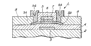
26 Referring now ~o the drawi.ngs, paricularly to
27 FiyO 2~ the ~izst embodiment of a thin ~ilm MOS
2R tr~nsistor, aocording to the present invention, is
29 generally referred to by ~he reference numer 1 'il".
~he MOS transistor 1 has a substr2te 2 which is ~nade of
31 quartz. A gate electrode 3 of polycrystalline silicon
32 is formed on the quartz substrAte 2. The
33 polycrys~alline silicon gate elPctrode 3- will be
34 hereinafter referred to as "first gate electrode". An
insulation layer 4 of silicon dioxide (SiO~) is formed
~ ~ver the quartz subs~rate surf~ce ~nd over the
2~
1 polycrystalline silicon gate electrode 3.
2 An active layer 5 of semiconductor layer is
3 formed on the surface of the silicon dioxide insulation
4 layer 4. In the shown embodiment, the semiconductor
i 5 active layer 5 is formed of polycrystalline silicon, by
6 way of chemical vapor deposition and other appropriate
7 process. The thickness of the semiconductor active
8 layer 5 is in a range oE less than or equal to 100 nm.
9 Though the shown embodiment of the thin film
MOS transistor employs polycrystalline silicon -to form
11 the semiconductor active layer, any other ma-terial
12 appropriate to use, can be used for forming the
- 13 semiconductor active layer. For example,
14 monocrystalline silicon can be used in place of the
polycrystalline silicon for forming the semiconductor
16 active layer.
17 In the shown embodiment, the semiconductor
18 active layer 5 is formèd as P-type layer. N type
19 impurity i5 doped at both lateral end portions of the
semiconductor active layer for forming a source region
21 5A and a drain region 5B.
22 A gate insulation layer 6 and a gate electrode
23 7 are formed on the semiconductor active layer 5. The
24 gate electrode 7 will be hereinafter referred to as
"second gate electrode". The gate insulation layer 6
26 is formed of silicon dioxide. On the other hand, the
27 second gate electrode 7 is formed of polycrystalline
28 silicon. These silicon dioxide gate insulation layer 5
29 and the second polycrystalline silicon gate electrode 7
are arranged on the semiconductor active layer 5 in
31 alignment with the first polycrystalline silicon gate
32 electrode 3. As will be seen from Fig. 2, the
33 thickness of the silicon dioxide gate insulation layer
34 6 is thinner than that of the insulation~layer 4.
Therefore, the distance between the second
36 polycrystalline silicon gate electrode 7 to the opposing
~ 13t~2~
~ 6
1 surface of the semiconductor active layer 5 is set
2 smaller than that between the first polycrystalline
3 silicon gate electrode 3 and the opposing surface of
4 the semiconductor active layer 5. As a result, the
working function of the second polycrystalline silicon
6 gate electrode 7 become greater than that of the first
7 polycrystalline silicon gate electrode 7.
8 As far as the electron mobility is concerned,
9 even distance between the gate electrodes and the
active layer may exhibit equivalent performance to that
11 of the shown embodiment. However, the shown
12 arrangement of the gate electrodes relative to the
13 active layer is preferred for malntaining the input
14 capacity level equivalent to single gate type MOS
transistor. This can be achieved by setting the input
16 capacity created by the first gate electrode small by
17 providing greater distance to the active layer.
18 Additionally, the MOS transistor 1 has an
19 insulation layer 8 and aluminium electrodes 9A and 9B
for external conn~ction. The aluminium electrodes 9A
21 and 9B are respectively connected to the source region
22 5A and the drain re~ion 5B of the semiconductor active
23 layer.
24 Fig. 3 shows~ variation of drain 'current in
relation to the thickness of the semiconductor active
26 layer. In Fig. 3, line A shows variation of drain
27 current when the second polycrystalline silicon gate
28 ~ electrode 7 is solely used; line B shows variation of
29 drain current when the first polycrystalline silicon
gate electrode 3 is~solely used; and line C shows
31 variation of drain current when both gate electrodes
32 are used. With respect to the line C, it will be
33 appreciated that when both of the first and second
34 polycrystalline silicon gate electrodes 3 and 7 are
used, the drain current become greater than the sum
36 value of drain currents obtained when each one of the
~ 3 ~
1 second and first polycrystalline silicon gate
2 electrodes is solely used, in a range of thickness of
3 the semiconductor active layer 5 less than or equal to
4 100 nm. This means when both gate electrodes are used
in combination, greater current t:hat the sum value of
6 the currents flowing through channels respectively
7 formed on the active region solely by one of the second
8 and first polycrystalline silicon gate electrodes 7 and
9 3. This results from mutual influence of electric
fields formed around both second and first
11 polycrystalline silicon gate electrodes to increase
12 electron mobility ~ in the channel.
13 Fig. 4 is energy level diagram of the shown
14 embodiment of the MOS transistor showing lateral energy
level Ec distribution. As seen, the line Ec
16 representiny the energy level approaches the
17 Fermi-level EF shown by broken line and become close
18 to flat. By this, electron mobility ~ ahd mutual
19 cond~ctance gm is increasedO In Fig. 4, line Ei
represents center of forbidden band.
21 As will be appreciated herefrom, since the
22 shown embodiment of the thin film transistor according
23 to the invention, is successful to provide
24 satisfactorily high electron mobility and thus to make
the MOS transistor applicable for LSI.
26 Fig. 5 shows the second embodiment of the thin
27 film MOS transistor, according to the invention. The
28 constructional components of MOS transistor of the
29 shown embodiment are represented by the same reference
numerals to that of the former embodiment and neglect
31 detailed discussion.
32 The shown embodiment features a novel geometry
33 which allows easy alignment of the first and second
34 polycrystalline silicon gate electrodes 3 and 7. In
the shown embodiment, the second polycrystalline
36 silicon gate elect~ode 7 has a gate length ~2. On the
:. .
- :~3 l5~2~
-- 8
1 other hand, the first polycrystalline silicon gate
2 electrode 3 has a gate length ~L which is shorter than
3 the gate length ~2 of the second polycrystalline
4 silicon gate electrode 7.
In production, the semiconductor active layer
6 5 is formed in self-alignment with the first
7 polycrystalline silicon gate elect:rode 7. Therefore,
8 even when the irst and second polycrystalline silicon
9 gate electrodes 3 and 7 mutually offset to off cent r
the each otherS the first polycrystalline silicon gate
11 electrode can be maintained beneath the second
12 polycrystalline silicon gate electrode and beneath the
13 region (channel region) between the source and drain
14 regions 5A and ~B of the semicond~ctor active layer 5.
Therefore, the first polycrystalline silicon
16 gate electrode 3 will never placed in a position
17 partially or in whole opposing to one of the source and
18 drain regions 5A and SB. This minimize parasitic
19 capacity to be created between the first
polycrystalline silicon gate electrode and one of the
21 source and drain regions. Therefore, element
22 characteristics o the MOS transistor can be maintained
23 acceptable.
24 Furthermore, since the shown geometry does not
2S require substantial precision in fabrication,
26 ~production of such MOS transistor become easier with
27 substantially high yield.
28 Therefore, the invention fulfills all of the
29 objects and advantages sought therefor.
While the present invention has been disclosed
31 in terms of the preferred embodiment in order to
32 facilitate better understandin~ of the invent~ion, it
33 should be appreciated that the invention can be
34 embo,died in various ways without departing from the
principle of the invention. Therefores the invention
36 should be understood to include all possible
"~ ` `; .
~.3~ 2~
g
1 embodirnents and modificatiorls to the shown embodiments
2 which can be embodied without departing ~rom the
3 principle of the i.nvention set out in -the appended
4 claims.
.