Note : Les descriptions sont présentées dans la langue officielle dans laquelle elles ont été soumises.
1 31 7674
The present invention relates to an optical
pickup device that can be used in information-reproducing
apparatus such as a compact disc reproducing apparatii,
video disc reproducing apparatii and the like.
5In the accompanying drawings, which illustrate
embodiments of the invention as well as certain
conventional devices:
Figure 1 is a side view showing the fundamental
structure of an optical pickup device of the present
invention;
Figures 2(a), . 2(b) and 2(c) are schematic
diagrams showing the relationship between a hologram
optical element and a photodetector 7 with five divided
regions shown in Figure 1;
15Figure 3 is a side view showing a conventional
: optical pickup device;
Figures 4(a), 4(b) and 4(c) are schematic
diagrams showing the relationship between a hologram
optical element and a photodetector with six divided
regions shown in Figure 3;
Figure 5 is a side view showing another
conventional optical pickup device;
Figures 6(a), 6(b) and 6(c) are schematic
diagrams showing the relationship hetween a hologram
optical element and a photodetector with six divided
regions shown in Figure 5;
Figure 7 is a side view showing the fundamer.tal
structure of another optical pickup device of the present
invention; and`
30Figures 8(a), 8(b) and 8(c) are schematic
diagrams showing the relationship between a hologram
~ optical element and a photodetector 37 with five divided
-~ regions shown in Figure 7.
,~ .
Turning now to Figure 3 of the dra~ings, a
: 35 conventional optical pickup device is shown that has a
semiconductor laser 11, a grating 12, a hologram optical
1317674
element 13, a collimating lens 14, and an object lens 15.
A light beam from the semiconductor laser 11 is diffracted
by the grating 12, resulting in three separate beams, one
of which is the zero-order diffracted beam (below re~erred
to as the main beam), and the others of which are the
first-order diffracted means (below referred to as the sub-
beams) in the positive and negative directions that are
substantially orthogonal to the plane in Figure 3. These
three separate beams are further diffracted by the hologram
optical element 13. The resulting zero-order diffracted
beam of each of the above-mentioned separate beams enters
the object lens 15 via the collimating lens 14 and is
focused on a recording medium 16. When the main beam is
focused on a pit of the recording medium 16, the intensity
of the beam reflected from the recording medium 16 gives a
pit signal. The two sub-beams, which are positioned
symmetrically with respect to the above-mentioned main
beam, are focused on the recording medium 16 in such a way
that they shift to a larger extent in the tracking
direction of the recording medium 16 and to a small extent
in the radial direction of the recording medium 16, thereby
generating a tracking error signal from a difference in the
intensity between the two sub-beams reflected from the
: recording medium 16. The beams reflected from the
recording medium 16 pass through the object lens 15 and the
collimating lens 14 and are diffracted by the hologram
optical element 13, and the resulting first-order
diffracted beams are introduced into a photodetector 17.
Figure 4(a~ shows the relationship between the
configuration of the hologram optical element 13 that is
seen from the recording medium 16, and Figure 4(b) shows
t~e configuration of the photodetector 17. The hologram
optical element 13 is divided into two regions 13a and 13b
by a division line 13c in the ~adial direc~ion. The
regions 13a and 13b have a number of grating lines that are
inclined with respect to the division line 13c and that are
~ ' .
1 3 1 7674
symmetrical about the division line 13c. The photodetector
17 is divided into six regions 17a, 17b, 17c, 17d, 17e, and
17f. Figure 4(c) shows the orientation of the devices of
Figures 4(a) and 4(b).
When a beam from the semiconductor laser 11 is
precisely focused on the recording medium 16 or set at the
correct focus, the resulting main beam that has been
diffracted by the region 13a of the hologram optical
element 13 is focused on the division line Al of the
photodetector 17 to form a spot Ql on the division line ~1.
The resulting main beam that has been diffracted by the
region 13b of the hologram optical element 13 is focused on
the division line Bl, to form a spot Q2 on the division line
B1. The resulting sub-beams are focused on the regions 17e
and 17f of the photodetector 17. When output signals of
the photodetecting regions 17a, 17b, 17c, 17d, 17e and 17f
are represented respectively as Sla, Slb~ Slc~ S1d~ S1e~ and
Slf, a focus error signal is obtained by calculating
(Sla~S1d)-(Slb+S1~), a tracking error signal is obtained by
calculating (S1e-Sl~), and a pit signal (i.e. an information
signal) is obtained by calculating (Sla+Slb+S1c+Sld).
Figure 5 shows another conventional optical
pickup device, which is different from the above-mentioned
conventional device in the configurations of both the
hologram optical element 23 and the photodetector 27.
Figure 6(a) shows the relationship between the
configuration of the grating lines of the hologram optical
element 23 that is seen from the recording medium 26 and
Figure 6tb) shows the configuration; of the photodetector
27. Figure 6(c) shows the orientation of the device in
Figures 6(a) and 6(b). The hologram optical element 23 is
divided into two regions 23a and 23b by a division line 23c
in the radial direction. The regions 23a and~23b have a
number of grating lines, that are at right` angles to the
3~ division line 23c. The grid pitch of one region 23a is
. :
. ~ ,
. . : . . -
;
.
1 31 7674
different from that of the other 23b. The photodetector 27
are divided into six regions 27a, 27b, 27c, 27d, 27e, and
27f. When a beam from the semiconductor laser 11 is
precisely focused on the recordiny medium 26 or set at the
correct focus, the resulting main beam that has been
diffracted by the region 23a is focused on the division
line A2 to form a spot Rl. The resulting main beam that has
been diffracted by ~he region 23b is focused on the
division line B2 to form a spot R2. The resulting sub-
beams are focused on the photodetecting region 27e and 27f.When output signals of the photodetecting regions 27a, 27b,
27c, 27d, 27e, and 27f are represented respectively as S2a,
S2b, S2~, S2d, S2~, and S2f, a focus error signal is obtained
y calCulating (S2a+s2d)-(s2b+s2c)~ a tracking error signal
is obtained by calculating (S2~-S2~), and a pit signal is
obtained by calculating (S2a+S2b+S2C+S2d).
In the conventional optical pickup devices with
the above-mentioned structures, the spots Q1 and Q2 (R1 and
R2) based on the beams reflected from the recording medium
16(26) must be precisely formed on the division lines of
the photodetector 17(27). To achieve this, a delicate
adjustment must be carried out so that the hologram optical
element 13(23) and the photodetector 17(27), respectively,
can be disposed at a given position. However, in order
; 25 that the hologram optical element 13(23) and the
photodetector 17(27) are constructed to be moved
separately, there must be a supporting structure by which
the photodetector 17(27) is freely moved. This maXes the
entir~ structure of the device co~plicated, causing
difficulties in obtaining a light~weight, miniaturized
device. Moreover, a number of positioning parts are
needed, which makes the production process of the device
complicated and makes the production cost expen~sive.
Japanese Laid-Open Patent Application 63-13134
discloses an optical pickup device that has the same
.
~ ~i, ` b
. ' . ' , .
. . .
.
1 3 1 7674
s
structure as that of Figures 6(a) and 6(b) mentioned above,
except that the hologram optical element functions as an
anastigmatic lens. The focus error signal of this pickup
device is represented by the same calculation equation as
that of the focus error signal of the pickup devices of
Figures 6(a) and 6(b). Thus, the pickup device of the
above-mentioned Japanese Laid-Open Patent Application has
the same problems as those of the pickup device of Figures
6(a) and 6(b).
To solve these problems, the present invention
incorporates both the semiconductor laser 11(21) and the
photodetector 17(27) into the same package so that the
positioning of the spots Q1 and Q2 (R1 and R2)
division lines of the photodetector 17(27) can be carried
out by the positional adjustment of the hologram optical
element 13(23) alone. However, in an optical pickup device
with such a structure, a slight shifting of the positions
of the semiconductor laser 11(21) and the photodetector
17(27) from those of the initial plan makes it impossible
to form the beam spots at the correct positions of the
photodetector 17(27), resulting in a focus offset. To
remove this focus offset, the position of the hologram
optical element~13(23) must be adjusted by a forward or
backward movement and/or the rotation of the hologram
optical element 13(23) so as to shift the spots on the
photodetector 17(27), thereby making the focus error signal
become zero when the beam from the semiconductor laser
11(21) is at the correct focus on the recording medium
16(26). However, the two spots on the photodetector 17(27~
that are formed based on the main beams shift at the same
time. In this way, the position of the hologram optical
element 13(23) cannot be adjusted without the simultaneous
shifting of these beam spots on the photodetector 17(27).
Moreover, there is a possibility that the shift~ing of the
two spots are countervailed on the focus error signals
corresponding thexeto. To avoid this, the hologram optical
. .
' ~ ' ' '
.
1 3 1 7674
element must be moved to a great extent in the direction of
the y-axis. Especially, with the optical pickup device
shown in Figures 5 and 6, because the length of each of the
divided regions of the photodetector 27 in the direction of
the y-a~is is short, when a great focus offset occurs and
the hologram optical element 23 is moved to a great extent
in the direction of the y-axis to compensate such focus
offset, the beam spots R1 and R2 on the photodetector 27
shift to a great extent in the direction of the y-axis and
slip out of the photodetecting regions on which these spots
must be formed.
; Moreover, because the hologram optical element
13(23) must be moved to compensate the focus offset
phenomenon, a photodetector 17(27) that is large enough to
receive the beam spots is required, making the cost of
production expensive.
Accordingly, the invention provides an optical
pickup device comprising: a light source, an optical lens
system that converges light beams from the light source
onto a recording medium, a photodetector with three divided
regions that detects light beams reflected from the
; recording medium, and a hologram optical element that
introduces the reflected light beams from the recording
medium into the ~hotodetector, the hologram optical element
being divided into a first hologram region and a second
hologram region, a part of the reflected light beams from
the recording medium is diffracted by the first hologram
region of the hologram optical element and focused on a
division line in the photodetector in the direction of the
diffraction of the hologram optical element, the division
line dividing the photodetector into a first photodetector
region and a second photodetector region, and an other part
of the reflected light beams is diffracted by the second
hologram region of the hologram optical element and focused
on a third photodetector region of the photodetector, the
photodetector generating an output intensity from first and
~':
,
1 3 1 7674
second photodetector regions of the photodetector wherein
a difference bet~een the output intensity of the first and
second photodetector regions results in a focus error
signal and a total of the output intensity from the first,
` 5 second and third photodetector regions of the photodetector
` results in an information signal.
In a preferred embodiment of the present
invention, the effective photodetecting area of the first
region of the photodetector is approximately equal to that
of the second region of the photodetector, and the total of
the two effective photodetecting areas of the first and
second region of the photodetector i5 approximately equal
to the effective photodetecting area of the third region of
the photodetector.
15In another embodiment of the present invention,
each of the hologram optical elements that is divided by a
division line, has a certain number of grating lines.
In a further preferred embodiment, the light
source and the photodetector are incorporated into the same
package, while the optical pickup device is preferably of
a three-beam mode.
Thus, the invention described above and below
seeks to make possible the objective of providing an
~; optical pickup device in which the adjustment of a part of
the ~device in compensation for a focus offset can be
simplified.
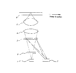
Referring now to Figure 1 of the drawings an
optical pickup device of this invention is shown which
comprises a light source such as a semiconductor laser 1,
an optical lens system, including a grating 2, a
collimating lens 4 and an object lens 5, to converge light
beams from the light source on a recording medium 6, a
photodetector 7 for detecting light beams reflected from
~-the recording medium 6, and a hologram optical~ element 3
for introducing the reflected light into the photodetector
7.
,,
. ~ ) ~, ,,, ~.
.
. , .
'" ' ' . .
,
.
`` 1 3 1 7674
A light beam from the semiconductor laser 1 is
diffracted by the grating 2, resulting in three separate
beams, one of which is the zero-order diffracted beam
(below referred to as the main beam), and the others of
which are first-order diffracted beams (below referred to
as the sub-beams) in the positive and negative directions
that are substantially orthogonal to the plane including
Figure 1. These three separate beams are further
diffracted by the hologram optical element 3. The
resulting zero-order diffracted beam of each of the above-
mentioned separate beams enters the object lens 5 via the
collimating lens 4 and is focused on a pit of the recording
medium 6. A pit signal (i.e., an information signal)
results from the int.ensity of the beam reflected from the
recording medium 6. The two sub-beams, which are
positioned symmetrically with respect to the above-
mentioned main beam, are focused on the recording medium 6
in such a way that they shift to a large extent in the
tracking direction and to a small extent in the radial
direction. A difference in the intensity between the two
sub-beams reflected from the recording medium 6 gives a
tracking error signal. The beams reflected from the
recording medium 6 pass through the object lens 5 and the
collimating lens 4 and are di~fracted by the hologram
optical element 3. The resulting first-order diffracted
beams are introduced into the photodetector 7. The
semiconductor laser 1 and the photodetector 7 are-fixed to
each other within the same package.
Figura 2(a) ~hows the relationship between the
configuration of a number of grating lines of the hologram
optical element 3 that ls seen from the recording medium 6
and Figure 2(b) shows the configuration of the
photodetector 7. Figure 2(c) shows the orientation of the
devices in Figures 2(a) and 2(b). The holog~am optical
element 3 is divided into two regions 3a and 3b by a
division line 3c in the radial direction. The regions 3a
.
.
---"` 1 3 1 7674
and 3b have a number of grating lines, the pitches of which
are different from each other. Each of the grating lines
is gently inclined to eliminate abberations. The
photodetector 7 is divided into five regions 7a, 7b, 7c,
7e, and 7f. The division line A~ is slightly inclined with
respect to the direction of the diffraction of the hologram
optical element 3 so as to prevent occurrence of a focus
offset. When the beam from the semiconductor laser 1 is
precisely focused on the recording medium 6 or at the
correct focus, the resulting main beam that has been
diffracted by the region 3a of the hologram optical element
3 is focused on the division line Ao of the photodetector
7 to form a spot Pl. The resulting main beam that has been
diffracted by the region 3b of the hologram optical element
3 is focused on the photodetecting region 7c to form a spot
P2. When output signals of the photodetecting regions 7a,
7b, 7c, 7e, and 7f are represented respectively as Sa, Sb,
Sc, Se, and Sf, a focus error signal is obtained by
calculating (Sa-Sb), a tracking error signal is obtained by
calculating (Se-Sf), and a pit signal is obtained by
calculating (Sa + Sb ~ Sc).
In the optical pickup device of the present
invention with the above-mentioned structure, the
adjustment of this device for the elimination of a focus
offset can be attained by shifting a spot Pl alone because
the spot P2 has no relation to a focus error signal.
Accordingly, by the rotation of the hologram optical
element 3, the spot Pl that is formed on the photodetector
7 is shifted in the direction of the x-axis , so that the
adjustment of this device for elimination of a focus offset
can be attained. In this way, because the forward or
~ backward movement of the hologram optical element 3 is
-~ unnecessary to eliminate such a focus offset, the size of
, the hologram optical element 3 can be set at that of the beams that enter the same hologram optical element 3.
'
.
,7
... . . . .
1 3 1 7674
Moreover, the effective photodetecting area of the
photodetecting region 7a is approximately equal to that of
the photodetecting region 7b, and the total of the two
effective photodetecting areas is approximately equal to
the effective photodetecting area of the photodetecting
region 7c. This is because the influence of light
reflected from the cap of the semiconductor laser 1 and/or
of dark current to the photodetector 7 on the signals with
respect to the region 7a becomes equal to that of the
region 7b, thereby suppressing occurrence of an offset in
error-detecting signals.
Figure 7 shows another optical pickup device of
this invention in which the hologram optical element 33 is
divided into two regions 33a and 33b by a division line 33c
in the radial direction. The regions 33a and 33b has a
number of grating lines that are symmetrical with respect
to the division line 33c. The photodetector 37 is divided
into five regions 37a, 37b, 37c, 37e, and 37f. The beams
that have been diffracted by the hologram optical element
33 are focused on the division line A3 of the photodetector
37 and on the photodetecting region 37c, respectively, to
form spots S1 and S2. When output signals of the
photodetecting regi~ns 37a, 37b, 37c, 37e, and 37f are
represented respectivelY as S3a/ S3bl S3CI S3e, and S3f ~ a
focus error signal is obtained by calculating (S3a-S3b), a
tracking error signal is obtained by calculating tS3~-S3f),
and a pit signal is obtained by calculating (S3a + S3b +
S3c)~ The focus offset phenomenon can be prevented by the
shifting of the spot Sl alone, which is performed by the
rotation of the hologram optical element 33. Thus, the
size of the hologram optical element 33 can be set, as
well, at that of the beams that are incident upon it.
Moreover, for the same reason as described in Example 1,
the effective photodetecting area of the photodetecting
region 37a is approximately equal to that of the
.
;~.
'I -. `';
1 3 1 767~
11
photodetecting region 37b, and the total of the two
effective photodetecting areas is approximately e~ual to
the effective photodetecting area of the photodetecting
region 37c.
Although the above-mentioned embodiments only
disclose an optical pickup device with a three-beam mode,
the invention is, of course, applicable to an optical
pickup device with a one-beam mode at the time when the
parts of the pickup device are positioned so that the
division line 3c(33c) of the hologram optical element 3(33)
is positioned in the tracking direction, thereby
representing a tracking error signal by [Sc - (Sa + Sb)] -
{ or [S3~ - (S3a + S3b)]
`,
..... ,.,,,,,,,,~ ~