Note : Les descriptions sont présentées dans la langue officielle dans laquelle elles ont été soumises.
1~21027
VECTOR TAILGATING IN COMPUTERS
WITH VECTOR REGISTERS
FIELD OF THE INVENTION
This invention pertains to the field of high
performance vector computers, and in particular to
apparatus and methods for controlling the use of vector
registers in a process referred to herein as "tailgating"
to provide performance gains in vector computations.
BACKGROUND OF THE PRIOR ART
In the field of large, very high performance
computers~ usually referred to as supercomputers, a vec-
tor processing architecture is usually provided in order
to achieve very high data processing rates in com-
putations involving ordered sets of data, or vectors. A
very successful supercomputer vector processing archi-
tecture is disclosed in U. S. Patent No. 4rl2~,880 by
Seymour R. Cray and assigned to Cray Research, Inc. In
that architecture, a plurality of vector registers are
provided to hold vectors for sending as operands to
functional units, and for receiving and holding result
vectors from functional units. For maximum speed, fully
segmented functional units are provide~ wherein all
information arriving at the functional unit or moving
within the functional unit is captured and held at the
end of every time period. Vector registers used as
operand registers for a given vector process transmit
individual elements to a functional unit at the rate of
one element per time period. Once the startup time, or
functional unit time, has passed, the functional unit
provides successive result elements on successive time
periods, and these are transmitted as elements of a
result vector to a vector register acting as the result
1321027
--2--
register for that particular vector process. Vector
transfers between vector registers and main memory may
also be accomplished at one element per time period.
By providing a number of functional units (for
example, floating point multiply, integer add, logical
operations, etc.) and a number of vector registers tfor
example, eight), any of which may be associated by
program instruction control with any functional unit or
memory, computers according to U. S. Patent No.
4,128,880 may have numerous vector processes proceeding
simultaneously, thereby achieving extremely high data
processing rates.
SUMMARY OF THE INVENTION
The present invention provides further im~rove-
ments in processing speed for vector register computers
of the type described above through a technique referred
to herein as tailgating. Briefly stated, tailgating
refers to a technique for more efficient utilization of
vector registers, wherein a vector may be written into a
v0ctor register simultaneously with the reading
therefrom of another vector which was previously stored
therein. The tailgating vector to be written into the
register can come from a functional unit or from common
memory. The technique uses reading and writing of one
vector element per time period, with the writing
occurring one or more elements behind the read operation
so as to not overwrite elements which have yet to be
read. By this technique a given vector register can be
used both as an operand register and a result register
for the same vector operation. In other words, a vector
register can be loaded with a vector, element by ele-
ment, while a previously loaded vector is still being
1321027
--3--
used and read from the vector register, element by ele-
ment. By this techni~ue, a vector instruction in a
program which calls for the use of a particular vector
register which is involved in a previously issued vector
instruction can issue immediately without having to wait
for a completion of the earlier vector instruction.
Upon the element-by-element read oE one vector, each
element of the vector register becomes available for an
element-by-element write of another vector.
DESCRIPTION OF THE DRAWINGS
In the drawings, where like numerals refer to
like elements throughout the several views,
Fig. 1 is a detailed block diagram of the com-
putation section of the computer incorporating the pre-
vent invention;
Fig. 2 is a timing diagram of the tailgating
instruction, V0 = V0 + V0, as executed in the first pre-
ferred embodiment;
Fig. 3 is a schematic block diagram of the
vector register control for the first preferred embodi-
ment;
Fig. 4 is a schematic block diagram of the
vector register memory for the first preferred embodi-
ment;
Fig. 5 is a timing diagram of a three instruc-
tion tailgating sequence as executed in the second pre-
ferred embodiment.
Figs. 6, 7, 8 and 9 combined form a timing
diagram further describing the events occurring during
the instruction sequence of Fig. 5;
Fig. 10 is a schematic block diagram of the
vector register memory for the second preferred embodi-
_4_ 132~27
ment;
Fig. 11 is a schematic block diagram of thevector register reservation control for the second pre-
ferred embodiment;
Fig. 12 is a schematic block diagram of the
tailgate slot time control for the second preferred
embodiment;
Fig. 13 is a schematic block diagram of the
vector address control for the second preferred embodi-
ment;
Fig. 14 is a schematic block diagram of the
vector address offset control for the second preferred
embodiment.
DETAILED DESCRIPTION OF THE
PREFERRED EMBODIMENT
In the following detailed description of the
preferred embodiments, reference is made to the accom-
panying drawings which form a part hereof, and in which
is shown by way of illustration two specific embodiments
in which the invention may be practiced. Both embodi-
ments are described in terms of block diagrams and
timing diagrams, upon which detailed logic designs (not
shown) could be based, as is generally known in the art.
It is to be understood that other embodiments may be
utilized and that structural changes may be made
without departing from the scope of the present inven-
tion.
The configuration and operation of the vector
processing and control means according to the present
invention can best be understood by beginning with a
general description of the organization of a computer
system employing the present invention. Details of the
1321027
--5--
configuration and operation of the invention will then
be presented.
In the block diagram of Fig. 1, the com-
putation section of a computer system is shown in
detail. The computation section includes a set of vec-
tor registers generally designated by reference number
100. The vector registers form the major computational
registers of the computer because they provide high
speed processing of data. In both preferred embodi-
ments, there are eight individual vector registers,
designated as V0 through V7 in Fig. 1. Each vector
register consists of 64 individual elements as indicated
by the octal designation of elements 00 through 77 on
vector register V0. Each element holds a 64 bit word.
Three functional units are dedicated to vector
processing. These are the integer unit 110, the logical
unit 120 and the shift unit 130. Two additional func-
tional units are shared between the vector and scalar
portions of the computer. These are the floating point
functional units for addition 140 and multiplication
150.
A vector operation begins by obtaining
operands from the first element of one or more vector
registers and delivering them to a functional unit.
Successive elements are provided in each time period
and as each operation is performed, the results are
delivered to successive elements of the destination vec-
tor register. The vector operation continues until the
number of operations performed by the instruction equals
the count specified by the contents of a Vector ~ength
register 160.
In symbolic representations of vector opera-
tions, including the drawings and specifications herein,
vector registers are identified by the subscripts i, j,
13~:l027
--6--
and k. Subscript i is used to identify the destLnation
vector register. Subscripts j and k are used to iden-
tify operand vector registers. For example,
Vi = vj + Vk
Elements of a vector register are identified with a
numeric subscript (e.g., V46 is element 6 of vector
register 4).
An element of a vector register may be
transmitted as an operand to a functional unit and then
provide the destination for a result from a previous
operation in a subsequent time period. The use of a
register as both an operand register and then a destina-
tion register allows for the "tailgating" of two or more
vector operations together~ In this mode, two or more
results may be produced per time period. The time
period for these vector operations is normally a single
system clock period.
Except for this tailgating mode, vector
registers are reserved for the period of time in which
they are involved in vector operations. Other instruc-
tions that require the same vector registers, but which
cannot execute in a tailgating mode, will not issue
until the previous instruction is completed and the
reservation is dropped. ~owever, since all functional
units are independent, multipl~ unrelated vector pro-
cessing operations can be underway simultaneously using
different functional units and different operand and
result vector registers.
1'~21~27
First Preferred Embodiment
The first preferred embodiment of the present
invention is illustrated by the drawings in Figs. 2, 3,
and 4.
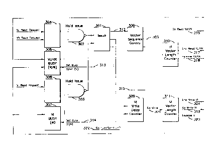
A schematic block diagram of the Vector
Register Control for the first preferred embodiment is
shown in Fig. 3. Circuit 301, labelled as Issue, has as
its input the complementary output rom AND gates 302
and 303. Both outputs are indicators that the instruc-
tion must wait before it can issue.
The input to AND gate 302 consists of the out-
put of circuit 305 and the signals Vj Read Request and
Vk Read Request held at latch 304. Circuit 305 examines
the Vj and Vk Read Busy and Write Busy bits. One Read
Busy bit and one Write Busy bit is provided for each
vector register. These bits indicate whether the
requested operand vector registers are currently busy
for a previous Read or Write operation. If the
requested operand vector registers are not busy, then
the complementary output from AND gate 302 allows the
instruction to issue.
The complementary output from AND gate 303
must be examined in conjunction with the complementary
output from AND gate 302 before the instruction issue
can occur. The input to AND gate 303 is the output from
circuit 307 and the signal Vi Write Request held at
latch 306. Circuit 307 examines the Vi Write Busy bit
to determine whether the requested destination vector
register is currently busy for a Write operation.
Instruction issue requires that the destination vector
register not be busy as a destination for a previous
instruction.
When instruction issue does occur, circuit 301
transmits signals on 313 to set Vj Read Busy and Vk
,
-8- i32~02~
Read Busy, and on 314 to ~et Vi Write ~usy. A signal 312
is also transmitted from circuit 301 to the Vector
Sequence Control 308. Vector Sequence Control 308, in
turn, generates Go Read Vj and Go Read Vk signals 316.
These signals act as input to the Vj/Vk Read Address
Counter 401 as indicated in Fig. 4. Signal 316 consists
of 8 bits--one for each vector register. Signal 316
indicates which of the vector registers is to be used
for the Read operations. Typically Vj would be dif-
ferent from Vk during the Read operation. However,
since Vj ma~y be the same vector register as Vk in this
embodiment, Go Read Vj and Go Read Vk may be the same
signal.
Vector Sequence Control 308 also transmits
signal 323 to trigger the Vj/Vk Vector Length Counters
represented in Fig. 3 by reference numeral 310.
Signal 323 consists of 8 bits--one for each Vector
Length Counter 310 associated with a vector register.
Typically Vj would be different from Vk during the vec-
tor read operation. However, since Vj may be the same
vector register as Vk in this embodiment, the Vj Vector
Length Counter and Vk Vector Length Counter may be the
same device.
The Vj/Vk Vector Length Counter 310 is ini-
tialized by a processor instruction, Load Vector Length,
which is issued by the application software. When Vj/Vk
Vector Length Counter 310 decrements to 0, it transmits
an End Read Vj/Vk signal 317 that clears Vj/Vk Read
Addres~ Counter 401 in Fig. 4. The Vj/Vk Vector Length
Counter 310 also transmits a Release Vj/Vk signal 318 to
clear the corresponding Read Busy bit.
Vector Sequence Control 308 also transmits
signal 315 to activate the Vi Write Delay Counter 309.
Signal 315 consists of 8 bits--one for each Write Delay
1321~27
_9_
Counter 309 associated with a vector register. The Go
Functional Unit signal 322 received by the Vi Write
Delay Counter 309 indicates the functional unit being
used and the amount of delay required before writing to
the destination vector register. The intelligence for
determining what functional unit delays are required is
contained in the Vi Write Delay Counter 309.
When the Vi Write Delay Counter 309 decrements
to 0, it transmits a signal Go Write 321 that triggers
the Vi Vector Length Counter 311. The Vi Vector Length
Counter 311 transmits a Go Write Vi signal 319 that is
input to the Vi Write Address Counter 402 and Vi Write
Enable latch 403 in Fig. 4.
The Vi Vector Length Counter 311 is ini-
tialized by a processor instruction, Load Vector
Length, which is issued by the application software.
The Release Vi signal 320 and End Write Vi signal 324
are transmitted by Vi Vector Length Counter 311 when
the counter decrements to 0. The Release Vi signal 320
clears the Vi Write Busy bit. Thereafter, another
instruction could issue using that vector register. The
End Write Vi signal 324 clears Vi Write Address Counter
402 in Fig. 4.
A schematic block diagram of the Vector
Register Memory for the first preferred embodiment is
shown in Fig. 4. The Vector Register 404 contains 3
inputs: a 6-bit Read Address 406, a 6-bit Write Address
407 and a Write 0/1 signal 408. The Vector Register 404
is unique in that the typical memory device has but 1
address input. This device has 2 distinct address
inputs, 1 for Read and 1 for Write. Each register chip
is 64 x 4 bits. Sixteen such chips make up a vector
register of 64 elements each element containing 64 bits.
The Vj/Vk Read Address Counter 401 increments
1321~27
--10--
by 1 upon receipt of the Go Read V~/Vk signal 316 and
continues incrementing every time period until it
receives the End Read Vj!Vk signal 317. The Vi Write
Address Counter 402 increments by 1 at every time period
where there is an active Go Write Vi signal 319.
The Go Write Vi signal 319 is also merged with
the Result Data 410 at Vi Write Enable 403. This merger
creates a Write 0/1 signal 408. This signal 408 is not
just a write strobe, but also provides the full ~4 bit
word which the Vector Register 404 is told to store.
The Read Data 409 from the Vector Register 404
must go to a Functional Unit 405 before it comes back to
be written. Therefore, the Read Address 406 is always
ahead of the Write Address 407. As long as the Read
Address ~ounter 401 is at least 1 greater than the Write
Address Counter 402, the circuit can operate in a
tailgating mode.
Fig. 2, which is a timing dia~ram of the
instruction, V0 = V0 + V0, will help clarify the concept
of tailgating. Gradations along the horizontal axes
represent the time unit. The upper half of the diagram
represents the control sequence for the operand vector
register. The lower half of the diagram represents the
control sequence for the destination vector register.
To execute the Add instruction, the operand
vector registers must be read and their contents
transmitted to the functional unit for processing. In
time period tO, a V0 Read Request is signalled. This
cignal is generated by the instruction decoder before
the instruction is issued.
In conjunction with the V0 Read Request
signal, two status bits for the desired vector must be
examined: a Read Busy bit and a Write Busy bit. When
V0 Read Busy and V0 Write Busy indicate that vector
register V0 is not being used as an operand nor as a
'
1321027
destination, the signal Issue VO Read is transmitted
back to the instruction decoder to allow the instruction
to proceed.
To allow vector register VO to be used as an
operand, it must not already be busy either on a Read or
Write operation. If another vector register is being
used as an operand, the control sequence would look like
the upper half of the diagram. However, the diagram is
complete for the sequence VO = VO + VO.
In time period tO, a VO Write Request is also
signalled. Vector register VO provides the destination
for the results of the Add instruction. All that need
be checked, via the Write Busy bit, is that the vector
register is not already a destination for a previous
instruction. A signal Issue VO Write is then trans-
mitted back to the instruction issue control.
In time period t3, instruction issue causes VO
Vector Sequence Control ~labeled in the timing diagram
as VO Control) to transmit a signal called Co Read VO
and set ~0 Read Busy. VO Read Address Counter (labeled
in the timing diagram as VO Read Address) has already
been initialized for element 0. The Go Read VO signal
causes VO Read Address Counter to increment at time
period t4. Therefore, element O is read from the vector
register and time period t5 will present the address for
element 1. This read and increment operation con-
tinues through subsequent time periods until all ele-
ments have been read. After all 64 elements have been
read at time period t67, VO Vector Sequence Control will
clear VO Read Busy. An End Read VO signal is trans-
mitted during the same period to VO Read Address Counter
that resets the element address to 0.
The operands are transmitted to the functional
unit. After some period of time, the resulting data is
i321~27
-12-
transmitted back to the V0 vector register, its destina-
tion Theoretically, an element which is read from a
vector register could be written with new data in the
subsequent time period.
Referring to the lower half of Fig. 2, in time
period t3 V0 write Addres~ Counter (labeled in the
timing diagram as V0 Write Address) contains element
address 0. Instruction issue causes V0 Write Busy to
set and V0 Vector Sequence Control transmits a Go Write
V0 signal. V0 Write Address Counter remains at element
0 for 2 time periods t3 and t4. As soon as V0 Read
Address Counter is 1 and V0 Write Address Counter is 0
(time period t5), element 0 is written with new data.
Therefore, there is a 1 time period difference between
the Read and the Write operation. Normally, there would
be functional unit time between the Read and the Write
operations.
Functional unit delay time guarantees that
an element being read from will not be written to in the
same time period. In Fig. 2, the V0 Write Address
Counter is shown being held at element address 0 for 2
time periods. In actuality, Vi Write Address Counter
would be held at element address 0 for the number of
time periods indicated by Vi Write Delay Counter 309 in
Fig. 3.
Once the Write operation begins in time period
t5, V0 Write Address Counter advances at every time
period in a fashion similar to the V0 Read Address
Counter. As each element comes into the destination
vector register, it is written into the currently
addressed element, which is always at least 1 count
behind the address being read. V0 Write Address Counter
increments through all 64 elements until time period
t68, at which point V0 Vector Sequence Control clears
1321~27
-13-
V0 Write Busy and transmits an End Write V0 signal to V0
Write Address Counter that resets the element address
to 0.
In this embodiment, common memory can be
treated as a functional unit for tailgating purposes. A
vector being transmitted from common memory to a vector
register can tailgate a vector being used in a previous
instruction Instead of timing the tailgating operation
based on functional unit time, the memory transfer time
is used.
Second Preferred Embodiment
The second preferred embodiment of th~ present
invention is illustrated by the drawings in Figs. 5, 6,
7, 8, 9, 10, 11, 12, 13 and 14.
A Vector Register in the second preferred
embodiment is separated into 4 banks. As illustrated in
Fig. 10, the banks are labeled Bank 0, Bank 1, Bank 2,
Bank 3. Each bank gets every fourth element as labeled
in Fig. 10: Bank 0 contains element 0, element 4, ele-
ment 8, etc.
The register chips are a fast 16 x 4 memory.
The cycle time for the register chips is 2 time periods.
Each bank of the register is accessed every 4 time
periods. Therefore, when not operating in a tailgating
mode, a bank is active for 2 time periods and idle for
2 time periods. The sequence 2 time periods active, 2
time periods idle is repeated indefinitely.
Each bank has its own address register,
labeled in Fig. 10 as the Chip Address 1001 through
1004. The Element Address Counter 1005 is a 6-bit
address counter. During register access it counts
se~uentially, incrementing every time period. The
1321027
-14-
least significant 2 bits of the address are the Bank
Select bits 1006. The most significant 4 bits are the
Chip Address bits 1007. Chip Address 1008 is simply a
register whereby the most significant 4 bits are fanned
out to the difEerent banks. The Bank Select Decoder
1009 selects which bank is to be accessed by the Chip
Address signals 1020.
In order to do tailgating, to generate the
Write Address for the tailgating instruction, the bottom
path labeled Vector Address Offset 1010 is used. The
Vector Address Offset 1010 is 4 bits. The Vector
Address Offset 1010 is sent to the register 1011 at
issue time. Register 1011 is fanned out to register
1012 for each vector register via AND gate 1027.
Tailgate V0 signal 1025 is also sent at issue time.
Once the Tailgate V0 signal 1025 becomes active, the
Vector Address Offset is held in the Vector Address
Offset Register 1012 associated with the selected vector
register via AND gate 1028.
In order to generate the address for the
tailgating instruction, the 4-bit output from Chip
Address 1008 is run through a Subtractor 1013 to
subtract off the Vector Address Offset held at register
1012. The output of the Subtractor 1013 is called the
Adjusted Address 1019 and is routed back to Chip Address
1001. This offset relates to the functional unit delay
time and the amount of time elapsed between issuing the
two instructions involved in the tailgating operation.
Since the bank cycle time is 4 time periods,
the element 0 address is stored in Chip Address 1001
during the first 2 time periods. The Ad]usted Address
1019 is stored in Chip Address 1001 the last 2 time
periods. The subtract need only be executed once for
each group of 4 elements. To access subsequent banks
1321027
-15-
the initial Adjusted Address 1019 is transmitted to the
next bank's Chip Address. Since an element is written
on every time period, a Subtractor is not needed for
every bank. The Chip Address is going to be the same
for the first four references, then it is incremented by
l for the next four addresses. The ~ank Select bits
1006 provided by the Element Address Counter 1005 deter-
mine which bank is selected. One of the necessary con-
ditions for tailgating in the second preferred
embodiment is that the vector register be supplied
results every single time period in sequence.
Operations which do not supply a result every time
period in sequence are not allowed to tailgate.
In this embodiment, tailgating is a multi-
plexing operation. Every two time periods a new address
is put into Chip Address 1001 through 1004, first a Read
Address, then a Write Address. If the operation is
not a tailgating operation, then the sequence is: Read
or Write Address for two time periods; "don't care" for
two time periods; Read or Wxite Address for two time
periods; etc.
In contrast to the first preferred embodiment,
the second preferred embodiment does not contain
separate reservation bits for each vector during Read
Busy and Write Busy. Instead reservation should be
thought of in terms of which one of the two possible
bank cycles is being used. There is a reservation flag
for the first bank cycle and another reservation flag
for the second bank cycle.
Fig. 11 shows the Vector Register Reservation
circuitry for a single vector register. Three busy
flags or reservation flags, labeled as 1101, 1102 and
1103, are shown in the diagram. As mentioned earlier,
the cycle time for each vector register bank is two time
i32tO27
-16-
periods ~nd the bank i9 accessed every four time
periods. During a tailgating operation, the first cycle
is a Read and the second cycle is a Write.
Latch 1101, also labeled as V0 Busy-l, is used
to indicate that the first two time periods, of a four
time period cycle, are reserved. Latch 1103, labeled as
V0 Busy-2, is used to reserve the second two time
periods. This latch only sets when the vector register
is operating in a tailgating mode. Latch 1102,
labeled as V0 Busy-3, is a composite use~ for timing
purposes.
V0 Busy-l 1101 sets on a request for the vec-
tor register at instruction issue time (assuming V0
Busy-l 1101 is not already set). V0 Busy-2 1103 sets on
a request of the vector register at instruction issue
time when V0 Busy-l 1101 is already set. V0 Busy-3 1102
is held as long as V0 Busy-l 1101 is set, except when
slot time occurs, then V0 Busy-3 clears for one time
period. Once V0 Busy-2 1103 is set, it remains set
until a ~elease V0 signal 1104 is received from Vector
Address Control. During tailgating, two Release V0
signals 1104 are used. The second release signal will
clear V0 Busy-2 1103 while the first clears V0 Busy-l
1101. With both V0 Busy-2 1101 and V0 Busy-2 1103
cleared, V0 Busy-3 1102 will clear as well.
V0 Busy-l is set at 1108 by the ORed outputs
of AND gates 1107 and 1109. AND gate 1107 will hold the
contents of V0 Busy-l until a complement of Release V0
signal 1104 causes it to clear. AND gate 1109 will
cause V0 Busy-l 1101 to set at instruction issue time
1106 when Request V0 1105 is signalled and V0 Busy-l
1101 is not in use.
V0 Busy-3 is set at 1111 by the ORed outputs
of AND gates 1110, 1112, and 1113. AND gate 1110 has as
132lo27
its input the output erom V0 ~usy-l 1101 and the comple-
ment of the signal V0 Slot Time 1208. AND gate 1112
will set V0 Busy-3 1102 at instruction issue time 1106
when Request V0 1105 is signalled. AND gate 1113 will
hold V0 Busy-3 1102 set when V0 Busy-2 1103 is set and
either V0 Busy-1 1101 is set or Release V0 1104 is not
signalled.
V0 Busy~2 1103 is set at 1115 by the ORed out-
put from AND gates 1116 and 1113. AND gate 1116 will
set V0 Busy-2 1103 at instruction issue time 1106 when
V0 Busy-l 1101 is set and Request V0 1105 is signalled.
AND gate 1113 holds V0 8usy-2 1103 set when the output
from OR gate 1114 is 1. OR gate 1114 has as its input
V0 Busy-l 1101 and the complement of the Release V0
signal 1104.
Fig. 12 is a schematic diagram describing the
Tailgate Slot Time circuitry. Depending on the func-
tional unit time of the tailgating instruction, the
instruction must be issued at a time that will sychro-
nize the Write operation with the Read operation
currently in progress against the vector register. Four
different slots are used to perform the synchronization
function using latches 1201, 1202, 1203, and 1204 in
Fig. 12. Each slot corresponds to one of four different
time periods in a memory cycle.
Two time periods after the first instruction
issues, the slot counter, implemented by latches 1201,
1202, 1203, and 1204, begins counting at Slot 2.
Latches 1205 and 1206 insure that the succeeding
instruction does not issue too soon; a two time period
delay is added to the second instruction when tail-
gating.
The slot counter is set by the output from AND
gate 1215. This AND gate 1215 has as its input the com-
~32l~27
-18-
bination of signals: Request V0 1105; the complement of
V0 Write Request 1317; the complement of Request Memory
1207; the complement of V0 Busy-l 1101; and Issue 1106.
The signal Request V0 1105 causes the slot counter to
start only when the vector register is initiall~
requested. By using the complement of the signal V0
Write Request 1317, the slot counter is started only if
the vector register request is for a Read operation.
The complement of the signal Request Memory 1207 pre-
vents tailgating during a common memory operation, a
restriction only in the second preferred embodiment.
The complement of the signal V0 Busy-l 1101 prevents the
slot counter from being re-initialized while it is
operating. The signal Issue 1106 allows the slot
counter to initialize only at instruction issue time.
After the first instruction has issued,
assume the tailgating instruction is in position to be
decoded and issued. The tailgating instruction need not
be executed immediately after the first instruction;
several non-related instructions could be executed bet-
ween the first instruction and the tailgating instruc-
tion. Depending on the instruction type, one of four
"request slot" signals (e.g., Request V0 Slot 0 1216) is
transmitted by the instruction decoder. For example, a
Vector Logical Product instruction requests slot 0.
Therefore, in the decode process a Request V0 Slot 0
signal 1216 is transmitted. A different functional
unit operation could result in a different slot request
to synchronize the Write operations.
Since the signal generated by V0 Busy-3 1102
in Fig. 11 is preventing instruction issue, this signal
must be interrupted for one time period for the
tailgating instruction to issue. As shown in the bottom
half of Fig. 12, the signal Request V0 Slot 0 1216 is
~ 321 027
--19--
ANDed at 1209 with the signal generated by latch 1201,
labeled V0 Slot 0, to generate a signal labeled V0 Slot
Time 1208. In a similar fashion requests for other
slots are ANDed with the output from the corresponding
latches 1201, 1202, 1203, or 1204. Any of the resulting
signals can set V0 Slot Time 1208 via OR gate 1214.
This V0 Slot Time signal 1208 acts as input to
the Vector Register Reservation circuitry in Fig. 11.
The complement of the signal V0 Slot Time 1208 is ANDed
with the output from V0 Busy-l 1101 at 1110 and then the
result is ORed as input to V0 Busy-3 1102 at 1111. The
signal transmitted by V0 Busy-3 1102, as indicated
above, holds instruction issue. The complementary
signal V0 Slot Time 1208 clears V0 Busy-3 1102 for one
time period, thereby allowing instruction issue provided
there are no other conflicts.
When the tailgating instruction issues, V0
Busy-2 1103 is set through an AND operation at 1116 on
the signal Issue 1106 and the output from V0 Busy-l
1101. V0 Busy-2 1103 prevents a subsequent tailgating
operation from occurring for the same vector register.
The contents of V0 Busy-2 1103 are ANDed with the con-
tents of V0 Busy-l 1101 to provide input to V0 Busy~3
1102, thereby preventing V0 Busy-3 1102 from clearing at
the next V0 Slot Time signal 1208.
Referring now to Fig. 13, the Vector Address
Control circuit contains an Element Address Counter
1005, a Variable Delay 1304, a Normal Vector Length
Counter 1302, and a Tailgate Vector Length Counter
1301.
The Variable Delay 1304 is triggered by the
Write VO signal 1317 generated at instruction issue
time. The amount of delay is determined by the Go
Functional Unit signal 1315 which indicates which func-
~ 321027
-20-
tional unit is used and the Tailgate signal 1330.
Different delay values are used for normal vs.
tailgating instructions. Upon delaying the proper
amount of time, the Variable Delay 1304 transmits a
signal Begin Write 1318. The Begin Write signal 1318
sets latch 1328 which in turn transmits the Write Mode
signal to the vector register. The Write Mode signal
from latch 1328 indicates that the transmitted element
address is for a write operation.
The Begin Write signal 1318 is ORed at 1309
with the signal Go Read V0 1319 issued by the instruc-
tion decoder. The output from OR gate 1309 sets latch
1305. Thus, latch 1305 sets immediately after issue for
a Read operation or after a predetermined delay for a
normal Write operation. The output from latch 1305
enables the operation of the Normal Vector Length
Counter 1302. When the Normal Vector Length Counter
1302 holds a value of 1, it resets latch 1305, thereby
disabling the Normal Vector Length Counter 1302. The
normal Vector Length Counter 1302 will have decremented
to 0 by the time the enable is dropped.
During a tailgating operation, the Begin
Write signal 1318 is ANDed with the Tailgate signal 1330
at 1314. The output from AND gate 1314 sets latch 1306.
The output from latch 1306 enables the operation of the
Tailgate Vector Length Counter 1301. When the Tailgate
Vector Length Counter 1301 holds a value of 1, it resets
latch 1306, thereby disabling the Tailgate Vector Length
Counter 1301. The Tailgate Vector Length Counter 1301
will have decremented to 0 by the time the enable is
dropped.
Both the Normal Vector Length Counter 1302 and
the Tailgate Vector Length Counter 1301 transmit the
Release V0 signal 1104, via OR gate 1312, when either
~ 321~'~7
-21-
counter reaches the value of 1. Both counters decrement
at every time period as indicated by the inputs 1322 and
1323. Circuit 1324 generates an extra Release V0 signal
1104 if both counters decrement to 1 simultaneously.
The Tailgate Vector Length Counter 1301 is
used strictly for tailgating operations. It performs
basically the same function as the Normal Vector Length
Counter 1302. Note that for the Normal Vector Length
Counter 1302, a complement Tailgate signal 1330 loads
the counter with the Vector Length Data 1326 at AND gate
1310. In contrast, a Tailgate signal 1330 loads the
Tailgate Vector Length Counter 1301 with the Vector
Length Data 1326 at AND gate 1313. The Go V0 1325
signal indicates instruction issue at both AND gates
1310 and 1313.
Either Vector Length Counter 1301 or 1302
enables the Element Address Counter 1005 as long as both
counts are not 0. The output from the Normal Vector
Length Counter 1302 is ANDed with the output from latch
1305 at 1329. The output from Tailgate Vector Length
Counter 1301 is ANDed with the output from latch 1306 at
1311. The output from AND gates 1329 and 1311 provide
the input to OR gate 1307 which in turn provides the
enable signal to both Element Address Counter 1005 and
the Step V0 latch 1308. The output from Step V0 1308
indicates to the Vector Register Memory that the Element
Address Counter 1005 value is valid.
The Normal Vector Length Counter 1302
transmits the Inhibit Tailgate signal 1321 to the
instruction issue control whenever the count is less
than the value 7. Signal 1321 is used to prevent
problems with issue control. If the read count gets too
small, signal 1321 inhibits the initiation of a
tailgating instruction. If a tailgating instruction is
132102~
-22-
in progress at the time, it is not affected by signal
1321.
The Element Address Counter 1005 increments on
each time period as indicated by input 1327. The
Element Address Counter 1005 is cleared by the Release
V0 signal 1104. When tailgating, the first Release V0
signal 1104 is ignored by the Element Address Counter
1005.
The enable signal 1307 from the Tailgate
Vector ~ength Counter 1301 can cause the Element Address
Counter 1005 to count beyond the length used for the
first instruction. This allows the tailgating instruc-
tion to write data to the vector register by subtracting
the Address Offset from the Element Address Counter 1005
value.
Fig. 14 illustrates the Vector Address Offset
circuitry. The 4-bit register V0 Address Offset 1409 is
set by OR gate 1419. OR gate 1419 has as its input the
output from AND gates 1418, 1420, and 1421. AND gate
1421 initializes the V0 Address Offset register 1409 at
instruction issue time. The input to AND gate 1421 is
the value 2 which is gated by the output from AND gate
1422. AND gate 1422 has as its input the signals
Request V0 1105, Issue 1106, and the complement of V0
Busy-l 1101. Thus, V0 Address Offset 1409 is ini-
tialized with the value 2 when a request is made of
Vector Register V0, at instruction issue time, and so
long as V0 is not already busy.
The contents of V0 Address Offset 1409 are
held by the output of AND gate 1420. The other two
inputs to AND gate 1420 are the signals V0 Busy-l 1101
and the complement of V0 Slot 1 1202. Therefore, the
"wrap around" of V0 Address Offset 1409 occurs while the
vector register V0 remains busy and the V0 slot
13210~7
-23-
counter does not indicate slot 1.
The value held in V0 Address Offset 1409 is
incremented whenever the V0 slot counter indicates slot
1. The AND gate 1418 has as its input the signal V0
Slot 1 1202 and the value from V0 Address Offset 1409
incremented by 1 by the adder 1408.
The Address Offsets for all vector registers
are fanned into a single selection network 1401. The
desired Address Offset i9 chosen by the i-designator
signal 1417 identifying the destination vector register.
The Address Offset is transmitted and held at re~ister
1407. Only one Address Offset need be selected at 1401
because the Vector Address Offset 1010 is only sent at
instruction issue time. Subsequently, the value held at
Vector Address Offset 1011 is fanned out to all eight
vector registers as shown in Fig. 10. The Vector
Address Offset Register 1012 (one of eight) is loaded at
instruction issue time only if the corresponding
Tailgate signal 1025 (one of eight) is present.
The output from register 1407 is de~ivered to
four adders 1402, 1403, 1404, and 1405. The output from
these adders provide the input to the selection network
1406. At instruction issue time one of four signals
indicates which of the adder outputs to select. These
signals are labelled in Fig. 14 as Adjusted Offset +3
1423, Adjusted Offset +2 1424, Adjusted Offset +1 1425,
and Adjusted Offset +0 1426. Only one signal is active
at any time. The signals are then held in a set of
latches 1415 and will control the selection network 1406
via the signal 1416.
The resulting Vector Address Offset 1010, also
shown in Fig. 10, is a number that must be subtracted
from the Chip Address 1020 to arrive at the Adjusted
Address 1019 for the tailgating operation. What is
132~2~ .
-24-
measured by the Adjusted Address 1019 is the amount of
time between the issuance of the first instruction and
the issuance of the tailgating instruction plus the
functional unit delay time of the tailgating instruc-
tion. There could be any number of instructions issued
in between. As shown in Fig. 14, when the first
instruction issues, the Vector Address 1409 is ini-
tialized with the value 2 and incremented every ~ time
periods by the ~lot l signal 1202. Eventually the
tailgating instruction is issued. At instruction issue
time for the tailgating instruction, the Address
Offset 1409 is adjusted by the values 0, l, 2, or 3~
This final adjustment depends on the functional unit
time of the tailgating instruction.
The timing diagrams of Figs. 5, 6, 7, 8, and 9
will help explain the tailgating invention as imple-
mented in the second preferred embodiment.
Fig. 5 is a timing diagram illustrating a
typical tailgating operation. The diagram shows the
second instruction (V0=V3 & V4) tailgating the first
instruction (V2=V0+Vl), and the third instruction
(V3=V5>Ak) tailgating the second instruction. In the
timing diagram of Fig. 5, the gradations along the hori-
zontal axes represent time periods. The horizontal
lines, broken into 3 segments (dashed, solid, dashed)
represent the amount of time required to deliver an
operand to a functional unit, the number of time periods
required by the functional unit, and the number of
time periods required to deliver a result to a destina-
tion vector respectively. Delivery times may change
depending upon whether the functional unit resides on
the same module as the vector registers. Such is the
case in the second instruction using the Logical func-
tional unit.
-25- 1 321~27
At time period t4 in Fig. 5 the vector
registers VO and Vl begin supplying operands to the
Integer functional unit. The subsequent lines of Fig. 5
show the cycle through the subsequent elements and
instructions. The operands are supplied at a rate of
one element per time period.
The results start coming back from the second
instruction, the VO tailgating instruction, at time
period tl4. Therefore, vector register VO must be ready
for a write operation at time period tl4. The first
result, element 0, is written during the periods
following the read of element 8 for the first instruc-
tion. After element 9 is read, element 1 is writt~n.
After element 10 is read, element 2 is written. This
describes the basic flow of data to and from the vector
register VO during a tailgating operation.
Instruction issue control must examine the
tailgating instruction and determine, knowing the amount
of delay that a functional unit will cause, which time
period the first result will return to be stored in
the vector register at element 0. Based on this infor-
mation, vector register control delays the second
instruction until it is in synchronization with the bank
cycle of the vector register.
In the second preferred embodiment, the com-
puter, at its fastest, can issue an instruction once
every two time periods. In the event of a tailgating
instruction, the earliest that the second instruction
can issue is time period t5. In the example of Fig. 5,
the second instruction is he~d for one additional ti~e
period to make sure it is in synchronization with the
bank cycle. This insures that the reading and the
writing of vector register elements occur in the correct
sequence. Fig. 5 can be described in terms of holding
1321~27
-26-
instruction issue to synchronize for tailgating.
Without tailgating there would be a register con~lict
which would cause the second instruction to hold issue
until all result elements of the fir~t instruction were
stored.
In Fig~ 6, the instruction issue timing
diagram, at time t0 the Add instruction is issued. The
Add instruction sets V0 Busy-l and V0 Busy-3. Both
remain set for the duration of the Add operation, except
when V0 Busy-3 clears for a single time period to allow
the tailgating instruction to issue. The third line
indicates the Tailgate Slot Time operation. Two initial
delays occur, then the V0 slot counter begins operating
as a ring counter. The fourth line shows the V0 Address
Offset. It is always initialized with a value o~ 2,
then ever~ time V0 slot 1 is indicated by the V0 slot
counter, the V0 Offset is incremented by 1. The fifth
line shows the signal Request V0 Slot 3. The Request
V0 Slot 3 signal is generated by the tailgating instruc-
tion waiting to be issued. The signal Go Read V0 is
generated by the Add instruction and triggers the
Element Address Counter (labeled in the timing diagram
as V0 Element Address) to read each element in vector
register V0. The last line assumes a vector length of
100 (octal) in the Normal Vector Length Counter (labeled
in the timing diagram as V0 Length Counter) that decre-
ments as each element is read from the vector register.
At time period t4, V0 Slot 3 is indicated and
the signal Request V0 Slot 3 is active. The AND of
these two signals causes V0 Busy-3 to clear for a single
time period which allows the tailgating instruction to
issue provided all other is8ue conditions are met.
Issue of this instruction sets V0 Busy-2, Write VQ, and
initializes the Tailgate Vector Length Counter (labeled
1321~2~
in the timing diagram as V0 T.G. Length Counter) in time
period t7. The indication V0 of Slot 0 in time period t5
sets V0 Busy-3 once again and increments the V0 Address
~ffset by 1 count. Once the second instruction has
issued, the adjusted V0 Address Offset is transmitted to
the vector registers. The adjustment occurs in the same
time period as instruction is~ue. Thus, the V0 Address
Offset used for the Adjusted Address is the V0 Address
Offset from the previous time period containing the
value 2. From this point on the slot counter and the V0
Address Offset are not important.
Referring now to Fig. 7, by time period t4 the
Element Address Counter is at element address 2. In the
same time period the Normal Vector Length Counter has
decremented to the value 75 (octal). The upper four
lines of the diagram illustrate the vector register
memory operations occurring in each of the four vector
register banks. During the first two time periods data
is read from a vector register bank. During the next
two time periods the bank is either idle or writing new
data as the tailgating operation occurs. Time periods
t8, t9 and tlO show that the Tailgate Vector Length
Counter is held for 3 time periods before it begins to
decrement. The box at time period t9, also shown in
Fig. 7, is the V0 Address Offset. Because of propaga-
tion and fanout delays there is a period of time between
the actual issuing of the adjusted offset until it is
latched and held.
Referring now to Fig. 8, at time period tl4,
the first Write operation begins. The Subtract shown in
time period tl3 indicates a valid subtraction, at other
times the subtraction is occurring, it is just not used.
The V0 Address Offset is subtracted from the V0 Chip
Address every 4 time periods to provide the correct V0
1321~7
-28-
Chip Address for the subsequent Write operation. From
time period tl4 onward, the vector register banks are
reading and writing in the same time periods, thereby
illustrating the invention of tailgating. Although in
this example the Read operation terminates before the
Write operation, the vector lengths for the Read and the
Write are completely separate so the Write operation
could terminate before the Read operation.
Referring now to Fig. 9, the vector register
reservations are held until the last of the 2 operations
is completed. Both length counters independently decre-
ment to 0 and then transmit a Release V0 signal. The
first Release signal, in this example generated by the
Read operation, clears V0 Busy-l. The second Release
V0 signal, in this example generated by the Write opera
tion, clears V0 Busy-2 and V0 Busy-3.
The tailgating techniques disclosed herein
pro~ide significant improvements in processing speed for
the types of calculations encountered in typical appli-
cations. Although tailgating is independent of the
chaining technique disclosed in the previously mentioned
U. S. Patent No. 4,128,880, if desired, and if logic
space permits, tailgating may be used in conjunction
with chaining for further improvements in performance.
Although two specific configurations of com-
puter hardware have been illustrated and described for
the preferred embodiments of the present invention set
forth herein, it will be appreciated by those of ordi-
nary skill in the art that any arrangement of computer
hardware which is calculated to achieve the same purpose
may be substituted for the specific configurations
shown. Thus, the present invention disclosed herein may
be implemented through the use of different components
than those disclosed in the Detailed Description. This
1321027
-29-
application is intended to cover any adaptations or
variations of the present invention. Therefore, it is
manifestly intended that this invention be limited only
by the claims and the equivalents thereof.