Note : Les descriptions sont présentées dans la langue officielle dans laquelle elles ont été soumises.
~ 321~2g
COMPUTER LOOK~AHEAD INSTRUCTION ISSUE CONTROL
_eld of the Intention
This inventlon relates generally to control
logic for computer systems. In particular, it is
directed to look ahead control logic for instruction
issue.
Back~round of the Invention
To maximize computer performance, systems
designers have long sought techniques that minimize the
tims re~uired for instruction execution. Performance
gains are promoted by hardware architectures that include
a plurality of function~l units, vector registers, scalar
registers, address registers, and instruction buffers.
In order to justify the cost of these expensive
components, they must be kept reasonably busy. Parallel
instruction execution represents an effort to increase
the utilization of resources within a single processor.
In some computers, the instruction issue
process involves checking the reservation flags for the
resources involved in the operation during the clock
period when the instruction is scheduled to issue. The
instruction waits in the issue position until all of the
required resources are available. Immediately upon
instruction i~sue the reservation or busy flags are set
for the assigned resources by the instruction issue
control. Thereafter, subsequent instructions test these
reservation flags immediately prior to issue and hold at
the issue position if a resource conflict occurs.
In most computers, instruction issue occurs at
every clock period if there is no resource conflict.
Typically, the clock speed is slow enough that all
necessary conflict checks, followed by instruction issue,
can occur within one clock period. As clock speeds
increase, however, there is not enough time in one clock
period to resolve all the conflicts and then issue the
instruction.
1321029
one such computer is the Cray 2-supercomputer
built by Cray Research, Inc., the Assignee of the present
invention. Because of propagation and fan-out delays
caused by a four nanosecond system clock, the Cray 2
requires two clock periods to complete the "test and
issue" sequence of testing for resource conflicts and
then issuing the instruction. Therefore, the maximum
instruction issue rate of the Cray 2 i5 one instruction
every two clock periods.
Summary of the Invention
To overcome the limitations in the prior art
discussed above and to overcome other limitations readily
recognizable to those skilled in the art, the present
invention provides a new architecture for instruction
issue control.
According to one object of the present inven-
tion, the looX-ahead instruction issue control tests for
resource conflicts before ~he instruction issues. Rather
than check for resource conflicts only at instruction
issue time, the present invention performs this operation
for a plurality of pre-issue instructions.
Yet another object of the present invention is
to check for resource conflicts between each of the pre-
issue instructions and resources currently in use and for
conflicts with resources to be used by instructions ahead
of it in the instruction issue process.
Description of the Drawinqs
In the drawings, where like numerals refer
to like elements throughout the several views,
Fig. 1 is a combination hardware-and-timing
diagram of the register busy conflict checks, as executed
in the preferred embodiment;
Fig. 2 is a combination hardware-and-timing
diagram of the address and scalar register path conflict
Trademark
132~29
-3
checks, as executed in the preferred embodiment;
Fig. 3 is a combination hardware-and-timing
diagram of the functional unit conflict checks, as exe-
cuted in the preferred embodiment;
Fig. 4 is a timing diagram describing the
sequence for conflict checks, as executed in the pre-
ferred embodiment;
Fig. 5 is a combination hardware-and-timing
diagram illustrating a primary and secondary conflict, as
executed in the preferred embodiment.
Fig. 6 is a shift register example of the delay
chain reservation flags for either the address or scalar
register paths.
Detailed DescriPtion of the Preferred Embodiment
In the following detailed description of the
preferred embodiment, reference is made to the accom-
panying drawings which ~orm a part hereof, and in which
is shown by way of illustration a specific e~bodiment in
~O which the invention may be practiced. The embodiment is
described in terms of block diagrams and timing diagrams,
upon which detailed logic designs (not shown) could be
based as is generally known in the art. It is to be
understood that other embodiments may be utilized and
that structural changes may be made without departing
from the scope of the present invention.
The present invention permits instruction issue
at every clock period, regardless of the-speed of the
clock, by resolving resource conflicts before instruction
issue.
On the timing diagrams of Figs. 1,2,3,4, and 5,
gradations along the horizontal axes represent clock
periods, where each period is divided into two clock
phases. The vertical downward pointing arrows represent
the clock period intervals. The clock period intervals
when conflict checks and resource reservations are per~
1 321~29
--4--
formed are labelled as ~Ranks" in the drawings. The
numbers ranging from -9 through +1 represent clock pha-
ses. The computer embodying the present invention is
comprised of logic that can trigger on the leading or
trailing edge of the clock pulse. Therefore each clock
period is comprised of two phases, one phase identifying
the leading edge of the clock pulse and the other phase
identifying the trailing edge of the clock pulse.
Referring initially to Flg. 1, the diagram
describes the vector register conflict checks. Beginning
at phase -9 r the instruction word is present in register
10. In this preferred embodiment, an instruction word is
64 bits, but an individual instruction parcel consists of
only 16 bits. The correct 16 bit instruction parcel is
selected from within the 64 bit instruction word.
circuit 11 is the instruction parcel selection
circuit. At phases -8 and -7, the desired instruction
parcel 18 is selected. The instruction parcel 18
selected is the one scheduled for execution at phase 0.
The instruction parcel is transmitted to the decoding
circuits 1~ and 13.
From phase -6 through phase -4, the instruction
parcel is decoded. The diagram shows a divergence into
two paths at phase -6. Circuit 12 decodes the vector
register re~uest. Circuit 13 decodes the functional unit
request. At phase -4, the vector registers and
functional unit are known and that information is trans-
ferred to circuits 14 and 15 via signals 19 and 20.
At phase -3 through phase -2, resource
conflicts are resolved and 'Ibusy enable" signals are
generated to set the reservation flags. The diagram
shows a dlvergence into two paths at phase -3. The upper
path, representing circuit 14, generates the "busy
enable" signals 21 that circuit 15 uses to set the
reservation flags for the requested resources. The lower
path, representing circuit 15, checks the reservation
~32~29
flags for resource conflicts with previous instructions,
qenerates a Primary Conflict signal 22 if reguired, and
sets the reservation flags upon instruction issue. The
reservation flags for vector registers and functional
units each consist of a single latch. If the output of
the latch is a logical "1", then the associated resource
is busy. If the output of the latch is a logical "0",
then the associated resource is available.
At phase -2, the Primary Conflict signal 22 is
transmitted to instruction issue circuit 16 indicating
that the instruction cannot issue at phase 0 because of a
resource conflict with a previously issued instruction.
This signal 22 enters instruction issue circuit 16 at
phase -1 before instruction issue. As a result, at phase
0 the Issue signal 23 drops.
Note that for circuit 15 to set a reservation
flag, it requires an active Issue signal 23. Therefore,
if a Primary Conflict 22 is indicated, reservation flags
are not set. As discussed herein later in conjunction
with Fig. 5, a Primary Conflict 22 will hold instruction
issue for the first clock period and a Secondary Conflict
will hold instruction issue until the resource is
released. When the resource is released, the instruction
issues and an active Issue signal 23 allows circuit 15 to
set the reservation flags.
Fig. 2 describes the conflict checks and
resource reservations performed for address and scalar
registers. More specifically, it checks for path
conflicts to address and scaler registers. These are
different from vector register conflicts. ~ vector
register conflict as in Fig. 1 would, for example,
involYe a destination vector register that an instruction
cannot use as an operand vector register until the data
from a previous operation is stored into the vector
register. In contrast, a path conflict involves the use
of data paths into the address or scalar registers. For
Y
1~21(~2~
~6-
address and scalar registers, the path need only be
reserved for one clock period.
The logic for issuing address or scalar
instructions is illustrated by the timing diagram of Fig.
2. At phase -9, the instruction word resides in register
10. From phase -8 through phase -7 one of the four
instruction parcels is selected by circuit 11 for
transmittal to the decode circuit 13. From phase -6
through phase -4, the decode process determines i~ the
instruction is requesting an address register or a scalar
register. Beginning at phase -3, the conflict checks for
address and scalar registers begin.
Circuit 24 resolves conflicts for the path to
the address registers. At phase -3, circuit 24 captures
the information 20 transmitted by the decode circuit 13.
In turn, circuit 24 transmits a Primary Conflict signal
28 at phase -2 if a conflict arises over the address
register path. Once the instruction issues, circuit 24
sets the correct bit in the delay chain associated with
the address register path.
Circuit 26 is responsible for scalar register
path conflicts. At phase -3, circuit 26 captures the
information 20 transmitted by the decode circuit 13. In
turn, circuit 26 generates a Primary Conflict signal 29
at phase -2 if a conflict arises over the scalar register
path. Once the instruction issues, circuit 26 sets the
currect bit in the delay chain associated with the
particular path.
Path reservations for address and scalar
registers are maintained using shift registers that act
as delay chains. Each delay chain shifts by one bit at
every clock period to represent a path time interval.
Whenever an instruction i5 issued which uses an address
or scalar register, circuits 24 or 26 must insure that
the path to the address or scalar register is available
when needed. For example, an instruction is issued that
"~
132102~
transmits a result to a scalar register twelve clock
periods after issue. Circuit 26 must account for this
interval and reserve the scalar register path twelve
clock periods after issue before allowing the instruction
to issue. Any succeeding instructions must account for
this reservation if they wish to transmit results to the
scalar registers. Succeeding instructions must not
collide with the result from any previously issued
instruction.
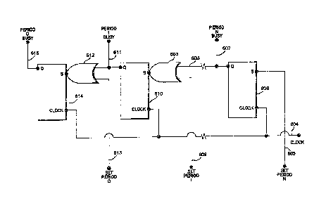
Fig. 6 describes the shift register used in the
preferred embodiment. The address and scalar register
paths are each served by one shift register. The number
of latches within each shift register corresponds to the
longest delay possible between instruction issue and a
result being delivered to the address or scalar
registers.
In Fig. 6, three latches are shown: latch 614
corresponds to the path reservation for clock period 0
after instruction issue; latch 61Q corresponds to the
path reservation for clock period 1 after instruc$ion
issue; latch 606 corresponds to the path reservation for
clock period N after instruction issue. Jagged lines
separate latch 610 and latch 606. The jagged lines
indicate that some number of latches exist within the
shift register between latch 610 and 606. Latch 606
represents the highest delay value possible.
At every clock pulse 604, latch 606 is set by
signal 605, also labelled as Set Period N. If signal 605
is a logical "1", latch 606 is set~ If signal 605 is a
logical '`0", latch 606 is cleared. The output from latch
606 is transmitted to the conflict checking circuits, 24
or 26, via signal 607, also labelled as Period N Busy.
If output 607 is a logical "1", then the path is reserved
at clock period N. If signal 607 is a logical "o", then
the path is available at clock period N. At every clock
pulse 604, the output 607 from latch 606 is transmitted
-8- ~321029
to the next latch in the shift register. Therefore, the
input of each latch at clock time T i9 shifted to the
next latch at clock time T + 1.
At every clo~k pulse 604, latch 610 is set or
cleared by the output of OR gate 608, whose input is
signal 609, also labelled as Set Period 1, and the output
603 from the previous latch. The output ~rom latch 610
i5 transmitted to the conflict checking circuits, 24 or
26, via signal 611, also labelled as Period 1 Busy.
At every clock pulse 604, latch 614 is set or
cleared by the output of OR gate 612, whose input ig
signal 613, also labelled as Set Period 0, and the output
611 from the previous latch 610. The output from latch
614 is transmitted to the conflict checking circuits, 24,
26, via signal 615, also labelled as Period O Busy.
Every latch in the shift register may be
sampled or set at every clock period by the conflict
checking circuits 24 or 26. Note that circuits 24 and 26
must offset the shift register output by 1 because the
delay chain is examined 1 clock period prior to the
instruction issue time.
Fig. 3 describes the conflict checks performed
for the remaining resources, including vector functional
units 32 and 33, local memory access 34, common memory
access 35, and multi-parcel instructions 36.
At phase -9, the instruction word is present in
register 10. Parcel selection by circuit 11 occurs from
phase -8 through phase -7. At phase -6, the instruction
18 enters the decode circuit 13. The decode circuit 13
requires 3 phases to complete. At phase -3, the decode
circuit 13 transmits information 20 to the conflict
checking circuits 32, 33, 34, 35 and 36. A Primary
Conflict signal 37 is generated at phase -2 if a conflict
is detected. If no Primary Conflict signal 37 is
generated, issue occurs at phase 0. At phase +l after
issue, the resource reservation flags are set by circuits
-9- 132~029
32, 33, 34, 35 anfl 36.
Fig. 4 provides a more general description than
the first three drawings. ~t phase -8~ the instruction
word enters the selection circuit 11. The signal Parcel
Select 38 at phase -7 tells the selection circuit 11
which parcel to choose. At phase -7, the instruction
parcel 18 is sent to the decode circuits 12 and 13. At
phase -6, the decoding process begins. At phase -4, the
decoding process is complete and signals 19 and 20 are
generated indicating which resources are requested by the
instruction. At phase -3, conflict checks 14, 15, 24,
26, 32, 33, 34, 35, or 36 begin, comparing resources that
are currently busy or will become busy with the resources
being requested. Primary Conflict signals 22, 28, 29, or
37 are generated at phase -2 if a conflict occursO If a
Primary Conflict is signalled, instruction issue does not
occur at phase 0 and the signal Issue 23 drops. At phase
0, another signal called Secondary Conflict 39 may be
generated. A Secondary Conflict signal 39 mea~s that the
resource conflict that caused the Primary Conflict signal
22, 28, 29, or 37 still exists so instruction issue must
be held.
Therefore, in looX-ahead instruction issue
control, a series of checks are made prior to instruction
issue that can generate a Primary Conflict signal that
causes instruction issue to be held for 1 clock period.
If the conflict is not resolved within that 1 clock
period, a Secondary Conflict signal is generated for
additional clock periods. For every clock period
thereafter, until the conflict is resolved, the Secondary
Conflict signal prevents instruction issue from
occurring. When the conflict is finally resolved, the
Secondary Conflict signal drops and the instruction is
allowed to issue. At that point, +N phases after
instruction issue was first scheduled to occur, the
resource reservation flags are set by instruction issue
132:1~2~
--10--
control.
Fig. 5 describes in more detail the logic
required f~r generating Primary and Secondary Conflicts.
At phase -4, issua occurs for an instruction
that is two instructions ahead of our example instruc-
tion. The latch Issue 501 is set by Issue signal 23 for
one clock period as a result of instruction issue. At
phase -3, Issue 501 sets latch Issue +1 502 for one clock
period. At phase -2, latch Primary Conflict 506 is set
for one clock period by AND gate 505, whose input is
Issue +1 502, Request 503, and Busy 504.
Request 503 represents the operation of
circuits 12 and 13 which output a series of signals that
identify the resource requests of the example
instruction. Busy 504 represents the operation of
circuits 15, 24, 26, 32, 33, 34, 35, and 36 which output
a series of signals that identify which resources are
currently busy and which resources will become busy when
the next instruction is ues at phase -2. The AND
operation at 505 sets Primary Conflict 506 ~or one clock
period if a conflict occurs between the Request 503 and
Busy 504 outputs.
At phase -2, issue occurs for the instruction
immediately ahead of the example instruction and Issue
501 is again set by Issue signal 23 for one clock period.
At phase -1, latch Hold Issue 509 is set for one clock
period by AND gate 508, whose input is Issue 501 and
Primary Conflict 506. At phase -1, Issue +1 502 is set
for one clock period by Issue 501. At phase 0, latch
Secondary Conflict 511 is set for one clock period by AND
gate 510, whose input is Issue +1 502, Request 503, and
Busy 504. At phase 0, Hold Issue 509 prevents
instruction issue for the example instruction by setting
latch No Issue 512 for one clock period. At phase +1,
latch No Issue +1 514 is set for one clock period by No
Issue 512. At phase +1, Hold Issue 509 is set for one
-ll- 1321~2~
clock period by AND gate 513, whose input is No Issue 512
and Secondary Conflict 511. At phase +2, Hold Issue 509
again prevents instruction issue by setting No Issue 512
for one clock period.
Notice that a Secondary Conflict can hold issue
on an instruction only if a Primary Conflict has
occurred. The Primary Conflict prevents instruction
i8su~ at phase o only. Thereafter, as long as a conflict
remains between Request 503 and Busy 504, Secondary
Conflict 511 prevents instruction issue. Once the
conflict is resolved, Secondary Conflict 511 clears. As
a result, Hold Issue 509 and No Issue 512 clear and
instruction issue occur~.
The Primary Conflict actually indicates the
"look-ahead" conflict. In contrast, the Secondary
Conflict prevents an instruction at the issue position
from issuing until all the requested resources are
available. When an instruction is at the issue position
in a prior art machine, it is held until the resource
conflicts are resolved. A Primary Conflict on the other
hand, indicates that the resources are already busy or
will become busy before the instruction issues.
Although a specific configuration circuitry has
been illustrated and described for the preferred
embodiment of the present invention set forth herein, it
will be appreciated by those of ordinary skill in the art
that any arrangement of circuitry which is calculated to
achieve the same purpose may be substituted for the
specific circuitry shown. Thus, the present invention
disclosed herein may be implemented through the use of
different components or in different timing arrangements
then those disclosed in the detailed description. This
application is intended to cover any adaptations or
variations of the present invention. Therefore, it is
manif~stly intended that this invention be limited only
by the claims and the equivalents thereof.