Note : Les descriptions sont présentées dans la langue officielle dans laquelle elles ont été soumises.
BACKGROUND OF THE INVENTION
(Field of the Invention)
The present invention relates to a photoelectric
detector utilizing the light which is projected to and then
reflected on an object to be detected to detect information
such as presence or absence of said object or a distance to
said object.
(Background Art)
There have already been proposed the photoelectric
detectors of various arrangements utilizing the reflected
light from the object to be detected.
In accordance with this prior art, light is
projected from a light emitting diode to an object to be
detected and the light reflected on said object is received
by a phototransistor.
With this photoelectric detector, it is possible
to detect the presence of the object to be detected, so far
as said object is within a distance or range of _, and once
an output threshold has been preset, it is possible to
detect the maximum distance dmaX to the object by
determining when a photoelectric current from said
phototransistor is interrupted.
The above-mentioned detector of prior art,
however, has encountered a serious problem that the
intensity of reflected light depends on the characteristics
of individual objects to be detected, for example, the
reflection factors and the reflecting surface
configurations. Therefore, detection has been
-:
' -
:
13~2~70
inconveniently limited to the particular objects having
certain characteristics because a value of the maximum
distance dmaX depends on said characteristics.
Accordingly, such detector of well known art has
been certainly effective for detection of a distance with
respect to objects of a specific kind (particularly having
a same reflection factor), but less reliable for detection
of objects of different kinds.
10 SUMNARY OF THE INVENTION
The invention relates a photoelectric detector
utilizing the light reflected on an object to be detected
and particularly to such photoelectric detector carried by
a vèhicle such as an automobile to be effectively used as a
back sensor adapted to detect an obstacle as the vehicle is
backed.
A principal object of the invention is to provide
a photoelectric detector which can reliably detect presence
or absence of an object to be detected, a distance to the
object, etc., even when the intensity of reflected light
depends on characteristics of the individual objects to be
detected such as the reflection factor and the reflecting
surface configuration.
This object is achieved, in accordance with the
present invention, by providing a photoelectric detector
comprising first ~ànd second light sources respectively
-having different light
:
'",
~' - `
r~ ~
emitting areas, a photoelectric transducer member adapted to
receive the light emitted from these light sources and then
reflected on an object to be detected, and a signal
processing circuit functioning to separate electric signals
corresponding to said first and second light sources from an
output of said photoelectric transducer member and to
compare these separated two electric signals with each other
so that presence or absence and a position of said object
are detected on the basis of such comparison of said two
electric signals.
This object is also achieved, in accordance to the
present invention, by providing a photoelectric detector
comprising first and second light sources having,
respectively, different light emitting areas, and disposed
to illuminate a common region of an object to be detected,
photoelectric transducer means adapted to receive the light
emitted from said first and second light sources and then
reflected by the object, and a signal processing circuit
functioning to separately process electric signals
corresponding to said first and second light sources from an
output of said photoelectric transducer means and to compare
these two separately processed electric signals to each
other so that presence or absence, and a position, of the
object are detected on the basis of such comparison of said
two electric signals, wherein each electric signal has a
value representative of the intensity, at said transducer
means, of light emitted by a respective light source and
reflected by the object, and said signal processing circuit
compares the intensity-representing values of the two
signals.
Preferably, with this photoelectric detector, the
light projected from the first and second light sources
respectively having different light emitting areas to and
then reflected on an object to be detected is transduced by
l3~7a
the photoelectric transducer member to electric signals
which are then separated into the electric signals
corresponding to the first and second light sources,
respectively, and these separated two electric signals Sa,
Sb are compared to each other in the signal processing
circuit.
Preferably, it is determined that said object to
be detected is within a predetermined distance or range when
the comparison indicates that the one electric signal Sa and
the other electric signal Sb are in relationship of Sa ~ Sb,
and the maximum distance can be detected when a relationship
of Sa = Sb is established. Such feature that two electric
signals respectively corresponding to the first and second
light sources are compared to each other for detection
enables the desired detection to be achieved at a high
precision regardless of characteristics of the object to be
detected, such as the reflection factor and the reflecting
surface configuration.
: . , ,.,.. : .: . , .
, ; . . : .
.~ , . ~., -:
:, :- : . : ::
:., . ~ - :
...,:-,
:.:. .,:. : .
-: ~
2 ~ ~ ~
BRIEF DESCRIPTION OF DRAWING
Figs. 1 through 3 illustrate a principle of the
invention, wherein Fig. 1 illustrates, by way of example, an
arrangement utilizing a square diffusing surfaced source of
light A and a point source of light B for detection, Fig. 2
illustrates, by way of example, another arrangement
utilizing a rectangular diffusing surfaced source of light
A1 and a point source of light B for detection and Fig. 3
illustrates a variation in illuminance of said light sources
A, Al and B relative to a distance;
Fig. 4 is a side view showing an embodiment of the
diffusing surfaced source of light;
Fig. 5 is a front view of said diffusing surfaced
source of light;
Fig. 6 illustrates another embodiment of the
diffusing surfaced source of light comprising the first
light source and a combined therewith plurality of second
light source/light receiving element sets arranged in array;
Figs. 7 through 9 illustrate embodiments of an
electric circuit arrangement for execution of the invention,
wherein Fig. 7 shows a circuit adapted to activate the first
light source and the second light source at different
frequencies, Fig. 8 shows a circuit adapted to activate the
first light source and the second light source at different
wavelengths and Fig. 9 shows a circuit adapted to activate
the first light source and the second light source
alternately; and
Fig. 10 is a schematic circuit diagram
illustrating the conventional photoelectric detector.
. . : , , .
; ;~
.
~ A
DESCRIPTION OF THE DRAWINGS
There have already been proposed the photoelectric
detectors of various arrangements utilizing the reflected
light from the object to be detected, an example of which is
illustrated by Fig. 10 of the accompanying drawing.
In accordance with this prior art, light is
projected from a light emitting diode 11 to an object 12 to
be detected and the light reflected on said object 12 is
received by a phototransistor 13.
With this photoelectric detector, it is possible
to detect the presence of the object 12 to be detected, so
far as said object 12 is within a distance or range of d,
and once an output threshold has been preset, it is possible
to detect the maximum distance dmaX to the object 12 by
determining when a photoelectric current from said
phototransistor 13 is interrupted.
The above-mentioned detector of prior art,
however, has encountered a serious problem that the
intensity of reflected light depends on the characteristics
of individual objects 12 to be detected, for example, the
reflection factors and the reflecting surface
configurations. Therefore, detection has been
inconveniently limited to the particular objects 12 having
certain characteristics because a value of the maximum
distance dmaX depends on said characteristics.
Accordingly, such detector of well known art has
been certainly effective for detection of a distance with
respect to objects of a specific kind (particularly having a
same reflection factor), but less reliable for detection of
objects of different kinds.
;, -;
,
.~
: :: . : :.
`:. :
A more detailed understanding of the invention can
be had from the following description of exemplary
embodiments in reference with the accompanying drawing.
A principle of the invention will be discussed
particularly in reference with Figs. 1 through 3.
Generally, illuminance decreases in inverse
proportion to a distance from a light source and, in the
case of a point source of light, to a square of the
distance. However, such square rule will not be followed
lo when the light source has a rPlatively large surface area
for a predetermined distance from the light source and the
illuminance decreasing factor with respect to the distance
depends on the surface area of the light source.
The present invention utilizes such phenomenon of
lS illuminance variation.
Referring to Fig. 1, _ designates a diffusing
surfaced light source formed in a square of 100 cm X 100 cm.
Now a point O is defined at a vertical distance D cm from a
point P corresponding to one corner of said square and a
horizontal illuminance E at said point O is obtained as
following, based on the boundary integration theorem:
E = L ~ a ~-tan 1 b b tan 1 a ~ (~ x)
2 ~ 2+a2 Id2+a2 d~ 2 ~d2+b2J
where L represents a brightness of the diffusing surfaced
light source _, a represents a length of one side of this
light source _, b represents a length of the other side
thereof and _ = D.
Assumed that an illuminance of the point O at D =
50 cm is 1 (100%) in this calculation formula, the
illuminance varies as the distance D varies, as illustrated
by LO in Fig. 3.
Referring to Fig. 2, A1 designates a diffusing
'.~
" : :
.;;J ~
surfaced light source formed in a rectangle having a long
side of a1 = 50 cm and a short side of b1 = 15 cm. Now a
point P is defined at a longitudinal distance C1 = 30 cm
from said light source A1 and a point Q is defined at a
vertical distance D cm from said point P. An illuminance of
the point Q is calculated by the above-mentioned formula and
the result is shown by LQ1 in Fig. 3. Referring to Figs. 1
and 2, an illuminance of the point 0 varies in inverse
proportion to a square of the distance as shown by LQ2 in
lo Fig. 3, when a point source of light B is placed on the
point P. Assumed, on the other hand, that a light receiving
element P.C is placed at the same position as said point
source of light B and an object to be detected is present at
the point o, the light emitted from the light sources _, B
or A1, B and reflected on said object to be detected is
received by the light receiving element P.C and thus said
object is detected in accordance with the output of said
light receiving element. Specifically, it may be
appreciated that the output of the light receiving element
P.C is associated with the light sources _, B while the
output of said light receiving element P.C is associated
with the light sources A1, B, the object to be detected can
be determined to lie within D = 50 cm if the relationship of
Sa < Sb or Sa1 < Sb is established. It should be understood
here that the output of the light receiving element P.C is
previously adjusted by suitable means such as amplifiers so
as to take respectively same values (Sa = Sb, Sa1 = Sb) at
the specified distance (D = 50 cm).
In such previous adjustment of the light receiving
element output, it is also possible that the light intensity
of any one of the light sources _, B, or any one of the
light sources A1, B is adjusted.
Although the light source B has been assumed to be
the point source of light in the aforegoing description,
' ~.: ~ :
: . .
. -
.. : :
. . , :
, :,
: ~ :
this light source B may be, instead of being the point
source of light, a light source other than the point source
of light so far as it is arranged to have a light emitting
area different from that of the light source _ or A1, since
the present invention has a unique arrangement that two
electric signals are compared to each other, as has
previously been mentioned.
Figs. 4 and 5 illustrate a light source 21 as a
specific embodiment of said light source _ or A1, comprising
a plurality of light emitting diodes 23 arranged in the form
of matrix on a circuit substrate 22 so as to provide a light
source having a large light emitting area.
Such light source may be also realized by
arranging a plurality of electric luminescences (EL) or
fluorescences (FL).
When the light source _ or A1 is embodied in the
form of the light source 21 as shown by Figs. 4 and 5, an
arrangement is also possible in which one of the light
emitting diodes 23 is used as the light source B and there
is disposed the light receiving element P.C such as a
phototransistor adjacent said light emitting diode 23.
Fig. 6 illustrates another embodiment of the
present invention, in which the light source _ or A1 is
formed as an elongated band-like light source 24 including
a plurality of light source B/light receiving element P.C.
sets (B1, P.C1; B2, P.C2;............. ) arranged therein at
several locations.
With this embodiment, to avoid any interference
among the respective light sources B, these light sources
B1, B2, B3,... are successively energized and the
corresponding detections are successively performed by the
respective light receiving elements P.C1, P.C2, P.C3,......
It should be understood that the light source 24 of Fig. 6
may be also arranged not to be lit over the entire area but
;
- . :
J ~ 5 ~
to be lit only over respective areas as defined by shading
lines as shown.
Figs. 7 through 9 are block diagrams illustrating
various embodiments of a circuit arrangement adapted to
5 process electric signals, in which the similar circuit
sections or members are designated by the similar reference
numerals.
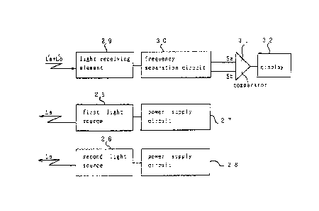
Referring to Fig. 7, reference numeral 25
designates a first light source corresponding to the light
lo source _ or A1, 26 a second light source corresponding to
the light source B and 27, 28 power supply circuits
respectively functioning to energize said light sources 25,
26 at different frequencies. Light rays La, Lb projected
from the respective light sources 25, 26 are reflected on an
object to be detected, and the reflected light rays L'a, L'b
are received by a light receiving element 29.
output signal from the light receiving element 29
is subjected to frequency separation and amplification, then
output as electric signals Sa, Sb.
These two electric signals Sa, Sb are compared to
each other in a comparator 31 and a result of comparison is
sent to a display 32.
The display 32 may be of visual type or acoustic
type.
If the object to be detected or the detector is
moving, there may be provided an arrangement such that the
output of the comparator 31 is utilized to stop this
movement.
Fig. 8 illustrates an embodiment in which the
wavelength of the light emitted from the first light source
25 is different from the wavelength of the light emitted
from the second light source 26, for example, the first
light source 25 is a light emitting diode adapted to emit
red light La and the second light source 26 is a light
.; : ; ' ~ ', '
.
,, . - :
. . , ~
emitting diode adapted to emit infrared light Lb.
Additionally, there are provided a filter 33 adapted to
transmit only the red light and a filter 34 adapted to
transmit only the infrared light in front of the respective
light receiving elements 29 and 35. A block 36 represents
a power supply circuit to drive the light sources 25, 26 so
that the red light La and the infrared light Lb may be
modulated so as to be distinguished from the natural light.
Such modulator means is preferably provided also in the
previously mentioned embodiment in reference with Fig. 7 as
well as in the embodiment as will be described later in
reference with Fig. 9.
In this manner, the red light L'a reflected on the
object to be detected is received by the light receiving
element 29 while the infrared light L'b similarly reflected
on said object is received by the light receiving element
35, and the outputs of these light receiving elements are
applied through amplifiers 37, 38 to the comparator 31 as
the corresponding electric signals Sa, Sb. Then, a result
of comparison is displayed by the display 32 as in the
previously mentioned embodiment.
Fig. 9 illustrates an embodiment in which the
first and second light sources 25, 26 are alternately
energized by a distributor 39, and correspondingly the light
receiving element 29 alternately receives the reflected
light rays L'a, L'b coming from the object to be detected.
A block 40 represents a clock pulse generator to
supply clock pulses to the distributor 39 and a signal
separator 41. The signal separator 41 is responsive to
input of the clock pulse to separate the signal applied from
the light receiving element 29. Two signal series obtained
by such separation are, after integrated, applied through
circuits 42, 43 functioning to amplify the signals to a
predetermined level to the comparator 31 as the electric
: ;. ~. ~ . ' :
,. :' ~ . ::
~l ~P ~
signals Sa, Sb and a result of comparison is displayed by
the display 32 as in the previously mentioned embodiments.
Although the present invention has been described
with reference to specific embodiments, the present
invention is not limited to these specific embodiments. For
example, when the present invention is practically adopted
as a back sensor for automobile, the light source having a
large light emitting area may be utilized as the tail light
to detect any obstacle as an object to be detected during
backing of the automobile.
,, ; :
, , ~. .:. . . . .
. : ~,:: , ; ,,- :- ~. .
:-, ~:
: . ,