Note : Les descriptions sont présentées dans la langue officielle dans laquelle elles ont été soumises.
1 323509
IMPROVEMENTS IN OR RELATING TO DEVICES FOR MEASURING FLUID DENSITY
This invention relates to a device for measuring fluid
density, and in particular to a micro-engineered device
manufactured on a semiconductor substrate.
According to the invention there is provided a device for
measuring fluid density, the device including a structure which
can be made to vibrate in a fluid, means for causing said
structure to vibrate and means for detecting a characteristic of
the vibration, the characteristic being dependent on the density
; of the fluid to be measured.
; 10 In a preferred embodiment, the structure ~ be a
micro-engineered structure, including, for example, a
micro-engineered cantilever beam or leaf structure fabricated on a
substrate of silicon, though other semiconductors or other
materials could be used. The cantilever or leaf could be replaced
by a diaphragm.
The device ~y comprisesa micro-engineered structure
fabricated on a semiconductor substrate wherein the substrate has
a hole extending through the substrate and wherein the
micro-engineered structure is located at one end of the hole.
According to a further aspect of the invention there is
provided a method of measuring fluid density, the method including
causing a structure to vibrate in a fluid and measuring a
characteristic of the vibration, the characteristic being
q~ .
, . . .
,
: -: :
.
''
1 323509
: 2
dependent on the density of the fluid.
An important aspect of this invention is the provision of a
method whereby the fluid density can be measured in said manner
whilst ensuring the effects of changing fluid viscosity are
negligible.
The structure may be driven into vibration by a variety of
forces derived optically, thermally, electrostatically or
- electromagnetically.
In order that the invention may be clearly understood and
readily carried into effect, it will be described by way of
example with reference to the accompanying drawings, of which:
Figure 1 shows a micro-engineered cantilever beam for use as
a density sensor,
Figure 2 shows a schematic plan view of a cantilever beam as
in Figure 1 (end contacts not shown),
Figure 3 represents a leaf for use as a density sensor,
Figure 4 shows a schematic plan view of the leaf of Figure 3,
and
Figure 5 is a schematic representation of a preferred
embodiment of a device according to the invention.
Figure 1 shows a silicon substrate 1 having a
micro-engineered cantilevered beam 2 fabricated on it for use as a
density sensor. The beam is at the end of a tube 5 and has a
contact 3 manufactured on its end and a contact 4 manufactured on
the substrate below the contact 3.
Figure 2 is a plan view of the cantilever 2 of Figure 1 (end
contacts not shown). The sensitivity of the device depends on the
area B of the beam in relation to the surrounding area C. For
greater sensitivity, the ratio of B:C should be large.
Figure 3 represents a leaf 6 manufactured on a substrate 7
supported by side arms 8 and 9. The side arms are anchored at the
ends joined to the substrate. Figure 4 shows a plan view of the
leaf which twists about an axis 10. It is of length W and width A.
The equation of motion for a cantilever or leaf vibrating in
~ ~,
1 3235Q9
: 3
a stationary fluid is described by:
mx + Rx + Kx = FD (i)
where m = effective mass at end of cantilever, or
mass moment of inertia of a leaf
(if the cantilever has a mass on its free end
then m ~ mass on free end + /3 mass of
cantilever, if leaf has a mass on its free and
this should be added to mass moment of inertia).
R = frictional damping constant of fluid in which
the device vibrates,
K = ~spring constant~ of the vibrating structure,
and
FD = any force driving the device into
operation.
X = amplitude of vibration.
The response of such a device with frequency can be derived
from (i) and equals:
x = FD (ii)
CK + W m - 2w2 Rm + R2W2~ 1/2
w = 2Trf where f is the frequency of vibration.
amplitude of vibration (x) will be a maximum when:-
l m - R 2 (iv)
The value of K for the cantilever is given by:
K = Ybt (v)
413
where Y = Young's modulus of elasticity,
b = width of cantilever,
t - thickness of cantilever, and
1 = length of cantilever.
~ ' '
1 323509
: 4
The value of K for the leaf is given by:
K = 2Gdt Ivi)
31
Where G = shear modulus of elasticity,
t = thickness of side arms,
d = width of side arms, and tsee Figure 3)
1 = length of side arms.
The effective mass mL of the leaf for insertion into (ii)
and (iv) is given by:
mL = A W~ t + ~ L d t (vii)
where ~ = density of leaf material, and
d: t, A and W are shown in Figure 4.
If the leaf has an end contact of mass mc at its free end
then m = m + m .
Referring to (iii), if w = wR, (i.e. the structure
vibrated at its resonant frequency) then substitution in (iii)
gives
x = P
D (viii)
WRR
At low pressures, R can be derived from kinetic theory and
is given by:
~ 2~ m (ix)
where~G = density of fluid in which the structure vibrates
k = Boltzmann's constant,
T = absolute temperature,
A = area of vibrating surface, and
ms = mass of gas molecules.
The value of R at higher pressures where the mean free path
of gas molecules is small compared with the dimensions of the
~ . ,
~' ~'' :
1 32350q
: 5
vibrating structure is not clear from the prior literature.
However, a model can be derived which is believed to be
applicable to many devices including those considered herein.
The value of R from this is believed to be:
RG= A~ (2weG ~)1/2 (x)
where ~ = coefficient of viscosity.
For a structure vibrating at its resonant frequency, the
amplitude of vibration is given by expression (ii). However, it
can be seen from expressions (ix) and (x) that the result
obtained depends on the fluid constituents (which determine
viscosity and mass), as well as on the fluid density ~ G.
The device may be made sensitive to gas density but
relatively insensitive to viscosity or molecular mass by
judicious use of the sound waves emitted by the vibrating
cantilever or leaf.
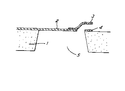
Figure 5 represents a preferred embodiment of a device, in
which the vibrating structure (represented as a beam 13) is
situated at the end of a tube 11 which is open at its opposite
end. The dimensions of the tube are small compared with the
wavelength of sound waves created in the fluid by the vibrating
structure. In the illustrated embodiment the tube is a
rectangular hole in the substrate 12 (which may be silicon~
which can be fabricated using anisotropic etch techniques.
Typically, a rectangular tube may be 200~ m long, 100~ m
wide and 400~ m deep (dimensions p, q and r respectively as
shown in Pigure 5).
Sound waves generated by the vibrating cantilever or leaf
will spread out rapidly in all directions at the open end of the
hole. The gas near the end of the tube reacts on the wave and
exerts a force on the vibrating structure proportional to the
acceleration of the gas in the opening.
The force exerted back onto the vibrating structure is
given by:-
F = i ( S2) ~ C t [ ~ dv (xi)
,
: . ,
1 323509
: 6
where r is length of hole shown in Figure 5, s = area ofvibrating structure, T is cross sectional area of hole, ~ =
wavelength of the sound waves.
A simple expansion of the tan factor and re-arrangement of
terms shows that if ~ is less than 0.3 then (xi) becomes:-
T )~ dt (xii)
consideration of (i) will show that effective mass is now equalto:-
m + ~ ~ GT (xiii)
This value of mass should be inserted in (i), (ii), (iv).
Both resonant frequency and amplitude of vibration are
proportional to gas density ~G~
The motion of the gas in the hole causes an additional
frictional force on the beam given by:-
2 (p + q) r (2U~ ~G) / ~ (xiv)
dt
The frictional constant should be added to R in (i), (ii),
(iv) and (x).
Resonant frequency is now given by:-
R ¦ R - ~ (p + q) r __ln~2 (2
\l 1~G (TJ 3 (XV,
By fabricating a cantilever or leaf of correct dimensions it
has been found that the device may be made sensitive to gas
density, but relatively insensitive to viscosity or molecular
mass, by measurement of the change in resonant frequency (as
described by xv).
Suitable devices can be fabricated by using micro-engineering
techniques. A further advantage of a micro-engineered device is
the fact that it can be fabricated using methods similar to
standard integrated circuit techniques, which leads to low cost
batch production. Further advantages are small size and the fact
.
: -: :. : ::
1 323509
: 7
that sensing circuitry can be included on the same chip as the
density sensor.
The gas density can also be measured by its effect on
amplitude of vibration (x). The frequency at which the amplitude
is measured is chosen to give maximum discrimination between
effects of density and effects of viscosity.
The invention is applicable to measurement of density of
liquids as well as gases, but in the case of liquids the viscosity
term may be more significant.
The driving force for causing the structure to vibrate may be
an electrostatic force applied by providing a sine wave voltage
between contacts fabricated at the end and below the end of the
beam or leaf. Any suitable drive circuit may be used.
In this case the force FD is given by
D IN B (xv)
YB
where VIN = sine wave voltage height,
VB = d.c. bias applied between end contacts,
= permittivity,
A = area of overlap of end contacts, and
YB = gap distance between end contacts.
- It would also be possible to apply a square wave or pulses.
Another way of making a beam or leaf vibrate would be to
apply a pulsed current to a resistive film placed on top of the
beam, and the pulsed heating caused by the current would cause
the beam to vibrate. A further method of making a beam or leaf
vibrate is to apply optical pulses from a laser.
n, ~ The fabrication of a micro-beam and end contacts is
Our ,~ub/~ s J~ed ~3 ~ 703~4
` described in~European Patent Application No. 8$}4ig~6n~-;
End contacts for a leaf can be made in the same way as
described in that application, and the techniques for leaf
fabrication are similar to those for beam fabrication. The leaf
can be made from doped silicon or an insulator. The side arms 8
and 9 can be made from the same material as, or a different
material from, the main mass. Silicon oxynitride (a material
~ ~-
1 32350~
not usually used in integrated circuit fabrication) is a particularly
suitable material for some purposes.
A suitable composition of silicon oxynitride to produce
cantilevers, leaves or side arms showing negligible stress, has
a refractive index from 1.5 to 1.6, and preferably 1.53, and formed
by the reaction between ammonia, silane, and nitric oxide and using
atmospheric CVD techniques.
Another method of producing silicon oxynitride uses ammonia,
silane and nitrous oxide in a low pressure CVD reactor, in which
case the preferred refractive index is 1.8 to 1.9.
A leaf structure may be fabricated on a single crystal p-type
silicon substrate. The main mass of the leaf may be silicon with
silicon oxynitride on top. The silicon leaf can be delineated within
an oxide mask and doped with boron to more than 102 boron atoms/cm3
by either diffusion or ion implantation. The diffused or implanted
depth should be that required to obtain the desired thickness of
leaf. The surface of the substrate is coated with the material
and to the required thickness for the side arms.
The shape of the leaf and side arms is delineated within a
photo-resist pattern and etched out using an anisotropic etch.
The "tube" is etched by masking and anisotropically etching
from the back of the slice. The highly doped silicon and the side
arm material are unaffected by the anisotropic etch.
The amplitude of vibration can be measured directly by incor-
porating a material responsive to stress on the microbeam or sideareas of the flap. Such a material could be, for example, piezo-
electric zinc oxide, or piezoresistive silicon (either polycrystalline
or single crystal) and doped to obtain the desired characteristics.
The amplitude of vibration can also be measured by the variation
in capacitance between the end contacts on the beam and below it.
,~,: . .: .:
.. ~