Note : Les descriptions sont présentées dans la langue officielle dans laquelle elles ont été soumises.
g 9
-- 1
AGC D~LAY ON AN IN~GRA~D CIRC~IT
FIELD OF THE INVENTIO~
The present invention relates to radio
receivers, and more particularly relates to the
automatic gain control (AGC) circuitry used in such
receivers.
BACKGROUND AND SUMMARY OF THE INyENTIoN
Many radio receivers and amplifiers have an
AGC feature for reducing the amplification of one or
more gain stages to compensate for the varying levels
of signal intensity that may be received. Such AGC
circuits permit modern receivers to have dynamic
ranges in excess of 100 dB.
In certain applications, particularly at high
frequencies and low signal strengths, the noise figure
of the receiver becomes an important consideration.
The receiver noise figure is most directly affected by
the gain of the receiver front end. Consequently, it
i8 desirable to operate the front ends of sensitive
receivers at maximum gains and to gain control
subsequent stages. Only after the received signal
strength is so large that noise figure is not an
important issue should gain reduction occur in the
front end stage.
Prior art systems typically address the noise
figure problem by running the front end stage without
any gain control whatsoever. While optimizing the
noise figure, such an approach degrades the overall
system dynamic range since signals above a certain
threshold overwhelm the receiver. Thus, there is a
continuing need for improved AGC systems that will
progressively reduce the gain of the amplifier stages,
beginning with those stages most remote from the front
end.
,', . '
.
.
1 323~q
-- 2
Accordingl~, it is an object of the present
invention to provide an improved AGC system for
receivers which will progressively reduce the gain in
the amplifier stages, beginniny first with the stages
most remote from the front end.
It is a further object of the present
invention to provide such an improved AGC system with
a high degree of noise immunity.
It is still a further object of the present
invention to provide such an improved AGC system that
can be fully implemented using integrated circuit
fabrication techniques.
According to the present invention, the
staggering of the onset of gain reduction in a series
of cascaded gain stages is effected by controlling the
area ratio between corresponding components in two or
more AGC control circuits whose topologies are
otherwise similar. A representative AGC control
circuit may include two transistors in a differential
common-emitter configuration. The bases of the
transistors are driven from a signal related to the
amplitude of signal being received by the receiver.
The collectors of the transistors provide a
differential AGC output signal controllably offset
from the input signal by a voltage determined by the
area ratio between the two transistors. The
differential configuration is preferably employed to
reject common mode signals and thus to improve noise
immunity. Several such AGC circuits can be employed
to cause different amplifier stages in the rec0iver to
begin significant gain reduction at different received
signal thresholds.
The foregoing and other objects, features and
advantages of the present invention will be more
readily apparent from the following detailed
1 32365~
_ 3 --
description, which proceeds with reference to the
accompanying drawings.
BRIEF DESCRIPTION OF THE DRAWINGS
Fig. 1 is a block diagram showing an exemplary
receiver configuration employing the AGC control
system of the present invention.
Fig. 2 is a chart showing gain reduction in
first and second cascaded gain stages as a function of
received signal strength in a receiver using an AGC
circuit according to the present invention.
Fig. 3 is an electrical schematic diagram of
an AGC circuit according to the present invention.
Fig. 4 is an alternative receiver
configuration employing an AGC system according to the
present invention.
Fig. 5 is an electrical schematic diagram showing AGC
circuitry to control two stages independently.
Fig. 6 is a schematic diagram showing the AGC
circuitry of the present invention fabricated in integrated
circuit form.
DESCRIPTION
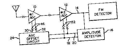
Referring to Fig. 1, a basic receiver topology
is illustrated which includes first and second
cascaded amplifier stages 10, 12. In a typical
embodiment, amplifier 10 may be the RF front end stage
and amplifier 12 may be one or more amplifiers in the
IF amplifier. Coupled to an output 14 of ampli-fier 12
is an amplitude detector stage 16. Amplitude detector
stage 16 produces a differential output signal on
first and second output lines 18, 20, the magnitude of
which is related to the amplitude of the signal output
from amplifier stage 12.
In the embodiment illustrated in Fig. 1, the
output signal provided on lines 18 and 20 is applied
directly to an AGC input 22 of second amplifier stage
12. As the signal on lines 18, 20 increases, the gain
~ 323659
- 4 -
of second amplifier stage 12 decreases, thereby
reducing fluctuations in the output signal provided to
line 14.
(For purposes of the present discussion, it is
assumed that the amplifier stages 10, 12 are designed
to begin substantial gain reductions when the AGC
voltages applied thereto exceed zero volts. In an
exemplary embodiment, the gain at zero volts AGC may
be from zero to three dB below maximum, a value still
considered relatively insignificant.)
As noted in the Background discussion, it is
desirable that the gain of second amplifier stage 12
be reduced prior to the reduction of gain in amplifier
stage 10 if system noise figure is to be optimized.
The chart shown in Fig. 2 illustrates an exemplary
relationship between the AGC signals applied to the
first and second amplifier stages to accomplish this
effect. As can be seen, the first amplifier stage 10
does not have any significant gain reduction when the
signal from amplitude detector 16 is below a threshold
indicated as VO. In this range, however, the second
amplifier stage 12 steadily reduces its gain as the
signal from amplitude detector 16 increases. By this
arrangement, first amplifier 10 operates at
substantially full gain until the received signal
strength is large enough that system noise figure is
not important. Only after the signal exceeds the
threshold indicated by VO do both amplifier stages
reduce gain.
In this example, the slope of the line
indicating the gain reduction in second amplifier 12
is solely a function of the amplifier'~ response to
AGC signals. The slope of the line indicating the
gain reduction in first amplifier 10, however, can be
controlled by the transfer characteristics of the AGC
- - :
- 1 323659
_ 5
control circuit that provides the AGC voltage to the
first amplifier.
Returning to Fig. 1, it can be seen that the
AGC input 22 of second amplifier stage 12 is driven
directly from the output of amplitude detector 16.
Consequently, second amplifier stage 12 begins AGC
control without any threshold. An AGC control circuit
; 24, however, is connected to lines 18 and 20 and
delays the onset of significant gain reduction in
first amplifier stage lO until the signal from
amplitude detector 16 exceeds the threshold V0 shown
; in the chart of Fig. 2.
Fig. 3 shows an electrical schematic
representation of AGC control circuit 24. This
~ 15 circuit comprises first and second transistors 26, 28
;~ arranged in a differential configuration with an
optional gain setting element 29 coupling the
emitters. The bases of transistors 26, 28 are driven
from lines 18, 20 from amplitude detector 16. The AGC
output signals are provided from the transistor
collectors to output lines 30, 32.
In most differential amplifier topologies, the
; circuitry is symmetrical, producing a mirroring of the
currents in the two complementary halves 34, 36. In
the present invention, however, the complementary
halves are not identical. Instead, in the preferred
embodiment, one of transistors 26, 28 has a saturation
current different from the other.
Reverting a minute to circuit theory, a
fundamental relationship in transistor design is that:
V}~e = Vt ln(Ic/I~)
where Vt is a thermal voltage constant (0.026 volts at
room temperature), Ic is collector current and I~ is
the saturation current of the transistor device.
t
.
1 32365q
- 6 -
Since the difference in voltage between lines 18 and
20 is equal to the difference in V~between
transistors 26 and 28, the above equation makes clear
that:
Vbn = VT ln (saturation current ratio~.
If the circuit of Fig. 3 is to produce a zero
volt output signal on its differential output lines
30, 32, the collector currents of transistors 26 and
28 must be equal (assuming the circuits 34, 36 are
otherwise identical). The collector currents will be
equal when the differential voltage applied on lines
18, 20 is equal to the V~. value above. Thus, in an
exemplary system using transistors having saturation
15 current ratios of 2:1 operating at room temperature,
the signal applied to input lines 18, 20 required to
produce a zero volt output signal on lines 30, 32 is
eighteen millivolts.
Returning again to Fig. 1, it can be
appreciated that an AGC signal of up to eighteen
millivolts can be present on lines 18, 20 (and thus
applied to reduce the gain of second amplifier stage
12) before the AGC signal applied to first amplifier
stage 10 rises above zero volts. By this offsetting
arrangement, AGC action in the two stages is staggered
relative to each other as a function of received
signal strength.
In alternative embodiments, it will be
recognized that a similar effect can be achieved by
varying the ratios of other components in
complementary circuits 34, 36, such as the ratios
between collector loads 38 and 40 (which in the
illustrated embodiment have values of 1 kilohms), or
between current sources 42 and 44 (which in the
illustrated embodiment provide constant currents of
100 ~A). In integrated circuit fabrication of the
-
.
~ 3236~9
-- 7
circuit (the preferred construction technique) such
ratios are more readily controlled than the absolute
value of any particular circuit component.
Returning to Fig. 1, it will be recognized
that second amplifier stage 12 i8 AGC controlled
directly from the output of amplitude detector 16.
Thus, second amplifier stage 12 will begin gain
reduction when any signal is present. In most
applications, however, it i8 desirable to delay the
onset of gain reduction, even in second stage 12,
until the received signal exceeds a first threshold.
To achieve this end, gain stage 12 can be designed to
ignore AGC signals below a predetermined threshold.
An alternative approach is to include an AGC control
circuit such as that illustrated in Fig. 3 within
amplitude detector 16 so that a gain reducing signal
does not appear on lines 18 and 20 until the amplitude
of signal output by second amplifier 12 exceeds a
predetermined threshold. Illustrated AGC control
circuit 24 can then be cascaded onto the output of the
AGC control circuit in the amplitude detector 16.
Still another technique for effecting the AGC
staggering result is to use the arrangement shown in
Fig. 4. In this system, the output signal on lines
18, 20 from amplitude detector 16 is not applied
directly to AGC inputs 22 of second amplifier stage
12. Instead, an AGC control circuit 24', such as that
shown in Fig. 3, is interposed. AGC control circuit
24' can be designed, for example, with a 2:1 area
ratio so that the circuit does not provide a gain-
reducing signal to second amplifier stage 12 until the
signal on lines 18, 20 exceeds eighteen millivolts.
A separate AGC control circuit 24" can be
interposed between lines 18, 20 and the AGC inputs 46
of first amplifier stage 10. AGC control circuit 24"
should have an area ratio in excess of the 2:1 ratio
- 8 _ 1 323 659
used by stage 24' so that a gain-reducing signal is
not applied to the first amplifier stage 10 until the
signal on lines 18, 20 exceeds, for example, 50
millivolts.
It will be recognized that either of the
foregoing arrangements (cascading one AGC control
circuit after another, or operating several AGC
control circuits from a common input signal) can be
extended to use with an arbitrarily large number of
gain stages. It will also be recognized that the
present invention can be incorporated as an integral
part of a gain stage and need not appear as a separate
circuit element. By using such a construction
technique, the same line~ 18, 20 can be run to all of
the gain stages, and the responses of the gain stages
will depend on the area ratios of the transistors used
therein.
While the AGC control circuit of Fig. 3 can be
replicated as many time as there are stages needing
different AGC voltages, the circuit of Fig. 5 can
alternatively be used. It will be recognized that the
transistors Q1 and Q2 in Fig. 5 are arranged in
substantially the same fashion as are the transistors
in Fig. 3. The AGC control voltage for the first
gain-controlled stage is taken from their output
terminals.
A second AGC voltage is produced in Fig. S by
making a double use f Q2. That is, a second AGC
control circuit i8 formed simply by adding one more
transistor, Q3, to the circuit and taking the second
AGC voltage from the outputs of Q2 and Q3. (This
arrangement assumes, of course, that the current drawn
by the gain-controlled amplifiers from the AGC lines
i8 negligible so as to not upset circuit operation).
The topologv used in Fig. 5 again is shown
with an optional gain determining resistor R8a1n1
1 3236~9
interposed between the emitters of transistors Q1 and
Q2. The ratio of the load resistors ZL1~ ZL2 to
can be selected to control the slope of the gain
reduction curve (i.e. such as those shown in Fig. 2),
and thus the rate at which gain reduction occurs for a
given change in received signal strength.
Most FM communications receivers are typically
not gain controlled. Instead, their amplifiers are
run at maxi~um amplification and gain control is
effected by hard clipping or limiting of the amplified
signal. It has been found in the present application,
which uses a relatively small aperture antenna in a
wristwatch paging receiver, that the effects of
multipath are minimized if the receiver is gain
controlled rather than relying on typical FM limiter
technology.
As noted earlier, the preferred embodiment of
the inventlon is to use integrated circuit
construction on a common substrate. Although IC
; 20 fabrication techniques do not allow precise control
over individual component characteristics, verv good
control can be obtained between the ratios of certain
components. It is the controlled ratioing between
components that permits the characteristics of the
present invention to be accurately tailored, not the
absolute value of any component per se.
From the foregoing, it will be recognized that
the present invention can accurately and repeatably
sequence the onset of gain reduction in a series of
gain controlled amplifiers implemented on an
integrated circuit for the purpose of maximizing the
dynamic range of the resultant amplifier chain. This
sequencing, or delaying the onset of gain reduction to
the input stage.
Having illustrated the principles of my
invention with reference to a preferred embodiment and
1 323659
-- 10 --
several variations thereof, it should be apparent to
one of ordinary skill in the art that the invention
can be modified in arrangement and detail without
departing from such principles. For example, while
differential circuitry has been illustrated and is
preferred for purposes of noise immunity, the
principles of the invention can also be practiced
using single-ended circuit topologies. Likewise,
while the diagramc have showed the AGC control
circuits configured as common emitter amplifiers,
other topologies, such as common base amplifiers,
could alternatively be used. Similarly, diodes can be
used for loads 38 and 40 in Fig. 3 to introduce a non-
linear effect into the circuit's response. Finally,
the use of the present invention in an FM receiver is
illustrative only, since it is equally useful in a
variety of other receiver and amplifier designs.
Accordingly, I claim as my invention all such
modifications as may come within the scope and spirit
- 20 of the following claims.
:.~
': ' ' ' '
'