Note : Les descriptions sont présentées dans la langue officielle dans laquelle elles ont été soumises.
:
?
;' .
~ '
,f
.'
~'
r
RECEIVE COUPLER FOR BINARY
DATA COMMUNICATION SYSTEMS
Technical Area
his invention relates to binary data
communication and, more particularly, to the communication
of binary data between a plurality of terminals connected
together vla a common data bus.
sackqround of the Invention
While this invention was developed for use in
communicating data between various avionic systems and
subsystems that need to share data, and is described in
such an environment, it is to be understood that the
invention can be utilized to communicate binary data in
other environments. It is also to be understood that while
the invention was developed for use with a current mode
data bus, and is described in connection with such a bus,
the invention can be utilized in connection with other
types of data buses to improve the operation thereof, in
particular, voltage mode and optical data buses.
2~ Similarly, while the invention was developed for use in a
data communication system wherein the binary data to be
communicated is in Manchester biphase form, it is to be
understood that the invention can be used with binary data
coded in other rectangular forms, such as binary data coded
in mark-space form.
In modern aircraft, it is desirable to
integrate, as far as possible, the functions of previous
wiring-independent avionic systems to permit an attendant
reduction in the weight, space and power requirements of
~ . ' ' ' ~
the avionic systems, and to permit a simplification in
wiring between physically separated avionic systems or
subsystems thereof. Such integration has been achieved by
the use of a common data bus to which each avionic system,
or a subsystem thereof, has access through an associated
terminal, each of which is capable of transmitting and
receiving data. The data tranfimitted on the data bus by
one terminal associated with a particular system or
subsystem can be received by the terminals associated with
remaining systems or subsystems, thus eliminating the
requirement for separate wiring interconnections between
the 6ystems or subsystems. In addition, data generated by
a particular system or subsystem can be used by any other
~ystem or subsystem wlthout the necessity of having to
independently generate that data.
While various types of communication systems
that have been developed for use on-board aircraft to
communicate between avionic systems and subsystems, as
described in U.S. Patents 4,199,663 and 4,471,481, both
entitled "Autonomous Terminal Data Communicatlons System"
and assigned to the assignee of the present application,
the most desirable avionic data communication system is an
autonomous terminal data communication system, in
particular, an autonomous terminal data communication
system that uses a current mode data bus. Items critical
to the operation of a data communication system that
utilize~ a current mode data bus are the reliability of the
bus cable and the efficiency and reliability associated
with the way each terminal is coupled to tha bus. Current
mode data bus coupling efficiency and reliability is
addressed in U.S. Patent No. 4,264,827 entitled "Current
Mode Data Or Power Bus," also assigned to the assignee of
the present application. The essence of the invention
described in this patent is a coupling transformer having a
ferrite core designed such that the core can be
disassembled and two wires of a bus formed by a pair of
twisted wires placed around the legs of the core in such a
way that 'the magnetic path of the reassembled core
. ~ ,
surrounds the conductors. The arrangement i~ such that the
bus wires form one of the windings of a transformer. The
other winding is permanently installed on the core and is
connected to the data transmitter and/or receiver
electronics of a data terminal. The end re~ult is the
establishment of current coupling without the need to cut
the bus wires or to remove or perforate the in~ulation that
surrounds the wires.
Another item critical to the successful
operation of a data communication system is the ability of
the receiver electronics to accurately reproduce data
signals carried by the data bus. If the signals are not
accurately reproduced, they may be erroneously interpreted
by utilization devices connected to the output receiver
electronics. In this regard, data signals are frequently
transmitted in rectangular form. An example of a
rectangular data signal is a Manchester biphase data
signal. Ideally, each transition of a rectangular wave
data signal between signal levels is instantaneous.
Unfortunately, the ldeal does not exist. Rather,
transitions between signal levels are exponential, with the
time constant of the exponentlal transition being dependent
upon the lmpedance characteristics of the data bus carrying
the signal and the coupler that couples the data
transmitter to the data bus. More specifically, a8 shown
in FIGURE 1, the bus signal, which represents transmitter
generated Manchester biphase signals reproduced across the
output terminals of a receive coupler transformer of the
type described above, are not sharp. Rather, the
transitions exponentially change over a discrete period of
time.
In the past, bus signals of the type illustrated
in FIGURE 1 have been detected by a pair of oppositely
biased comparators. The bias level is shown by the dashed
lines located above and below the zero signal line of the
bus signal section of FIGURE 1. The outputs of the
receiver comparator are shown on the receiver comparator
lines of FIGURE 1. ~hile the mark-space transitions of the
1 ~ 3
outputs of the receiver comparators are sharp, the
comparator outputs are not an accurate reproduction of the
originally transmitted Manche6ter biphase signal. Rather
than being complementary, a gap exlsts between transltions
of the comparator outputs. That is, both comparator
outputs are at a common low level for a short period of
time between the high-low transition of one comparator and
the low-high transition of the other comparator. The
length of the gap is related to the exponential transition
time of the bus signal. This gap is commonly eliminated by
downstream reconstruction circuits that respond only to the
leading edges of the comparator output signals. As a
result, the high-low transition of one biphase signal does
not occur until the low-high transition of the other
biphase signal. The result of thls reconstruction is shown
in the last lines of FIGURE 1, which also illustrates the
disadvantage of this approach, namely that the duty cycle
of the first cycle of the data signal, in this case the
sync pattern of the Manchester biphase signal, ls not fifty
percent. Rather, the first half of the mark-space cycle,
denoted M1, is greater than the second half, denoted N1.
As a result, the receive coupler reconstructed Manchester
biphase slgnal, RXI and ~XN, does not accurately represent
the transmitter generated Manchester biphase signal, TXO
and TXN. This dlfference can lead to an erroneous
interpretation of the output of the receive coupler by the
utilization device to which it is connected. The invention
is directed to providing a receive coupler that over¢omes
this problem.
Summary of the Invention
In accordance with this invention, a receive
coupler for a binary data communication system that
transmits signals in rectangular form on a data bus is
provided. The receive coupler lncludes a transition and
polarity detector that differentiates received signals and
produces an output pulse on one or the other of two output
lines for each transition of the received signal, the
output line being dependent upon the rise-fall direction of
l~k~ 3
the transition. That is, rise transitions create pulses on
one output line and fall transitions create pulses on the
other output line. The recei~e coupler also includes
reconstruction logic connected to the output lines of the
transition and polarity detector that reConstructs the
received signal based on the pulses.
In accordance with further aspects of this
invention, the data bus signals are in electromagnetic form
and the receive coupler includes a transformer that couples
the data bus to the transition and polarity detector.
In accordanae with further aspects of this
invention, the receive coupler includes a receiver
amplifier connected between the receive coupler transformer
and the transition and polarity detector that amplifies
received rectangular form data signals prior to their rise-
fall transitions creating pulses.
In accordance with further aspects of this
invention, the transition and polarity detector includes
two differentiator-comparator combinations, one differen-
tiator-comparator combination for differentiating rise
transitions of the rectangular data signals amplified by
the receiver amplifier and producing a pulse for each rise
transition above a predetermined level and the other
differentiator-comparator combination for differentiating
fall transitions of the rectangular data signals amplified
by the receiver amplifier and producing a pulse for each
fall transition above a predetermined level.
As will be readily appreciated from the
foregoing description, the invention provides a receive
coupler that is significantly more accurate than receive
couplers that utilize a pair of opposltely biased
comparators to reconstruct a rectangular wave data signal
transmitted on a data bus. The receive coupler of the
invention iB more accurate becau~e the transition related
pulses occur precisely at the same point with respect to
each transition. As a result, the reconstructed receive
signals preclsely replicate the originally transmitted
signal. While the invention iB ideally suited for use in
,
-- 6 --
connec~ion with electromagnetic, e.g., current mode and
voltage mode, data buses, it is also useful in connection
with other types of data buses, such as optical data buses
since the receivers of optical data buses also produce
rectangular wave data signals having exponentially changing
transitions, rather than instantaneously changing
transitions.
Brief Description of the Drawinqs
.
The foregoing and other features and advantages
of the present invention will become more readily
appreciated as the same becomes better understood by
reference to the following detailed description when ta~en
in con~unction with accompanying drawings wherein:
FIGURE 1 is a series of waveforms illustrating
the problems associated with prior art type mark-space
receive couplers designed for use with data bus
communication systems;
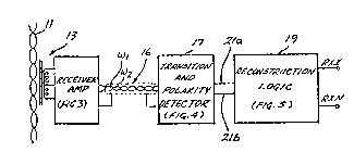
FIGURE 2 is a block diagram of a receive coupler
formed in accordance with the invention;
FIGURE 3 is a schematic diagram of a receiver
amplifier suitable for use in the receive coùpler
illustrated in FIGURE 2;
FIGURE 4 is a schematic diagram of a transition
and polarity detector suitable for use in the receive
coupler illustrated in FIGURE 2;
FIGURE 5 is a block diagram of reconstruction
logic suitable for use in the receive coupler illustrated
in FIGURE 2; and,
FIGURE 6 is a series of diagrams showing the
signals at various points in the receive coupler
lllustrated in FIGURES 2-5.
Description of the Preferred Embodiment
FIGURE 2 illustrates a receive coupler formed in
accordance wlth the invention coupled to a data bus 11.
The receive coupler includes: a transformer 13; a receiver
amplifier 15; a receive stub 16 formed of a shielded pair
of twlsted wires designated W1 and W2; a transition and
polarity detector 17; and, reconstruction logic 19. The
lllustrated da~ bus 11 is a current mode data bus formed
by a twisted pail of wires. The twisted pair of wires form
the primary windings of the recelve coupler transformer 13
which, preferably, is constructed in the manner described
in U.S. Patent No. 4,264,827, referenced above. In
accordance with the inventlon, the secondary wind~ng of the
receive coupler transformer 13 iB connected to the input of
- the receiver amplifler 15, which amplifies rectangular wave
data slgnals (such as Manchester biphase data ~ignals)
carried by the data bus 11 and detected by the receive
coupler transformer 13. The amplified signals are applied
to the transition and polarity detector 17 via the receive
stub 16, which may be relatively long -- up to fifty (50)
feet. The transition and polarity detector 17
differentiates the amplified signals it receives via the
stub and produces pulses on a pair of output lines 2la and
2lb. A pulse is produced for each transition of a
rectangular wave data signal amplified by the receiver
amplifier, which output line 2la or 2lb carries the pulses
determined by the rise-fall direction of the transition.
That is, rise transitions create a pulse on one output
line 2la and fall transitions create a pulse on the other
output line 2lb.
The two output lines 2la and 2lb of the
transition and polarity detector 17 are each connected to
an input of the reconstruction logic 19. The
reconstruction logic 19 reconstructs rectangular wave data
signals detected by the receive-coupler transformer 13 in a
manner that accurately replicates the originally
transmitted rectangular wave data æignals. The end result
is rectangular form data signals having substantially
instantaneous rise and fall transitions.
FIGURE 3 is a schematic diagram of a receiver
amplifier suitable for use in the embodiment of the
invention illustrated in FIGURE 2. The receiver amplifier
illustrated in FIGURE 3 comprises: a depletion type JFET
(junction field effect transistor) designated Q1; two PNP
transistors designated Q2 and Q3; two NPN transistors
~ .
- 8 - ~ b
de~ignated Q4 and Q5; a ~ener diode designated ZD; three
capacitor~ deslgnated C1, C2 and C3; and, fourteen
resistors designated Rl through R14.
One end of the secondary wlnding of the receive
coupler transformer 13 is connected to the emitter of Q2
and to the source terminal of Q1. The other end of the
secondary winding of the receive coupler transformer 13 is
connected to the elnitter of Q3 and to the drain terminal of
Q1. The center of the secondary wlnding of the receive
coupler transformer 13 is connected through Rl to ground.
The gate terminal of Q1 is connected to a negative voltage
bus designated -V1 and to the anode of ~D. The cathode of
ZD is connected to ground. -V1 is supplied by the
tran~ition and polarlty detector via W1 and W2 of the
receive stub 16 in the manner hereinafter described.
The base of Q2 is connected through R2 in series
with R7 to -V1. The collector of Q2 is connected through
C1 to the base of Q4 and through R3 to the junction between
R2 and R7. R4 and RS are connected in series between
ground and the junction between R7, R3 and R2. The
junction between R4 and R5 is connected to the base of
Q4. The emitter of Q4 i6 connected through R6 to the
junction between R7, R4, R3 and R2. The collector of Q4 is
connected to ground.
The base of Q3 is connected through R8 in series
with R13 to -V1. The collector of Q3 is connected through
C2 to the base of Q5 and through R9 to the junction between
R8 and R13. R10 and R11 are connected in serie~ between
ground and the junction between R13, R8 and R9. The
30 .junction between R10 and R11 is connected to the base of
QS. The emitter of Q5 is connected through R12 to the
~unction between R8, R9, R10 and R13. The collector of Q5
is connected to ground. The bases of Q2 and Q3 are also
connected through C3 in parallel with R14 to ground. One
of the outputs, designated W1, occurs at the junction
between R2, R3, R4, R6 and R7 and the other output,
designated W2, occurs at the ~unction between R8, R9, R10,
R12 and R13.
i3 ~ ~)
Q2 and Q3 and their biasing re~istors form low
input impedance amplifiers that amplify in a differential
manner rectangular wave 6ignals produced across the output
of the secondary winding of the receive coupler
transformer 13. The biasing network formed by R2 and R8
with R14 and C3 in combination with R1 control the
` quiescent current flow through Q2 and Q3 in essentially
equal proportions. Differential signals of one polarity
increase the current flow through Q2 while decreasing the
current flow through Q3 and vice versa for differential
~ignals of the opposite polarity. The signals produced at
the collectors of Q2 and Q3 are connected by emitter
follower drivers formed by Q4 ana Q5 and their related
blasing resistors to the outputs W1 and W2 of the receiver
IS amplifier 15.
Preferably, the turns ratio between the data
bus 11 and the secondary winding of the receive coupler
transformer 13 is relatively hlgh ~ 20, for e~ample.
While a hlgh turns ratio results in the current flow in the
secondary winding being relatively small when a rectangular
wave data signal i8 present on the data bus, a large turns
ratio has the advantage of applying a relatively small load
impedance to the data bus. The low load result is enhanced
by the fact that Q2 and Q3, which form grounded base
transistor amplifiers, have small input impedances.
The low input impedance grounded base transistor
amplifiers, i.e., Q2 and Q3 and their associated biasing
resistors, convert the relatively low signal curr~nts drawn
by Q2 and Q3 into relatively high signal voltages at the
collectors of Q2 and Q3. The emitter follower stages,
formed by Q4 and Q5 and their associated biasing resistors,
couple the outputs of the grounded base transistor
amplifier circuits to the wires W1 and W2 of the receiver
stub 16, which connects the receiver amplifier 15 to the
transition and polarity detector 17. The emitter follower
stage transistors, Q4 and Q5 and their associated
resistors, are chosen to create a receiver amplifier output
.
- 10 -
impedance that matches the characteristic impedance of the
receiver stub 16.
FIGURE 4 is a schematic diagram of a transition
and polarity detector formed in accordance with the
invention and suitable for use in the receive coupler
illustrated in FIGURE 2. The transition and polarity
detector illustrated in FIGURE 4 compr~ses: a transformer
- designated Tl; two operational amplifiers designated O~1
and OA2; six capacitors designated C9 through C9; two
diodes designated D1 and D2; and, eight resistors
designated R15 through R22. Stub wire W1 is connected to
one end of the primary winding of T1 and stub wire W2 is
connected to the other end of the primary winding of T1.
The center of the primary winding of Tl is connected to the
negative voltage source, designated -V2, which supplies
power to the receiver amplifier via the stub 16.
One end of the secondary winding of T1 is
connected to ground. The other end of the secondary
winding of T1 is connected through C4 to the inverting
lnput of OA1 and through C5 to the inverting input of
OA2. R15, R16, R17 and R18 are connected in series in that
order between a positive voltage source designated +V3 and
a negative voltage source designated -V3. Even though
their polarities are different, the magnitude of +V3 and
-V3 are the same. The junction between R15 and R16 is
connected to the inverting input of OA1 and the junction
between R17 and RlU is connected to the inverting input of
OA2. The junction between R16 and R17 is connected to
ground.
C7 is connected between the inverting and
noninverting inputs of OA1. The output of OA1 is connected
through C6 in series with R19 and R20 to ground. The
junction between R19 and R20 is also connected to the
noninverting input of OAl. The junction between C6 and R19
is connected to the cathode of D1 and the anode of D1 is
connected to ground. C9 is connected between the inverting
and noninverting inputs of OA2. The complementary output
Of OA2 is connected through C8 in series with R21 and R22
to ground. The ~unction between R21 and R22 i8 connected
to the inverting input of OA2. The junction between C8 and
R21 is connected to the cathode of D2 and the anode of D2
is connected to ground.
As will be readily appreciated from the
foregoing description, the RC networks connected to the
inputs of OA1 and OA2 form differentiators that produce
spike-shaped pulses as shown in the differentiated bus
signal line of FIGURE 6. The biasing networks formed by
10 R15 and R16 connected between +V3 and ground and by R17 and
R18 connected between -V3 and ground provide threshold
voltages as indicated by the dashed lines in the
differential bus signal line of FIGURE 6. More
specifically, the threshold voltage of OA1 is shown by the
lower dashed line and the threshold voltage of OA2 is shown
by the upper dashed line. OA1 is thus made insensitive to
pulses caused by rising transitions of the rectangular wave
signals and OA2 is made insensitive to pulses caused by
falling transitions. Hence, OA1 is only sensitlve to above
threshold pulses caused by falling transitions and OA2 is
only ~en~ltlve to above threflhold pulses caused by rising
tran~itions.
~ he RC networks conneoted to the outputs of OA1
and OA2 reRult in the creation of monostable multivibrators
that stretch pulses produced at the inputs of OA1 and OA2
as a result of the differentiation. The output of OA1 is
applled to wire 2la and the output of OA2 is applied to
wire 2lb. As previously discussed with respect to
FIGURE 2, wires 21a and 21b connect the transition and
polarity detector 17 illuætrated in FIGURE 4 to the
reconstructlon logic.
FIGURE 5 is a block diagram of reconstruction
logic suitable for use in the receive coupler illustrated
in FIGURE 2. The reconstruction logic illustrated in
FIGURE 5 comprises: four three-input AND gates designated
Gl, G2, G3 and G4; six two-lnput AND gates designated G5
through GlO; one four-input OR gate designated G11; three
two-input OR gates designated G12, G13 and G14; six D flip-
- 12 -
.--~
flops designated FF1-FF6; two inverters designated I1 and
I2; and, a two 6tage binary counter designated CT. The
logic diagram illustrated in FIGURE 5 utilizes convention
;
negation symbology. In this regard, G1, G2 and G9 each
5 have one negation input and G3 and G4 each have two
negation inputs.
The output 2la of O~1 of the transition and
polarity detector illustrated in FIGURE 4 is connected to
one input of G1 and to one input each of G5 and G6. The
L 10 output 2lb of OA2 is connected to one input of G2 and to
one input each of G7 and G8. The output of G1 is applied
. to the D input of FF1 and the ~ output of FF1 is applied to
a second input of G1. The Q output of FF1 is applied to
; the second input of G5, one input of G12, a negation input
15 Of G4 and one input of Gl4. The output of G2 is applied to
the D input of FF2 and the ~ output of FF2 is applied to a
: second input of G2. The Q output of FF2 is applied to one
input of G8, a negation input of G3, one input of G13 and
the second input of G14.
The outputs of G5, G6, G7 and G8 are each
applied to one input of G11. The output of G1~ is applied
to the D input of FF3. The Q output of FF3 ls applied to
the negation input of G1, the negation input of G2 and the
second inputs of G6 and G7.
The output of G3 is applied to the second input
of G12 and the output of G12 is applied to the D input of
FF4. The Q output of FF4 is applied to the input of I1 and
to the non-negation input of G3. The output of G4 i8
applied to the second input of G13 and the output of G13 is
3~ applied to the D input of F~5. ~he Q output of FF5 is
applied to the input of I2 and to the non-negation lnput of
G4. One receive coupler output signal, RXI, 18 formed at
the output of I1 'and the other receive coupler output
signal, RXN, is formed at the output of I2.
A bus quiet clock signal, denoted RXCK, is
applied to the D input of FF6 and to one input of G9. The
phase of RXCK is related to the phase of the clock signal
to the clock, CK, inputs of FF1-FF6 and CT. In one actual
13
embodiment of the invention, the frequency of RXCK was
twice the bit frequency of the received data stream and had
an essentially constant phase relationship with the bit
boundaries of the data stream.
The Q output of FF6 is applied to the negation
input of G9. The output of G9 is applied to the data (D)
input of CT. The carry (CO) output of CT i8 connected to
one input of G10. The output of G9 is applied to the
; second input of G10. The output of G10 is applied to the
second negation inputs of G3 and G4. The output of G14 is
applied to the clear (CLR) input of CT.
In operation, the stretched pulses produced on
the outputs of OA1 and OA2 are clocked into FF1 and FF2 and
cause the Q outputs of FF1 and FF2 to shift high provided
the Q output of FF3 is low. The output of FF3 i8 low when
all of the outputs of G5, G6, G7 and G8 are low. The
outputs of GS and G6 are low when the output of OA1 is
low. The outputs of G7 and G8 are low when the output of
OA2 is low. The output of G5 is also low when the Q output
of FF1 is low; the outputs of G6 and G7 are also low when
the Q output of FF1 is low; and, the output of G8 is also
low when the Q output of FF2 is low. In essence, the logic
network formed by G5 through G8, G11 and FF3 prevent more
than one pulse from being produced by FF1 or FF2 for each
pulse produced by OA1 or OA2, respectively. This result is
achieved by the Q output of FF3 shifting high for one clock
pulse after the output of FF1 or FF2 shifts high as a
result of OA1 or OA2 producing a pulse.
The pulses produced at the Q output of FF1 and
FF2 control the creation of Manchester biphase signals by
FF4 and FF5. More specifically, when a pulse occurring on
the output of FF1 ls clocked into FF4 (through G12), the Q
output of FF4 shifts hlgh. As a result, the output of G3
shifts high. The high output of G3 holds the Q output of
FF4 high. During this period, the Q output of FF5 remains
low because the output of FF2 is low and because the pulse
on the Q output of FF1 forced the output of G4 low.
~ ' ": :- ' ':
- ~ - .
-: - '
- - 14 ~ l~
When a pulse produced on the output of OA2 is
clocked lnto FF2, the pulse on the Q output of FF2 forces
the output of G3 low, resulting in the Q output of FF4
shifting low. At the ~ame time the pulse on the Q output
of FF2 i6 clocked into FF5 (through G13). As a result, the
Q output of FF5 shifts high, resulting in the output of G4
shifting high. The high output of G4 malntaln~ the Q
output of FF5 high, untll another pulse occurs on the Q
output of FF1. As a result of this manner of operation,
the Q output of FF4 and FF5 are always complementary, i.e.,
in opposite states.
FF6, CT, G9 and G10 form a bus quiet forcing
circuit. More specifically, in an autonomous data terminal
communication syetem, it is necessary to determine if the
15 bus is quiet before a signal i8 transmitted by transmit
couplers. This is accomplished by evaluating the output of
the receive couplers. The reconstruction logic of the
receive coupler of the present invention is forced to
produce a bus quiet state a predetermined period of time
after the end of a detected message. This is accomplished
by RXCK in combination with FF6, G9, CT and G10. More
specifically, as long as a message is being received, the
pulses produced on the Q outputs of FF1 and FF2, via G14,
continuously clear CT. As a result, an insufficient number
of RXCK pulses are counted to cause the MSB output of G10
to shift states. Since pulses on the Q outputs of FF1 and
FF2 end at the end of a message, CT is allowed to count
RXCK pulse6 (differentiated by FF6 and G9) after a mes6age
ends. After a predetermined number of RXCK pulses (three
in the illustrated embodiment of the invention) have been
counted, the carry (CO) output of CT shifts to a high
state. The next RXCK pulses cause the output of G10 to
shift to a high state. The high output of G10 forces the
outputs of FF4 and FF5 to achieve the same state, which is
the bus quiet state. In e~sence, FF6 in combination with
G9 reclocks RXCK. CT in combination with G10 forms a four
pulse counter. More specifically, the carry (CO) output of
the two stage binary counter shifts states after three
- 15 -
pul6es have been counted. As noted above, when the next
(fourth) RXCK pul~e occurs, the output of G10 switches
states and forces FF~ and FF5 into the bus quiet state.
As will be readily appreciated from the
foregoing descriptlon, the invention provides a receive
coupler that accurately regenerates rectangular waveform
signals transmitted on a data bus. As shown in FIGURE 6,
the pseudorectangular signals carried by the data bus are
differentiated by the differentiator networks located at
the inputs of OA1 and OA2. The comparators, i.e., OA1 and
OA2, in combination wlth thelr RC output networks square
and stretch the differentiated signals, which are then
utilized by the reconstruction logic to replicate the
original rectangular waveform signals. secause replication
is accurate, the duty cycle of the first full wave, i.e.,
the sync pattern of the Manchester biphase signal
illustrated in FIGURE 6, is fifty percent. Consequently,
detection errors resulting from a non-fifty percent duty
cycle wave are eliminated.
While a preferred embodiment of the invention
has been illustrated and described, it will be appreciated
that various changes can be made therein without departing
from the spirit and scope of the invention. For example,
while the invention has been described for use in
connection with a current mode data bus, it is equally
useful in combination with voltage mode data buses,
particularly a voltage mode data bus in which receive
couplers are transformer coupled to the data bus. The
invention i8 also useable in connection with other types of
30 data buses, such as optical data buses. In essence, the
invention is useable in combination with any type of data
bus that carries rectangular waveform signals having
noninstantaneous transitions. Consequently, the invention
can be practiced otherwise than as specifically described
35 herein.
,
~, . ..