Note : Les descriptions sont présentées dans la langue officielle dans laquelle elles ont été soumises.
1 323706
--1--
TECHNIQUE FOR IMPLEMENTING BYTE-WIDE UART TRANSFERS
ON A 16--BIT DATA BUS
Backqround of the Invention
1. Field of the Invention
The present in~-ention relates to data
communications between a data processing system and its
a~cociated peripheral devices and, in particular, to an
improved technique for implementing 8-bit data transfers
by a universal asynchronous receiver/transmitter (UART)
lo on a 16-bit data bus.
2. Discussion of the Prior Art
Data communications is a broad term used to define
the transmission of data from one point to another.
To ensure coherent data communications between two
or more points, e.g. between a data processing system
and one of its peripheral devices, an interface standard
is established to define the characteristics of the
communication link.
The most popular interface standard or data
tran6mission is asynchronous communication. This
6tandard specifies that each data character to be
trans~itted be proceeded by a "start" bit and be
followed by one or more "stop" bits. ~etween
characters, a mark condition is continuously maintained.
Because each transmitted character is bracketed by these
"start" and "stop" bits, the receiver is resynchronized
with each transmis6ion, allowing unequal intervals
between characters.
One csmmonly used ~synchronous data communications
device is the Universal Asynchronous Receiver/
!I Tr~nsmitter, or UAR~. A conventionnl UART relies on two
~eparate serial shift registers, each with itB own
~erial port ~nd clock, to receive data ~rom And transmit
data to a modem or peripheral device in response to
control signals from the associated data processing
, . .
1 323706
system. This architect~re allows data to be
simultaneously sent and received through the UART at
different data rates.
To transmit data from its associated data
processing system to a ~elected modem or peripheral
device, a UART can reguest the parallel transfer of data
(typically an 8-bit character, or byte, which is placed
on the system' 8 data bus) into the UART's transmitter
holding register. The transmitter holding register then
transfer6 the data to a transmitter 6hift register which
serially transmits each bit of data to the peripheral
device. Initially, when the transmitter holding
register is empty, the UART signals the CPU that it is
ready to receive data. Data is transferred when a data
- 15 strobe input from the system to the UART is
appropriately pul6ed.
Since the transmitter holding register is "empty"
as ~oon as the parallel transfer of data to the
transmitter shift regi6ter occurs, even if the actual
serial shifting of data by the shift reqister is not
complete, the UART can indicate to the data processing
system that a new data character may be loaded into the
holding register. When the new data is loaded into the
holding regigter, if the serial transmitter shift
register is not yet free, then the data i~ held in the
holding register until the serial ~hift of the initial
data i6 co~pleted. The transfer of the new data into
the 6hift register i~ then allowed to take place.
Thus, a conventional UART can retain a maximum of
two data characters for transmission from its associated
" data processing system. If the ~ull tran6miss~0n
require~ the transfer of more than two characters, then
the data processing ~ystem, which can transfer data much
faster than the UART's transmitter Chift register, must
either wait for the shift register to complete its
,
1 323706
--3--
serial transfer or undertake different tasks and then
respond to multiple interrupts from the UART to
complete the transmission. Both alternatives are an
extremely inefficient use of data processing time.
Receipt of data by the data processing ~ystem from
a ~odem or other peripheral device via the UART is
~ubject to the same time inefficiencies a~ is data
transmission. That is, the processor is inhibited by
the operating rate and data capacity of the UART's
receiver section. As in data transmi~sion, to receive
data, the UART utilizes a shift register and a holding
register. A data character i~ shifted serially from the
modem or peripheral device into a serial-to-parallel
receiver shift register. When the entire data character
has ~een assembled in the shift register, it is
transferred to a receiver holding register, freeing the
receiver shift register to receive the next character
from the transmission line. The ~ART indicates to the
processor system that it has received data ready to be
transferred and places the data on the system bus for
parallel transfer when the appropriate strobe is
received from the system.
UARTs may be used either in an interrupt mode or in
a polling configuration. In the interrupt
configuration, the UART sends an interrupt to the data
procesæing system which services it by either placing
data on or retrieving data from the ~ystem bus. Because
a conventional UART can only retain a single data
character in each of lts receiver and transmitter
holding re~i~ters, multiple interrupts are required if
many dat~ bytes are to be transmitted or received.
To reduce the interrupt overhead of the processor,
a more recent UART de~ign has replaced the single-byte
receiYer and transmitter holding registers with
multiple-byte first-in-first-out (FIF0) memories. The
1 323706
4 7209~-57
National Semiconductor Corporation NS16550A UART utilizes two
user-selectable 16-byte FIFO memories as transmitter and receiver
buffers. These transmitter and receiver FIFOs permit accumulation
of data characters within the UART, eliminating the requiremen~
for multiple interrupts to the processor in its transmission and
receipt of data.
Although the NS16550A UART is a highly advanced device,
its status indications are based primarily on single byte error
indications.
In the vast majority of cases, data that has been
received by the UART is error free. Conventional status
indications, however, have not allowed the data processing system
to detect the number of consecutive error-free data bytes in the
receiver FIFO. This prevents the removal of consecutive data
bytes by the data processing system until the status for each byte
is first read. Since the status of error-free data is
inconsequential, a considerable portion of the access tlme of the
data processing system is being wasted, i.e. two clock access for
each data byte to be read in the case of error-free data.
UARTs are also available that provlde multiple channels
for asynchronous communications between a data processing system
and a number of associated peripheral devices. Each UART channel
includes its own register set, identical to the register set of
each of the other channels. This register set stores information
that characterizes the channel relative to its operation.
1 323706
Typically, the register set of each channel is loaded
with the appropriate digital information on
initialization of the UART; this informati~n may then be
modified dynamically to meet changing operating
requirements. A problem inherent in conventional multi-
channel u~RTs is that, although it may bç desired to
load identical i~formation into corresponding registers
of each channel, this information must be sequentially
loaded into the registers of individual channels. Thus,
the loading of the registers with identical information,
both upon initialization and upon dynamic modification
wastes valuable processing time.
The transfer of data in a data processing system
can be generally referred to as one of three basic
types: I/O mapped, memory-mapped or direct memory access
(DMA). I/O-mapped and memory-mapped transfer~ and
require processor intervention, ~hus tying up the
processor during the time that data transfers are being
implemented. In DMA transfers between a peripheral
device and system memory, A path i6 provided for direct
data transfer without processor intervention. Thus,
utilizing this path, the peripheral device can transfer
data directly to or from the memory at high ~peed while
freeing the proce sor to perform o~her tasks during the
transfer.
Unfortunately, the DMA capabilities of conventional
UARTs do not allow for the handling of control
character6, errors or varying amounts of data received
by the UART durinq DMA while using either internal or
external FIFOs. Conventional UARTs do not distinguigh
between control characters, errors or varving Amount~ of
valid data before requesting a DMA transfer. Thus, the
data processing system must either resolve all
exceptional data cases or prevent DMA transfer of
received data. However, as stated above, since most of
1 3~37~6
--6--
the received data are valid and without exceptions, the
UART need only request processing time for data
transfers when it detects an exceptional data byte.
A 16-bit wide data bus (D15-D0) allows a CPU to
transfer data to or from a peripheral device or memory
chip in three different ways: even word (Di5-D0), odd
byte (Dl5-D8), even byte (D7-D0). Typically~,-- signals
issued by the CPU control the way in which the data will
be transferred. During conventional transfers, the CPU
establishes the control signals and tran~fers the data
using normal transfer procedures. The data, if it i8
being sent, has a predetermined location to gQ to ba~ed
on the address and the data'~ position on the data bus.
This is true for all three of the above-listed types of
transfers. If the data is being received by the CPU, it
also is handled in the CPU based on the address and the
data po6ition on the data bus.
Summary o~ the Invention
The present invention provides a technigue for
transferring byte-wide serial data to a word-wide
parallel data bus and vice versa. According to
conventional techniques, such tran6fer~ are typically
handled based upon the storage ~ddress in the
communications devlce involved in the transfer and the
data's position on the data bus. In accordance with the
present invention, input control signals are established
for the communications device to specify the type of
transfer to be implemented: odd byte, even byte or
word. When a single byte i8 being sent from the CPU to
the communications device ~or serial transmission, then
the predetermined storage location within tha
communications device depends upon the address and the
number of bytes being sent, not on the byte's position
on the data bus. When a serially received byte is to be
1 323706
7 72094-57
transferred from storage within the communications device to the
CPU, the next byte available is transferred to the data bus
regardless of the position on the bus that it will occupy.
According to a broad aspect of the invention there is
provided a method of transferring serially-received byte-wide data
from one of a plurality of data storage locations of a data
communications device to a data processing system via a word-wide
parallel data bus that comprises first-byte and second-byte
positions, the method comprising:
(a) retrieving data from the storage locations of the data
communications device on a first-in-first-out basis;
(b) placing byte-wide data retrieved from the next available
storage location on the data bus regardless of whether the byte-
wide data will occupy the first-byte position or the second-byte
position; and
(c) transferring the byte-wide data to the data processing
system.
According to another broad aspect of the invention there
is provided an apparatus for transferring serially-received byte-
wlde data from one of a plurality of data storage locations of adata com~unications device to a data processing system via a word-
wide parallel data bus that comprises first-byte and second-byte
positions, the apparatus comprising:
(a) means for retrieving data from the storage locations of
the data communications device on a first-in-first-out basis;
(b) means for placing the by~e-wide data retrieved from the
next available storage location on the data bus regardless of
whether the byte-wide data will occupy the first-byte position or
1 323706
7a 7209~-57
the second-byte position; and
(c) means for transferring the byte-wide data to the data
pxocessing system.
According to another broad aspect of the invention there
is provided a method of transferring byte-wide data from a word-
wide parallel data bus of a data processing system, the data bus
comprising first-byte and second-byte positions, to one of a
plurality of storaye locations of a data communications device for
serial transfer to a peripheral system, the method comprising:
(a) placing the byte-wide data on the data bus in a selected
one of the first-byte and second-byte positions; and
(b) storing the byte-wide data in the next available storage
location of the data communications device regardless of whether
the data byte is in the first-byte position or the second-byte
posltion.
According to another broad aspect of the invention there
is provided apparatus for transferring byte-wide data from a word-
wlde parallel data bus of a data processing system, wherein the
data bus comprises first-byte and second-byte positions, to one of
a plurality of storage locations of a data communications device
for serial transfer to a peripheral system, the apparatus
comprising:
(a) means for placing the byte-wide data on the data bus in
a selected one of the first-byte and second-byte positions; and
(b) means for storing the byte-wide data in the next
available storage location of the data communications device
regardless of whether the byte-wide data is in the first-byte
position or the second-byte position.
7h 1 323706 72094-57
Other features and advantages of the present invention
will be understood and appreciated by reference to the detailed
description of the invention provided below which should be
considered in conjunction with the accompanying drawings.
Description of the Drawinqs
Figure 1 is a schematic representation of an Advanced
Features Register Set of a UART in accordance with the present
invention.
Figure 2 is a block diagram illustrating the
arGhitecture of a UART ~n accordance with the present invention.
Figure 3 is a schematic representation of Rx FIFO and Tx
FIFO data transfers in a UART in accordance with the present
invention.
Fiyure 4 ls a schematlc representation of the format of
~ata, Byte Status, Channel Status and Channel Exception Registers
of the Advanced Features Register Set of a UART in accordance with
the present invention.
Figure 5 is a schematic representation of the format of
Control, Channel I/O, Tx CNT and Rx CNT Registers of the Advanced
Features Register Set of a UART in accordance with the present
invention.
Flgure 6 is a schematic representation of the format of
Divisor, Initialization, Comparison Registers 0-3 and Comparison
Registers 4~7 of the Alternate Register Set of a UART in
accordance with the present invention.
Figure 7 is a flow sheet illustrating the procedure
B
~ 32370~
for maintaining an internal and/or external transmitter
~IFo in conjunction with a system DMA unit.
Figure 8 is a flow sheet illustrating the procedure
for maintaining an internal and/or external receiver
S FIF0 in conjunction with a sy6tem DMA unit.
Detailed DescriDtion of the Inventic~ -
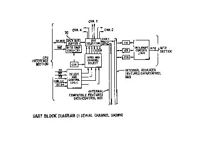
Referring to Fig. 1, the advanced register set A of
a Univer~al Asynchronous Receiver/Transmitter (UART) in
accordance with the present invention consist~ of eight
32-bit wide registers including five registers
(addresses ooooo through lO000) for standard serial
channel operation, DMA operation, and automated transmit
Tx flow control, one register (address lO100) for modem
or general purpose I/0 features and two register6
(addresse6 11000 and 11100) for external FIF0 control.
In addition to the advanced register set A, an
alternate register set B that includes eight 32-bit
register6 i6 accessible by setting an Alternate Register
Bit. The alternate regi~ter set B i~ used primarily
dur~ng U M T initialization. Received data comparison
registers, a baud rate divisor, and an I/0 data
direction regi~ter ~accessed at addressefi ~s indicated
in Fig. 1) ~re all accessible when the Alternate
Register ~it is set.
Referring to Fig. 2, five address pins A0-A4 are
u6ed to select the $nternal reg~sters. Identical
regi~t~r sets are present on e~ch of four gerial
chnnnels available in the UART embodiment described
below; ohannel select pins are provided for acce~s to
; the regi~ter 6et~ of each 6erial channel.
All four UART channels reset to a Compatibility
Mode. Two bits in a Compatibility Mode regi~ter set,
shown in FIg. 1, allow ~election of 8, 16, 32-bit bus
width or Compatibility Mode operation. These two bits
1 323706
g
are IER6 and IER7 in the Interrupt Enable Register
(IER), which is di~cussed in greater detail below. If
IER6,7 are cet to 00, 01, lo to 11, then the UART modes
are Compatibility, 8, 16, or 32-bit, respectively.
Referring again to Fig. 1, a DATA Register (addre~s
00000) i6 organized as 4, 2 or 1 byte wide fields,
depending on the programmed bus width. In Fig. 2, DATA
Register 10 represent6 the storage location at the top
of a FIF0, in the case of both the receiver and
transmltter portions of the UART, and i8 used to read
data from a Receiver RX FIF0 12 or write data to a
Tran~mitter Tx FIF0 14. (Any reference in the following
description to "Rx FIF0" or "Tx FIF0" is a reference to
internal UART FIFOs 12 and 14, respectively. Any
reference to an external Tx FIF0 or an external Rx FIFo
will be preceded by the word "external.")
The Rx and Tx FIFOs 12 and 14, respectively, are a
constant length regardless of the bus width. This means
that one-half the number of acce~ses are required to
transfer data to/from these FIF06 in the 16-bit mode as
compared to 8-bit mode and one-quarter the number of
accesses are required to transfer data to/from these
FIFOs ln 32-bit mode as compared to 8-bit mode.
As illustrated in Fig. 3, when transferring
multiple bytes from Rx FIF0 12 through A Data Bus Buffer
10 during a single access (16-bit or 32-bit Mode3, the
least significant byte on the CPU bus is the byte that
was received earlier than the other bytes; when
transferring ~ultiple bytes to Tx FIF0 14 through Data
Bus Bu~fer 10 during ~ single ~ccess (16-bit or 32-bit
Mode), the least sign~ficant byte on the CPU bus is the
first byte sent out on the serial line.
Byte Status Register (8SR) 16 provldes the
associnted l~ne ~tatu~ and byte match information for
each byte that the CPU reads from Rx FIF0 12. As shown
-lO- 1 323706
in Fig. 1, BSR 16 (address OoloO) contains 4, 2 or 1
byte-wide fields, depending on the programmed bus width.
The type of information provided by BSR 16 ~or each
received data byte i6 overrun, parity and framing
errors; break indication, byte match, and byte match ID.
Individual byte status remains in BSR 16 until the
associated data has been read from Rx FIF0 i2. ~SR 16
i~ updated with ~tatus for the next group of data bytes
a~ ~oon as these bytes can be read from the Rx FIFo 12.
lo In the block mode, described in greater detail below,
BSR 16 accu~ulates the status of each byte until it is
read. If there are fewer data bytes than the full bus
width to be given during the data read, the status bytes
in BSR 16 will correspond to the position of the data
bytes that can be read from Rx FIF0 12.
A Channel Status Register (CSR) provides the
status indication for all interrupts conditions. As
shown in Fig. 1, CSR ~addres~ 01000) contains two byte-
wide fields named Interrupt Identification (IIR) and
Bytes Till Exception (BTE) and two byte-wide reserved
fields.
The bits of the IIR field are set when their
associated interrupt condition is active. The
appropriate b~t in the IER must be set before any
indication in the IIR field can activate the external
interrupt signal. The IIR bit, however, is set when
there i8 an act~ve interrupt condition regardles~ of the
interrupt en~ble bit setting.
The following interrupt conditions each 6et one IIR
30 bit:
1. Reaching a programmed receiver trigger level
or an active receiver timeout condition sets
bit IIR7.
2. A match in any of the Comparison Registers
(described below) sets bit IIR6.
.. ....
1 323706
--11--
3. A line status error condition (parity,
framing, overrun, break) sets bit IIR5.
4. A change in any input status indicator from
the general purpose I/0 lines programmed as
inputs in the Data Direction Reg~ster
(described below) sets bit IIR4.
5. A match in either of the Comparison Tx Flow
Control Registers ~ets bit IIR3.
6. A Tx FIF0 Empty (TFE) condition or completing
a pre-programmed number of transmitter
transfers via DMA oet6 bit IIR2. The TFE
condition is cleared after the transmitter
enable bit is reset or a byte is loaded into
the Tx FIF0 14.
7. Completing a preprogrammed number of receiver
transfers via DMA sets bit IIRl.
IRR bit 0 (TEMT) is set when the transmitter is
completely empty. The setting of this bit cannot cause
an interrupt to occur, but it i~ included in this
register for the convenience of checking the transmitter
during half duplex operation.
Referring back to Fig. 2, in accordance with one
aspect of the present invention, Bytes Till Exception
Register (BTE) 18 indicates how many bytes remain in Rx
FIF0 12 until an exception i8 encountered. An
exception i8 defined in this context as anything other
than valid d~ta, e.g. an empty RX FIF0 12, a line status
error or a Comparison Register match. The BTE count is
the status indicator th~t the system will use most
often, since dat~ is usu~lly received by the UART
without error. The count in BTE 18 i8 updated a~ter
~very read of the RX FIF0 12 by the CPU.
BTE 18 elim~nates the need to check status on
every byte, since the CPU can now allow the UART to
perform this function. The UART then provides the count
1 323706
-12-
of consecutive valid data bytes from the top o~ the RX
FIFO 12 to the first exception. The CPU uses this
variable count to determine the number of bytes to
extract from the Rx FIF0 12 in a read access.
In the 16-bit mode, the Channel Status is accessed
through one 16-bit wide register; in the 8-bit mode, the
Channel Status is accessed through the two byte-wide
registers IIR and BTE.
Referring to Fig.l, Channel Exception Register
(CER) (address 01100) contains two byte-wide fields
named Interrupt Enable (IER) and FIFO Status (FSR) and
two byte wlde reserved fields.
The IER field holds the interrupt enable data. The
eight possible interrupts are:
1. Receiver FIF0 Trigger Level (RFT) or Receiver
Count (RCR);
2. Match (MCH);
3. Line Status (LSI);
4. Input Status (ISI);
5. Transmitter FIFO Flow Control (TFC):
6. Transmitter FIFO Empty (TFE) or Transmitter
Count (TCR); and
7. Receiver Timeout (RTO)
The RFT and RCR lnterrupts are mutually exclusive
operations in the UART, as are the TFE and TCR
interrupts. All interrupt priorities are user
determined.
The FSR field indicates the number of empty ~paces
ln Tx FIFO 14, whether or not there i6 ~ match or an
error detected anywhere in Rx FIFO 12, and which bytes
in the DATA Register are valid receiver serifil data.
Bits FSR7,6 indicate the number oS empty ~paces in Tx
FIF0 14 according to the following code:
FSR 7 6 Tx FIFO State
-13- 1 323706
0 empty
o 1 1/2 full
1 0 1 space empty
1 1 full
Bit FSR5 indicates that at least one byte iQ loaded
in Rx FIFO 12 that matches a byte in Comparison
Registers 2-7. This bit i8 used as an advanced signal
that there is a control ~haracter to be procecsed.
Bit FSR4 indicates that there is at least one Line
Statu~ indication associated with a data byte in Rx
FIFO 12. This bit is used as an advanced signal that an
error or break has occurred.
Bits FSR3-0 indicate the byte positions at the top
of RX FIFO 12 that contain valid data. This is needed
by the CPU only when there is less than an integral
number of data bytes presented during a 16- or 32-bit
wide read. When there are less bytes of valid receiver
data in DATA Register than the data bus i8 wide, then
bits FSR3-0 in the FSR field are set to indicate the
valid data byte positions. Only the consecutive data
bytes that are valid at the time that the FSR field is
read will be i~sued to the CPU during the next read of
DATA Register. Thus, by comparing the bits that are
set in the FSR to the bytes received from DATA Register,
the user can determine which bytes are valid. Thi8
technique means that the UART will not move additional
data into the top of the FIFO until the CPU reads the
DA~A register. Therefore, the CPU should re~d the DA~A
Register a6 800n as possible ~fter reading the FSR to
"free" any unused spacq in the top of the ~IFO. Bytes
will still be taken into the open space not included in
the top of the FIFG during this time.
Using a 32-bit wide CPU data bus, the following
example is given. The CPU reads the FSR field when
1 323706
-14-
there are ~nly three consecutive valid data bytes in Rx
FIFO 12 and no other data. Thu~, the FSR has the three
lowest order bits ~et. When the CPU then reads the DATA
Regi~ter, the UART will only issue three valid data
bytes in the lowest byte position~ and a 00 character in
the hi~hest byte position. Thi~ is the case even if a
valid data byte enters Rx FIFO 12 between t~.e time the
CPU reads the FSR field and the time it reads the DATA
Register. At all other times, the data presented to
the CPU bus will be a6 wide ~8 the bus.
Using a 16-bit wide CPV data bus, the following
example is given. The CPU reads the FSR field when
there is only one valid data byte in Rx FIFO 12 and no
other data. Thus, the FSR field has the lowest order
bit set. When the CPU then reads the DATA Register,
the UART will only issue one valid data byte in the
lowest byte positions and a 00 character in the highest
byte position. This i5 the case even if a valid data
byte enters Rx FIFO 12 between the time the CPU read the
FSR field and the time it read the DATA Regi6ter. At
all other times, the data presented to the CPU bu~ will
be as wide as the bus.
The Control Register (address 10000) i8 ths heart
of UART operations. It contains four byte-wide field6
that are identified in Figs. 1 and 2 as Channel Format
(CFR), Channel Operations (COR), Transmitter Operation
(TOR) and Receiver Operation (ROR).
The CFR field controls the UART block mode enable
and serial dat~ format. The block mode determine~
whether or not receiver ~rrors will be ~ccumulated in
BSR 16. If the block mode i8 enabled, BSR 16
~ccumulates all errors, breaks and matched information
~ssociated with data passing through the top of Rx FIFo
12. The results of this ~ccumulation i~ indicated by
the LSI and Hatch bits in the IIR field. After the CPU
~ 323706
-15-
reads BSR 16, all status bits are cleared, including the
associated IIR bits. Setting bit CFR6 enables the block
mode.
The serial data format specification includes data
length (5-8 bits), stop bits (1, 1-1/2, 2), and parity.
When bit CFR5 is o, one stop bit i8 ~ent with all data
combinations. When bit CFR5 is 1, two stop bits are
sent with all combinations of data, except 5-bit data
which i~ 6ent with 1.5 ~top bits. The setting of bit
CFR5 does not affect the receiver; it only checks for 1
stop bit. Bits CFR4,3 select the number of data bits
transmitted or received in each character. If bits
CF~4,3 are 00, 01, 10, or 11, then 5, 6, 7, or 8 bits
are seriallv transmitted and received, respectively.
Setting bit CFR2 enables parity transmission and
reception. When parity is enabled, even parity is
~elected by setting bit CFR1. Clearing bit CFRl when
parity is enabled results in odd parity. Setting bit
CFRO enables mark or space parity if the parity enable
bit CFR2 i5 set. If bits CFR2 and CFRO are set, then
CFRl determines whether mark (CFRl=O) or space (CFR1~1)
parity is tran6mitted and received.
Bit CFR7 is reserved. When written to, thi~ bit
should be set to O and when read it will always indicate
O.
The COR field controls Alternate Register
6electlon, receiver coupling, the data bu6 access width,
~MA mode selection, tran6mitter DMA enable and receiver
DMA enable. The Alternate Register6 (Baud Rate Divisor,
Alternate Function Register, ~ata Direction Register and
the Compari60n Register6 are accessible when bit COR7 is
~et. As 6tated above, the6e Alternate Regi6ters are
used primarily during initialization to establi~h the
ba6e hardware configuration of the serial channel.
1 323706
Two bits are used to determine the receiver
coupling (oo = normal, 01 = local loopback, lo = remote
loopba~k and 11 = echo mode). Selecting normal mode
(default) transfers all of the data the receiver
receives to Rx FIFO 12. Selectinq the local loopback
mode causes the data transferred to the transmitter to
be internally sent to the receiver. Selectinq the
remote loopback mode causes the transmitter to send
every byte the receiver receives, without these bytes
entering ~x FIFO 12. Selecting the Echo Mode causes the
transmitter to send ~ dupli~ate of every valid data byte
that is in the top of Rx FIFO 12. No bytes that cause
exceptions, i.e. an ISI condition or a Match condition)
are echoed. When the next byte to be echoed is a byte
with an except~on, Echo Mode is automatically disabled
by setting COR 6,5 to 00 (normal mode). At that point
in time, the CPU should respond to the exception and
echo the appropriate(s). The CPU will re-enable to ECHO
Mode after the exception is processed.
Using the Comparison Registers in con~unction with
the Echo Mode and Rx DMA only requires CPU intervention
during the receipt of control characters or corrupted
data. Because there are ~any control characters in the
ASCII set below lF hex that do not get echoed,
Comparison Register 2 has an additional capability. It
can match with any byte entering the ~x FIFO that is
le58 than or e~ual to its progra~med value when the
"less-than-or-equal-to" option is specified by setting
TOR5. When TOR5~0, Comparison Register 2 will operate
on an "equal-to" basi~ only. Thu~, in the case of
~utomatically echoing ASCII characters, the CPU can:
1. Set TOR5;
2. Load lF hex into CMP2;
3. LQad 7F hex into CMP3; and
4. Set COR 6,5 to 11, respectively.
, .,
1 323706
-17-
All characters received between the value 20 and 7E
hex will be automatically echoed by the UART. All other
value~ would create exceptions, thus signalling the cPu
and disabling the Echo Mode.
~its COR4,3 determine the data bus ~idth. The data
bus can be either 8, 16 or 32 bits wide. The 8-bit wide
bus has two modes of operation: Compatibility Mode or 8-
bit Node. If bits COR4,3 are equal to 00, 01, 10 or 11,
then the operating modes are Compatibil~ty ~ode, 8-bit
mode, 16-bit mode and 32-bit mode, respectively.
Bits COR2,1,o control Tx and Rx DMA. Bit COR2
determines the DMA mode; the two options are single-
transfer (bit COR2=0) and multi-transfer (bit COR2=1).
Setting bit CORl enables transmitter D~A; setting bit
CORO enables receiver DMA. When either of these options
are disabled, their output signals (DMA request) are
inactive (high).
The TOR field controls the transmitter and
Comparison Register operations. Through this byte, the
CPU can:
1. Enable or disable the transmitter:
2. Clear Tx FIFO 14;
3. Program a transmitSer break:
4. Enable transmitter control through /CTS;
5. Enable CMP2 to match on either a less than or
equal to condition:
6. Enable transmitter flow control through the
Comparison Registers;
7. Clsar the Compari~on Registers: and
The transmitter enable b~t allows the CRU to
oontrol the transmitter dir~ctly and also to override
any autom~tic ~low control changes that h~ve impacted
the transmitter enable state. Cle~ring Tx FIFO 14 is
useful if a retransmis~ion of data is required. The
transmitter break bit (TOR2~ sets the SOUT signal high
1 323706
-18-
for as long as iS equals 1. /CTS Tx flow control
enables or disables the transmitter as general purpose
I/O bit O changes from active to inactive, respectively.
Comparison Tx flow control enables or disables the
tran6mitter as Comparison Registerfi O and 1 match the
incoming data. These last two transmitter control
options automatically ~et and clear the transmitter
enable bit. As stated above, bit TOR5 enables the less-
than-or-equal-to option for Comparicon Register 2. If
TOR5=0, then CMP2 will match only when the byte entering
RX FIFo 12 equals its programmed value. If TOR5=1, then
CMP2 will match when ~he byte entering RxFIFO 12 is less
than or equal to its programmed value. Bit TOR6 enables
thP general purpose Comparison Registers (COMPo-7). Of
these registers, the one~ that are loaded with data
after a reset or A Comparison Register clear are the
one~ that are actually compared to the incoming data
bytes. TOR6 i6 used to clear the Comparison Registers
without resetting the UART; this bit i6 self-clearing.
This feature can be useful when loading the Comparison
Registers with a new set of data that contains fewer
byte~ than the previous set.
The ROR field control~ receiver Rx operations.
Through this byte, the user can control the insertion of
a flow control character into the tranfimitter data
~tream, the receiver clock source, the number of receive
character times delayed until a receiver timeout i~
is~ued, set-up the receiver trigger level and clear the
RX FIFO 12.
Writing to ROR7 causes the UART to insert the byte
programmed in Comparison Register 1 (i.e. XOFF) into Tx
Shift Register 20 a~ ~oon as the present character in Tx
Shi~t Register 20 has been sent.
The receiver clock ~RCLK) for each of the four
UART channels can be independently derived from any one
-19- 1 323706
of four sources. Setting bits ROR6,5 to 00, 01, 10 and
11 selects the RCLX source to equal the baud rate
generator ou~put, 1/2 the baud rate generator output,
1/4 the baud rate generator output or the signal at the
RCLK pin, respectively. After re et, the default value
of bits ROR6,5 is oo. These options are provided
primarily to allow high-speed transmission of data to a
peripheral device which will only be providing low-
speed keyboard or flow control data back to the CPU.
Secondarily, it requires fewer pins to support a UART
with multiple receivers. ~he transmitter is unaffected
by this selection and is always driven by the baud rate
generator output.
A receiver timeout interrupt is used by each serial
channel of the ~ART to indicate that data i8 present in
its Rx FIFO 12 and that no CPU or serial channel
activity has occurred during a specified period o~ time.
This feature activates when there is data in Rx FIFO 12
that can't reach the interrupt trigger level. It
ensure~ th~t the CPU will get an interrupt indicating
the presence of receiver data. The amount of delay
before a timeout interrupt i~ issued is programmable
using bit~ 4 and 3 of the ROR field. The delay is based
on the receiver cloc~ and is equal to an integral number
of receive oharacter times. If b~ts ROR4,3 are equal to
00, 01, 10 or 11, then the number of receiver character
tim~s delayed be~ore a timeout interrupt i8 issued is 1,
2, 3 or 4 receive ch~racter times, respectively. A
reminder timeout interrupt is i~sued i~ the following
conditions are met:
1. Data i~ in Rx FIFO 12;
2. The CPU has not accessea RX FIFO 12 during
the timeout period: and
3. No new serial number has entered RX FIFO 12
during the timeout period.
1 3237G6
-20-
The receiver timeout interrupt timer i5 reset whenever
a CPU access occurs or a byte i6 added to Rx FIFO 12.
It is ~tarted when there is a byte in RX FIFO 12.
Bit ROR2,1 determine the numher of bytes that
must be in RX FIFO 12 before a receiver interrupt is
is6ued. Setting bits ROR2,1 to 00, 01, 10, 11 will
result in a receiver interrupt being issued~when there
are 1, 4, 8 or ~.5 bytes, respectively, in Rx FIFO 12.
Clearing RX FIFO 12 i~ useful when there is an
error in the FIFO and it is not desired to extract each
byte individually before a retransmission occurs.
In 16-bit mode, the Control Register is accessed
through two 16-bit wide registers called the Channel and
the Tx/Rx Operation. In the 8-bit mode, the Control
Register is accessed through the four byte-wide
registers CFR, COR, TOR and ROR.
Referring to Figs. 1 and 2, the Channel I/O
register ~address 10100) controls all eight U~R~ I/O
pins that can be used for a modem interface or as
general purpose I/O. The modem interface is configured
automatically after reset and provides all of the
standard inputfi (/CTS, /DSR, /DCD, /RI) and outputs
(/RTS, /DTR). The Channel I/O register contains four
byte wide fields: Set I/O ~SIO), Clear I/O (COR), I/O
Registers (IOR), and Delta Input (DIR).
The Set I/O field is used to set individual output
pins. Corresponding output pins will be set on the
trailing edge of the write strobe when their bits in
this field have i8 written to them. These eight bits
are write only.
" The Clear I/O field is used to clear individual
output pins. Corresponding output pins will be cleared
on the tr~iling edge of the write strobe when their bits
in this field have ls written them. These eight bits
are write only.
1 3237Q6
-21-
Simultaneously writing to bits in both the set and
Clear I/o field~ that correspond to the same output pin
will result in no change in the output pin.
Simultaneously setting and clearing different output
pins through these fields i~ allowed. Setting or
clearing input pin~ only sets or clears the
corresponding output latch. ---
The IOR field determines the state of the out-going
I/O lines. ~riting a 1 to any of the IOR bits sets the
corresponding output pin high; writing a zero sets it
low. All writes to the IOR field are on ~ byte wide
ba~i~. If the corresponding pin is an input, the 1 is
written into the output latch, but it doesn't affect the
pin. Bits of this field are both read and write. When
reading bits that are designated outputs, the value of
the output latch is returned. Reading bits that are
designated inputs provides the status of the pins.
The DIR field provides input status information for
any of the I/O pins programmed as inputs (a change in
any of the input lines sets the corresponding bit in
this regi~ter). The setting of any delta bits in the
DIR field can cause an interrupt to be issued to the
CPU if ISI interrupts are enabled ln the IER field.
The~e status bits are read only; writing to them does
nothing. When the /CTS ~x Flow control bit in the DIR
field i6 enabled, I/O bit O i6 automatically made to
look like an lnput. The line becomes the /CTS input
line which enables ~nd disables the transmitter.
After re~et, the IOR, DIR and DDR fields are
~uto~atically initialized to a condition that a6sumes
the UART i~ connected to a modem or an Electronic
Indu6tries A660ciation (EIA) interface.
In t~i6 configuration, the bits are all programmed
to 1, a~6igned 6pecific functions (i.e., /CTS, /RTS,
etc.), and have a predetermined direction established in
1 323706
-22-
the DDR 220 Since this i5 essentially a general purpose
I/O port allowing various configurations, the default
pin and bit assignments are used when communicating with
a modem or an EIA interface to preserve sys~em
5 compatibility~ The default assignments for the bits are
as follows:
BIT IOR DIR DDR
O /CTS /CTS input
1 /DSR /DSR input
2 /RI /RI input
3 /DCD /DCD input
4 /RTS /CTS (delta) output
/DTR /DSR (delta) output
6 /GENR'L I/O /RI (delta) input
7 /GENR'L I/O /DCD (delta) input
The trailing edge of the /RI (ring indicator) signal
~ets the status bit in the DIR field.
In the 16-bit mode, the I/O Register is accessed
through two 16-bit wide registers called the Set/Clear
and the IOR/DIR Registers. In the 8-bit mode, the I/O
fields is accessed through the four byte-wide registers
SIO, CIO, IOR and DIR.
Referring to Figs. 1 and 2, the TCR and RCR
Registers 24 and 26, respectively, contain four byte
wide fields, three of which are named Tx Count (TCR) or
Rx Count (RCR), respectively. These registers, along
with the DMA capability of the UART, can be used to
create and control external FIFOs for the data, as
de~cribed in greater detail below.
The ~CR Register 24 (address 11000) i~ a
progra~mable counter used to track the number of bytes
loaded into Tx FIFO 14 via DMA. The number of bytes
th~t are to be transferred to Tx FIFQ 14 ViA DMA before
a TCR interrupt is issued by the UART is programmed.
The TCR counter 24 decrements ~or each byte transferred
to Tx FIFO 14. When the zero count is reached,
1 3~370~
-23-
transmitter DMAs are disabled and the TCR bit in the
IIR field is set. If the TCR bit in the IER field is
enabled, then the interrupt pin goeæ active low. If the
TCR bit in the IER field is not enabled, then only the
TCR bit in the IIR field is set. The actions
as~ociated with the TCR counter 24 only take place if
trænsmitter DMA is enabled and the counter 24 is loaded
with a value other than zero. If the TCR counter 24 is
not loaded ~fter reset, or is loaded with a value of
zero, then the actions ass~ciated with this counter do
not take place. This DMA process can be halted at any
time by disabling transmitter DMA or by loading counter
24 with zero.
The RCR register 26 ~address 111) is a
programmable counter used to track the number of bytes
loaded into system memory (RAM) via DMA. The number of
bytes that are to be transferred from Rx FIF0 12 via DMA
before receiver DMA ~nterrupt is generated by the UART
is programmed. The RCR counter 26 decrements for each
byte transferred from RX FIF0 12. When the zero count
18 reached, the UART disables receiver DMAs. The Rx DMA
bit in the IIR fizld i8 set and the UART's INTR line
goes active low if it i8 enabled in the IER ~ield. The
actions ~ssociated with counter 26 only take place if
receiver DMA i~ enabled and counter 26 is loaded with a
value other than zero. If the counter 26 i8 not loaded
after reset, or i6 loaded with a v~lue of zero, then the
actions associated with counter 26 do not take place.
Thi~ DMA proces6 can be halted at any time by disabling
receiver DMA or by loading oounter 26 w~th zero.
Referring again to Figs. 1 and 2, the Baud Rate
Divi~or Register (addres6 00000 in the Alternate
Register Set) contains two byte wide fields named High
Divisor (HDR) and LGW Divisor (LDR) and two byte wide
reserved fields. The HDR and LDR fields hold the 16-bit
1 323706
-24-
wide divisor for the channel's baud rate generator 24.
The HDR field contains the high byte of the divisor and
the LDR field contains the low byte. This register
resets to 000C hex. This i~ the divisor for 9609 baud
if XIN is connected to an 1.8432 MHz clock input.
The Initialization Register (address 00100 in the
Alternate Register Set) contains two byte-wide fields
named Alternate Function ~AFR) and Data Direction (DDR)
and two reserved fields. The AFR field contains three
~ctive bits. In accordance with a second aspect of the
present invention, setting bit AFR0 in any of the UART's
four channels allows the CPU to concurrently write to
the same selected register in each channel's register
set. This function reduces initialization time for all
of the common parameters that are loaded into each
channel's registers. The CPU can set or clear bit AF~0
by accessing any channel's register cet. When bit AFR0
i6 set, the channel select pins ~till determine which
channel will be accessed during read operations.
Setting or clearing bit AFR0 has no effect on read
operations.
Bit AFRl determines the function of the /MF pin.
If AFR1~0 (the default st2te), then the /~F pin will
provide the normal ring indicator function Ithe 6ignal
ring indicator is normally activated by a modem that has
sensed an incoming phone call.) When AFRl=l, the /MF
pin will provide the output for that channel'~ BAUDOUT
~ignal.
Setting bit AF~7 resets the associated channel.
30 This i~ ~ user reset that is channel specific, as
opposed to the reset that resets all of the channels.
The DDR field establishes the data direction for
the general purpose I/O. Setting Any bit to 1 in the
DDR field causes the corresponding I/O bit to be an
output. This field is always accessed on a byte wide
1 323706
-25-
basis. After reset, the DDR field is automatically
initialized to the default modem configuration. Th~ six
lower bit~ in the DDR field are used in the modem
interface and function as previously described, and the
two upper bits are programmed as inputs. The DDR field
rese~s to OC, which establishes the direction for he
~tandard modem and EI~ interface ~ignal assignments.
The Comparison Regi6ters (addresses 01000 and OllOo
in the Alternate Register Set) are byte-wide registers
that are compared to the bytes in RX FIFO 12 for a
match. Both register6 consist of four byte-wide fields
named Comparison O (CPo~ through Comparison 3 (CP3) and
Comparison 4 (CP4) through Comparison 7 (CP7). These
registers are programmed during initialization with the
data (typically, hex representation control characters)
that are to be matched during receiver operation. Once
they are enabled, by setting bit COR5, they will be
compared to the received data when it enters Rx FIFO 12.
Anytime a match with a received byte occurs, bit 6 in
the II~ field will be set when the matched byte is at
the top of Rx FIFO 12. An interrupt will be i~sued to
the CPU if it i~ enabled in the IER field. The Match
status bit in BSR 16 associated with the matched data
byte will be set, so that the matched byte can be
identified. Al60, the Comparison Register ID bits in
the appropriate BSR 16 will be set. Only Comparison
Registers that have been loaded by the CPU since the
last reset or since the activation of the Comparison
Register clear bit are compared to the received data
stream.
Flow control of the tr~nsmitted data stream can be
controlled by the UART directly. This is done by
programming Comparison Regi~ter O and 1 with flow start
~nd stop characters, respectively. When either of these
programmed start or stop flow control characters are
1 323706
-26-
matched in RX FIFO 12, the UART automatically enables or
disables the transmitter. The transmitter will complete
the sending of any byte in its Tx shift register 20 as
the flow control stops characters from being transferred
from Tx FIFO 14 to the shift register 20. These Flow
Control Co~parison Registers enable and disable the
transmitter by changing the state of the transmitter
enable bit. The flow control characters are received
on the SIN line to RX shift register 26 and can be 8
byte characters. The automatic flow control feature can
be overridden at any time by the CPU via the transmitter
enable bit. This feature can be disabled via the
automatic flow control bit to permit binary file
transfer. After reset, Comparison Registers O and l are
automatically loaded with the XON character (11 hex) and
the XOFF character (13 hex), respectively. If the
Comparison Flow Control bit is enabled, then the matched
characters are not put into RX FIFo 12 and the TFC
status bit in the IIR is set immediately. If the
Comparison Flow Control bit is not enabled, then the
matched characters are put into Rx FIFO 12 and when they
reach the top of FIFO 12, they cet the TFC status bit
in the IIR.
Automatic flow control is also available through
the /CTS pin. When enabled, this feature st~rts and
stops transfers to the Tx hift register 20 when /CTS is
active or inactive, respectively~ Transmitter flow
control via /CTS i8 accomplished by setting or clearing
the transm~tter enable bit. Transmitter ~low control
via both the Comparison Registers and /CTS i8 allowed.
If this iæ the cho~en node of oper~tion, then the most
recent input to the transmitter enable bit from the
Comparison Register~, the /CTS pin or the CPU prevails.
In 16-bit mode, the Comparison Registers are
1 323706
-27-
accessed two at a time. In 8-bit mode, the Comparison
Registers are accessed one at a time.
Each of the four serial channels of the UART can
control both internal and external FIFOs for the UART
transmitter. The internal Tx FIFO 14 for each channrl
i5 16 bytes deep. Based on 24-bit wide registers, the
external Tx FIFOs can be up to 16.777216 Mbytes deep.
In an internal Tx FIFO transfer, the CPU writes
data to Tx FIFO 14 in bus wide groups. As stated
above, the data is sent out serially by the transmitter
with the least significant byte sent first. The
transmitter sends all data in Tx FIFO 14 as long as Tx
FIFO 14 is enabled. If Tx FIFO 14 is disabled while a
byte is being shifted out, that particular byte is
finished, but no more bytes are transferred to the ~x
shift register 20.
If the number of data bytes to be transferred to
Tx FIFO 14 is less than one bus width, the CPU will
send advanced notice to the UART. As stated above, this
is done by activating the /HBE and A0 input signals.
Data in the Tx FIFO 14 is always stored in consecutive
byte locations regardless of the number of bytes in each
CPU transfer.
The CPU ~ust program bits 2 and 1 of the Channel
Operation Register (COR2,1) for DMA mode and Tx DMA
enable, respectively. Transfers to Tx FIFO 14 executed
by DMA are ~tarted when Tx FIFO 14 i5 empty. In DMA
mode 0, the transfer reguest pin deactivate~ after the
first transfer of data into TX FIFO 14. In DMA mode 1,
the transfer request pin deactivates when Tx FIFO 14 i6
full. All transmitter DMA data transfers must be the
full width of the bus or the /HBE and AO bus signals
~ust indicate a byte-wide transfer.
The UART also provides for maintaining an external
Tx FIFO in conjunction with a system DMA unit. This is
~ 323706
-28-
done to allow increased transmitter FIFO length without
significantly increasing UART die size.
Referring to Fig. 7, to maintain an external Tx
FIFO, DM~ control circuitry requests DMA transfers and
notifies the CPU when a preselected number of bytes are
to be transferred from the system memory via DMA. One
additional regi6ter i6 provided for external FIFO
control. This is the Tx DMA counter regi~ter. It keeps
track of the number of byte~ transferred from the memory
via DMA. The CPU programs thi6 counter with the number
of bytes to be transferred. The counter decrements for
each byte transferred during Tx DMA. When the counter
reaches 0, the Tx counter bit in the IIR field is set
and further TX DMA requests are automatically disabled
by clearing the Tx DMA enable bit (CORl). If enabled,
i.e., bit IER2 set, an interrupt will be sent to the
CPU. The CPU responds to this interrupt by:
l. Checking the CSR to determine the interrupt;
2. Checking the Tx DNA counter to disable the
interrupt;
3. Restarting the ~ystem DMA for another Tx
transfer; and
4. Setting the Tx DMA enable bit (CORl) to
continue further Tx DMA requests by the UART.
The TX DMA counter 24 will be automatically
reloaded after the Tx DMA enable bit is set. The CPU
may reprogram the DMA counter 24 at anytime. If the DMA
counter 24 18 reprogrammed to O, or if it i8 not
progra~med after a reset, then the external FIFO control
i5 not active.
1~ the number of bytes to be transferred via TX ~NA
is les6 than an integral number of bus widths, one of
two options is available.
1. If the system DMA is sophisticated enough to
recognize and signal the less-than-bus-wide
1 323706
-29-
transfer of data to the UART, then it can
execute the transfer itself through /HBE and
A0 inputs;
2. If the DMA can't execute this transfer, then
the CPU must do the last transfer.
Each serial channel of the UART can also control
internal and external FIFOs for the receiver. The
internal ~x FIFO 12 for each channel i5 16 bytes deep.
External RX FIFOs can be up to 16.777216 Mbytes deep.
In an ~x FIFO transfer without DMA, bits 2 and 1 in
the ROR field are set to determine the number of bits in
the RX FIFO 12 before an interrupt is triggered (00=1
char., 01~1/4 full, 10=1/2 full, 11=7/8 full). Setting
bit 7 in the IER field allows an interrupt to be issued
when Rx FIFO 12 fills to the predetermined trigger
level. Bits 4 and 3 of the ROR field determine the
duration, expressed in character times, that a data byte
must wait in Rx FIFO 12 until a timeout interrupt is
issued to the CPU. This interrupt, if enabled, is
issued if at least one data byte has been in Rx FIFO 12
for the number of character times specified and there
has been no CPU access or serial data entering Rx FIFO
12 during that time. Setting bit IER1 enables timeout
interrupts.
The CPU, upon receiving an interrupt will read the
IIR field and check each bit for a pending interrupt.
Finding bit 7 set indicates that Rx FIFO 12 is at its
trigger level or a timeout interrupt is pending. The
CPU reads the Bytes Till Exception Register (BTE) 18 to
get the count of the number of valid bytes it can remove
from Rx FIFO 12. Then ~t reads these bytes from the
DATA Regi~ter until that count is reached.
Since the CPU data bus can be wider than one byte
and the serial data is always received in one byte
increments, it is possible to have fewer bytes in Rx
t 323706
-30-
FIFO 12 than the bus is wide. This possibility will
only occur during the last access by the CP~ before the
count of BTE 18 reaches zero. For example, if the data
bus is 2 bytes wide and there are 15 bytes to be removed
from Rx FIFO 12, as indicated by ~TE 18, the CPU can do
seven consecutive 2 byte wide reads without any further
need to check the data status. Before the last read of
the DATA Register, the CPU reads the FSR field to
obtain the valid byte positions. It then reads the DATA
Register for the last time to extract the remaining
data bytes.
If another byte enters Rx FIFO 12 after the CPU
has read the FSR field, but before it has read the DATA
Register, the new byte will not be placed at the top of
Rx FIFO 12. It is not added to the data that the CPU
could read from Rx FIFO 12 until after the read of the
DATA Register is finished.
DMA transfers using only RX FIFO 12 are prepared
for by executing the following initialization steps.
The RX FIFO trigger level bits in the ROR field (ROR3,2)
and the timeout delay bits ROR5,4 are set to the
required level. The Rx DMA mode select bit (COR2) i6
programmed for either single or multiple DMA transfers
~0 and 1, respectively). Assum~ng DMA mode 1 is
selected and RX DMA enabled ~COR 2,0 6et), the following
occurs.
Automatic DMA reguests to transfer data from the
UART will begin whenever the data reaches the trigger
level. All consecutive valid data will be transferred
until either an exception is encountered or unt~l the
number of valid data bytes left is less than one bus
width. If the first exception encountered is an empty
Rx FIPO 12, DMA requests will stop until the trigger
level i8 reached.
-31- 1 323706
If the first exception is a line status error, DMA
transfers will stop when this byte is among those to be
transferred next. The appropriate line status error
bit(s) will be set in the IIR field and ln BSR 160 If
enabled, an interrupt will be issued to the CPU. At
this point, the CPU responds as follows:
1. Read the CSR field to determine the type of
interrupt(s~;
2. Read the FSR field to determine the position
of valid data;
3~ Read BSR 16 to pinpoint the 6pecific nature of
the exception and clear the interrupt(s);
4. Execute the service routine for the specific
~SI; and
5. Clear Rx FIFo 12 and execute the purge routine
to eliminate the remaining incoming data
associated with that block, then request
retransmission of the data.
Automa~ic R~ DMA transfers will aga1n start after
the trigger level is reached or a timeout occurs.
If the first exception is a Comparison Register
Match, the appropriate bits in the IIR field and BSR 16
will be set. If enabled, an interrupt will be iscued
to the CPU. At this point, the CPU responds as follows:
1. Read the CSR field to determine the type of
interrupt ~8)
2. Read the FSR field to determine the valid data
byte locations;
3. Read BSR 16 to identify the matched bytes;
4. Read the Data Regi~ter, discarding the matched
bytes and keeping the data bytes; ~nd
5. Execute the appropriate control character
service routine.
If the number of consecutive valid data bytes at
3~ the top of Rx FIFO 12 is less than one data bus width
.....
-- 1 323706
-32-
wide (e.g., 3, 2, or 1 byte in 32-bit access mode; 1 in
16-bit access mode), then DMA requests will stop and the
UART will wait for enough bytes to arrive to reach the
trigger level or until a timeout occurs. If a timeout
occurs, the CPU will be required to remove the remaining
valid data bytes and set the RX DNA enable bit to
restart the Rx DMA requ~sts. Procedures for handling
less than a data bus width of data are as follows:
1. Check the CSR field to determine the interrupt
and consecutive valid data;
2. Read Rx FIFO 12 to extract all remaining bytes
(check the FSR field when appropriate);
3. Prepare system DKA for next transfer; and
4. Set the Rx DMA enable bit to allow DMA
transfers to continue.
DMA mode O operation is handled in the same way as
mode 1, except that ~MA requests are started as soon as
one data bus width of valid data (4 bytes in 32 bit
mode, 2 in 16 bit mode) has been accumulated.
Automatic DMA request stops for any exceptions mentioned
for DMA mode 1. DMA transfers will restart (according
to mode O criterion) after any exceptions, timeouts or
insufficient valid data width conditlons have been
cleared and the Rx DMA enable bit i8 set.
The UART also provides for maintaining an external
Rx FIFO in con~unction with a system DMA unit. This is
done to allow incr~ased Rx FIFO length without
6~gnificantly increasing the UART die size. Referring
to Fig. 8, to do thi~, control circuitry that requests
DMA tran6fers and notifies the CPU when a preselected
number of bytes has been transferred is provided. One
additional register i8 provided for external RX FIFO
control. This is the Rx CNT count register 26. It
keeps track of the number of bytes transferred from Rx
FIFO 12 via DMA. The CPU programs this counter with
~ 32370~)
-33-
the number of bytes to be transferred. The counter
decrements with each valid byte transferred. When it
reaches 0, the Rx CNT bit in the IIR field is set and if
enabled (IER7 set) an interrupt is issued. The Rx DMA
bit in the control register (COR0) is cleared at this
time, disabling further RX DMA. UART operation reverts
to the non-DMA transfer mode until the CPU sets the Rx
DMA enable bit, again. The CPU responds to the RX CNT
interrupt by:
1. Reading the CSR field to determine the
interrupt;
2. Reading the Rx CNT register the clear the
interrupt;
3. Processing the bytes stored in the external Rx
FIFO;
4. Preparing the system DMA for subsequent
transfers; and
5. Setting the RX DMA enable bit in the Channel
Operation register to allow subsequent DMA
transfers.
In mode 1, DMA reaching trigger level of RX FIFO 12
starts the transfer to the external RX FIFO. The
transfer continues until all consecutive valid data
bytes in Rx FIFO 12 have been transferred, there is a
line status condition or until a byte match condition
occurs at the top of Rx FIFO 12. If the counter is not
zero and there is less than one bus width of
consecutive valid data at the top of RX FIFO 12, then
the UART will wait for enough bytes to arrive to reach
the trigger level ~nd continue a full bus width DMA
transfer. If enough bytes don't, arrive a ti~eout
interrupt will be issued to the CPU. ~he CPU response
to a timeout interrupt is:
1. Check the CSR field, to determine the
interrupt and consecutive valid data;
1 323706
-34-
2. Check the RCR to clear the interrupt and
determine the number of bytes in the external
Rx FIFO that need to be proce~sed;
3. Read Rx FIF0 12 to extract all remaining bytes
(check the FSR field when appropriate);
4. Process the bytes stored in the external Rx
FIFo; and
5. Start a routine to handle the remaining
incoming bytes in this block.
The RX DMA counter 26 is reloaded to the
preprogrammed value after the RX DMA enable bit is set.
The enabled Rx DMA transfer will start again, as soon
as, the trigger level is reached. In DMA mode 0,
transfer will start, as soon as enough data is assembled
to make one complete bus width transfer.
The CPU may reprogram the DMA counter at anytime.
If the DMA counter i8 reprogrammed to 0 or it is not
programmed after a chip reset, then external RX FIFo
control is not active. Line status or byte match
conditions are handled the same way as in the internal
Rx FIF0 mode.
There are eight types of interrupts the CPU can
enable via the IER field. Two report receiver status,
three report transmitter ~tatus and the other three
report input ~tatus, line status and comparison register
matches.
Setting bit IER7 allows an RX FIF0 12 at trigger
level lndication (IIR7) to activate the interrupt. If
this interrupt is pending, the CPV response is:
1. Check the IIR field to deter~ine the
interrUpt:
2. Check the Bytes Till Exception Register 4 to
determine the number of bytes till an
exception;
_35_ ~ 3 2 3 7 0 6
3. Extract all of the consecutive valid data
bytes till an exception (bit IIR7 is cleared
when the data falls below the trigger levels);
and
4. Read the FSR and BSR fields and extract any
remainin~ valid data bytes along with any
pertinent line status or match information
about the invalid data bytes.
Setting bit IER7 when the external RX FIFOs are in
use allows the RCR (IIR1) indication to activate the
interrupt ~ignal. The RcR indication IIR1 is 6et when
the RCR reaches 0.
Another Rx interrupt enabled by setting bit IE~1 is
the timeout interrupt. This indication goes active when
an internal timer reaches zero. The indication means
that data has been sitting in Rx FIFO 12 longer than a
preprogrammed limit without the CPU taking action or
additional data srriving. This timeout interrupt
prevents data that can't reach the trigger level from
ZO being stuck in the FIFO indefinitely. It trigqers the
same indication (IIR7) as RFT, because the CPU response
is the same for timeout, as for the RFT indication.
The internal $imer for timeout indication is
started when the first byte enters Rx FIFO 12 And is
stopped when the last byte is removed from Rx FIFO 12.
The timer is automatically restarted each time the CPU
removes a byte from Rx FIFO 12 or each time the Rx shift
register 27 loads a byte 27 from Rx FIFO 12 or each
time RX 6hift reg~ster loads a byte into it. The
duration of the timer is program~ed by setting bits 4
~nd 3 in the ROX. All timer durations are increments
of 1 character time (00=1 char., 01-2 chars., 1 ~ 3
chars., 1~4 char6.). If the programmed duration of the
timer expires before the CPU accesses Rx FIFO 12 or
~,
1 32370h
-36-
another retrieved byte is loaded into Rx FIF0 12, then
the timeout indication (IIR7) is set.
An external RX FIFO is considered to be in use when
both the RX D~A enable bit is set and the RCR 26 is
loaded. The RX timeout operation when using an external
~x FIFO is identical to that listed above f~r RX FIFO
12, except in two respects.
1. The timeout duration is lengthened by 100x.
This is done because it is assumed that the
system will be receiving files instead of
accepting input from a user terminal and,
therefore, the timeout durations should be
much longer. Specifi¢ally, if the file is
being transferred at 9600 baud ~sing ~ data, 1
stop and no parity, then the Rx timeout delays
available to the user are approximately 100,
200 300, 400 ms.
2. Once ~tarted, the timeout timer is only
disabled if both Rx FIFO 12 is empty and RCR
26 ~ 0. This allows the timer to monitor time
delays for both the internal and external ~x
FIF0s. This is useful because data could
conceivably be stuck in either internal,
external or both Rx FIFOs.
Setting bit IER6 allows the Comparison Register
~atch indication to issue an interrupt. The comparison
match will occur when the Comparison Register enable bit
TOR6 i8 set and a data byte at the top of Rx FIFO 12
matches a byte loaded into a Comparison Reqister. In
recponse to the interrupt, the CPU will:
1. Read the IIR field to determine the interrupt;
2. Read the FSR field to determine if there is
valid data at tbe top of Rx FIFO 12;
3. Read BSR 16 to determine the byte that matched
1 3237~
-37-
and what it was (this clears the interrupt);
and
4. Read the DATA Register.
Setting bit IER5 allows Line Status indications
(LSI) to activate an interrupt when the bytes come to
the top of Rx FIFO 12. These occur due to either an
overrun error (OE), parity error (PE), framing error
(FE) or a break indication (BI). The specific
indication i6 associated with the byte that caused it in
BSR 16. However, the OE will be indicated as ~oon as
the UART recognizes this condition. In response to an
LSI, the CPU will:
l. Check the IIR field to determine the
interrupt;
lS 2. Check the FSR field to determine if there is
valid data at the top of Rx FIFO 12;
3. Check BSR 16 to determine the byte(s) that
caused the LSI (this clears the interrupt);
and
4. Read Data Register 10.
Settinq bit IER4 allows the Input Status Indication
(ISI) to activate an interrupt. An ISI occur6 when any
of the general-purpose input lines change. If bit IER4
is fiet then this indication will activate an interrupt.
The CPU response to this interrupt is:
1. Read the IIR field to determine the interrupt;
and
2. Read the DIR field (this clears the
interrupt).
Setting bit IER3 allows the Tx flow control
" indication (TFC) to activate an interrupt. The TFC
indication occurs when a change to the Tx enable bit has
been made due to a match in Rx FIFO 12 with Comparison
Register Q or 1 or due to a change on the /CTS pin.
This assumes that these flow control options are
1 ~3~06
-38-
enabled. The Tx flow control consist~ of automatically
starting or stopping the transmitter when user
determined bytes ~uch as XON or XOFF are detected in the
data stream. Reading the TOR field to check the Tx
enable state clears the interrupt. It's purpose is to
inform the CPU that a change of state has occurred to
the Tx enable bit. The CPU can override an automatic
setting of the Tx enable bit at anytime by simply
writing to it. This interrupt occurs immediately upon a
match if TOR3 i~ set. I~ TOR3 is O and a match occurs,
then the interrupt goes active when the flow control
character reaches the top of the F~FO. If TOR3 is set,
then the flow control characters are not put into the
FIFO.
Setting bit IER2 allows the Tx FIFO empty
indication or the Tx DMA count = O indication to
activate an interrupt. When Tx FIFO 14 is empty, an
indication is given through bit IIR2. The CPU responds
to this interrupt by:
1. Reading the IIR field to determine the
interrupt: and
2. Fither loading data into Tx FIFO 14 or if its
the start of TX DMA, enabling the Tx DMA bit
~this clears the interrupt). If there is no
data to transmit the CPU can clear the Tx
enable bit to clear the interrupt.
If an external Tx FIFO i8 in use, then the IIR2
indication i8 activated when the Tx DMA counter reaches
it6 0 count.
Once the Comparison Registers have been programmed
and enabled, each byte entering Rx FIFO 12 i8 checked
for a match. The UART contains 8 Comparison ~egisters
and only those that are explicitly loaded by the CPU are
actively compared. Therefore, any number of "control"
characters up to 8 can be in use. A match with any
~ 3~3~,~6
-39-
Comparison Register, except Comparison Registers 0 and
1, will be indicated by bit IIR6 and the appropriate BSR
bits when it is among the next data to be taken from the
top of Rx FIF0 12. Assuming an active interrupt was
caused by a Comparison Register match, the CPU will:
1. Read the IIR field to determine the interrupt;
2. Read the FSR field to determine the-~valid data
at the top of RX FIF0 12:
3. Read BSR 16 to determine which byte matched
and what it was; and
4. Read Data Register 10 to extract the bytes
from the Rx FIFo 12.
The CPU retrieves the valid data sorting it from the
control character(s~. A match with the Comparison
Registers handling flow control (0 and 1) is indicated
by IIR3.
Transferring byte-wide serial data to a word-wide
(i.e. 16-bit) parallel data bus and vice versa requires
an additional constraint that is not present memorv/CPU
exchanges. In theorv, the CPU may access each serial
channel any one of three ways: odd byte, even byte or
word transfers. Because the data from each channel is
always ordered byte-by-byte, it must be presented to the
CPU with the original order preserved. Two signals
issued by the CPU typically control the way in which the
data will be transferred. The /HBE and A0 input signals
to the UART, which are used to control byte transfer6
ind~cate the number of bytes and which part of tbe 16-
bit CPU bus is used, not which byte6 in the UART FIFOs
will be acce~sed.
The following describe~ typical 16-bit bus
transfers to a peripheral and then the 16-bit bus
transfers to the UART.
As stated above, a 16-bit wide data bus allows the
CPU to transfer data to or from a peripheral device in
1 323706
-4~-
three different ways. ~able 1 ~elow sets forth the
manner in which the UART will enable the data bus for
the given st~tes of /HBE and Ao. During conventional
transfers, the CPU establishes the cvntrol signals /HBE
S and A0 and transfers the data utilizing normal transfer
procedures. The data, if it i being sent, has a
predetermined location to go to based upon t~e address
and the data position on the data bus. This is true
for each of the three types of transfers. If the data
lo is being received by the cPu~ then it i~ also handled in
the CPu based upon the address and the data's position
on the data bus.
When simultaneously transferring from the CPU to
the UART 16 bits of data that is to be transmitted
serially, the data's predetermined position in the VART
FIF0 depends upon the address and the data bytes'
position on the data bus. ~owever if only 8 bits of
data is being sent to the UART for serial transmission,
then the predetermined position in the UART's FIF0
depends upon the address and the number of bytes being
sent, not by the byte's position on the data bus.
When the transferred data has been received
serially by the UART and will be transferred across a
16-bit bus to the CPU, the data's "order of reception"
must be preserved during the 16-bit data bus transfer.
During a 16-bit wide data transfer, this order is
pre~erved with conventional csnstraints of address and
data bus position. However, during an 8-blt transfer,
the next byte available in the UART FIF0 is transferred
to the dat~ bus regardless of the position on that bus
that it will occupy, in other woxds~ regardless of
whether it will be in the high ~yte or low byte
po~ition.
1 323706
--41--
TABLE 1
TRAI~SFER TYPE /HBE AO BUS ACTIVITY
even word 0 0 D15-Do
odd byte 0 1 Dl5-D8
even byte l 0 D7-D0
As stated above, the odd and even byte transfers
determine on which part of the bus the next byte in the
RX FIFO 12 will be placed. The Data and Status
Registers operate in the same ~anner. Status must be
read before data in order to associate the status byte
with the appropriate data byte.
Writing to the DATA Register loads data into Tx
FIFO 14. Data can be written to the DATA Register using
any /HBE and A0 combination. During single byte
transfers, the data byte will be located in the next
available space in Tx FIFO 14, regardless of its
position on the CPU bus (D15-D8 or D7-D0). Word wide
data i8 loaded into Tx FIFO 14 assuming that the data
byte on D7-D0 should be transmitted immediately before
the data on D15-D8.
All other registers besides Data and Status can be
addressed on a byte-by-byte basis using /H~E and A0.
For example, in the 16-bit acce6s mode, if the register
at address 5 is accessed with /~BE~0 and A0=l, then the
register contents will be placed on D15-D8. Writes to
odd and even byte wide registers are accomplished in a
similar way using these strobes, as are word wide
strobes.
It should be understood that various alternatives
" to the embodiment described herein may be employed in
practicing the present invention. It is intended that
the following claims define the invention and that
methods and structures within the scope of these claims
and their equivalents be covered thereby.