Note : Les descriptions sont présentées dans la langue officielle dans laquelle elles ont été soumises.
.~ ~
3~3~2
b~:~
r~ti~ oLæt~ ~ lc ~av~
d~ic ard in pr1~ r to ~t~r~o~ t~ ~d
S ~e~optl~ laat~rla~, ~ D lithlma a~bat~ (a~B)
and xrP~ hav~ rofractl~ ln~os ~i~ Yar~ ac~rdlDg to
the ~ itude ~d dlre~ion of appll~d Ql~trlc ~leld.
ha~guiàe d~ es ba8~ on s~ch ~ rlal~ ar~ potentlal~y
use~ul ~or opti~ ~lbr~ co~u~l~tion a~d 81gllal
proc@~slnq sy~te~ yplcall~ ~uch dsvlce~ req~lred
to op~rate ll~th llght of ~aYel~D1~18 11~1 the range 0.6 to
1.6~a, and ~ partieular ~ith light ln the range 1.3 to
1.6~.
There are tvo ba81~: deYiCe typ88s dlrectlo~al
coupl~r~; and ~a~h-Z~der ~ ~t~r~ero~eters. ~he
flrsl: o~ these utlllse~ ~e ~lectro~ ffect to
~orltrol ~h~ coupllng bet~ a palr of ad~a~e~t
~sav~guide~ t~oll~g tbeir r~fractiY~ indi~e~ lt i~
po~sible to ~ouple llqbt ~ro8l o~e s~veguide to the other
or 7ice ~ersa. I~ a~ ~ interf~roaeter a~ ~put ~aveyuide
i~ ~oupled l~ o~tput ~avegulde b~ a pair of ~a~egQide
ar~u 8ach a~ ha3 a~ a~s~:iate3 el~trode h~ ~eans of
whi~h it i~ lble to ~o~trol ~ rsfra~c~e i~dices of,
and hence the ~el~ity o~ propaqatlon in, the t~ ar~
2s indep~ndently. It 1~ t~erefore po~sible, by co~rolli~g
the appli~d electri~ field~, to produ~e phase dlfferences
bet~een ~gnals travelling i~ the t~o ar~ resulting i~
constructive or destructlve inter~erance ~rhen th~y are
combined. Th~s it is po85ible to a~plitude ~odula~ ~put
opti~al ~iqnalB a~cording to the ~ol~age dlf~srence
bet~een the ~lectrode~.
~'
~!
.
'
~ ' ' " ' ~ '
~ 323~
-- 2 --
Unfortunately, materials such as LNB, which exhibit
the electro op~ic effect tend also to be pyroelectric:
electric fields are produced within the material as the
result of a temperature change. With some materials,
notably Z cut LNB, the pyroelectric effect is so strong
that a temperature change of a degree or less may be
sufficient ~o produce an electric field comparable to that
applied to produce switching o~ state~ ln a directional
coupler or N$ interferometer made of the material. Such
o electric fields strongly affect the optical states of the
devices. Consequently it is necessary, with materials
such as Z-cut LNB which exhibit a strong pyroelectric
effect, to provide very precise temperature control if
reliable and repeatable perorman~e is to be achieved ~rom
electro-optic waveguide devices based on such mater~als.
However, even with good control of environmental
temperature effects, thermally-induced instabllities may
remain in devices in which there is power dissipation in
the electrodes.
Examples of device~ with power dissipating electrodes
include directional couplers and NZ interferometers having
travelling-wave electrodes. The use of travelling-wave
electrodes potentially enables the production of devices
capable of very high speed operation (typically switchable
at gigabi~ rates). A further advantage of such devices is
that they offer a very large bandwidth, typically from dc
to 4GHz.
Because the travelling-wave electrode is part of a
transmission line and has finite resistance, non-zero
signal levels cause power to be dissipated in the
electrode, thus raising the temperature of the underlying
waveguide. The stahility of these devices is jeopardised
if there is in the electrical signal applied to the
electrodes a low frequency component having a period
.
, ' ~ ~ ' ''
;
.323~
longer than the thermal response time of the electrodes
(of the order of o.l second) as such components cause
S variations in power dissipation and hence temperature
fluctuations. This power variation can shift the transfer
characteristic by as much as 3 volts or mora which, the
switching voltage being in the range 3.5 to 4.0 volts,
makes the device unusable.
One solution to this proble~ which has been
proposed is to decouple the travelling-wave electrode by
inserting a capacitor (e.g. 47nF) between the travelling-
wave electrode and the transmission line termination to
remove the dc component of the switching voltage. The
capacitor is of course transparent at very high
fre~uencies and therefore does not inhibit performance at
such frequencies. At low frequencies the capacitor limits
the charge passed by the travelling-wave electrode,
limiting the power dissipation in both switching states
and hence limiting temperature fluctuations. ~he
disadvantage of this arrangement is that, in practice, the
full bandwidth of the device will not be available, the
device typically being unusable at switching frequencies
in the range lMHz to 200MHzo As a result the device user
2s has to choose to operate the device from dc to a few MHz
or from a few hundred MHz to 4GHz.
It is an object of the present invention to
provide a biasing arrangement which largely avoids the
previously mentioned problems and disadvantages.
According to the present invention there is
provided a method of driving an electro-optic device
having a power dissipating electrode structure comprising
an electrode and a ground plane electrode, the device
being switchable between first and second distinct states
by application of respective first and second potentials
to the power dissipating electrode, characterized in that
a bias voltage is applied to the ground plane electrode
,~ ~
~.
:
,
.
~23~20
- 4 -
such that the magnitude of the current carried by the
power dissipating electrode is substantially the same in
S each of the first and second states.
In accordance with an embodiment o~ the
inv~ntion, apparatus comprising an electro-optic device
having a travelling wave electrode structure includes a
travelling wave electrode and a ground plane electrode,
the device bein~ switchable between first and second
distinct states by the application o~ respective first and
second potPntials to the travelling wave electrode; and
apparatus for supplying the first and second potentials to
the travelling wave electrode, the apparatus further
comprises apparatus to bias the ground plane electrode
such that the first and second potentials are of
substantially equal magnitude but of opposite sign.
In accordance with another embodiment, a method
of driving an electro-optic waveguide device having a
travelling wave electrode structure includes a travelling
wave electrode and a ground-plane electrode, wherein a
bias voltage is applied to the ground-plane electrode to
enable the use of substantially equal travelling wave
electrode potentials of opposite polarity in switching by
a full switching voltage V~ to or from a phase bias point.
In accordance with another embodiment, an
apparatus comprising an electro-optic waveguide device
having a waveguiding region formed in a pyroelectric
material, and a travelling wave elactrode structure which
includes a travelling wave electrode and a ground plane
electrode, the device being switchable between first and
second distinct states by the application of respective
first and second potentials to the travelling wave
electrode; and apparatus for supplying the first and
second potential~ to the travelling wave electrode, the
apparatus further comprises apparatus to bias the ground
plane electrode such that the first and second potentials
are of substantially equal magnitude but of opposite sign.
. -
..
'
! ~323s2a
- 4a ~
Praf~rred embodiments of tha present invention
will now be described, by way of example only, with
S reference to the accompanying drawings in which:
Figure 1 is a schematic plan view of a
conventional Mach-Zehnder interferometer having a
travelling-wave electrode structure and its driving
circuitry;
o Figure 2 shows the transfer characteristic of an
interferometer such as that shown in Figure l;
Figure 3 is a schPmatic plan view of the
interferometer of Figure 1 modified according to the
invention;
Figure 4 shows the transfer characteristic of
the interferometer of Figure 3 opexated according to the
invention.
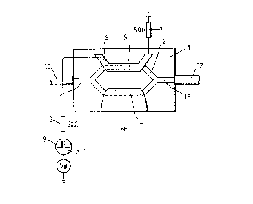
In Figure 1 a typical travelling~wave electrode
Mach-Zehnder interferometer is shown. The device is
formed on a Z-cut lithium niobate (LNB) substrate 1,
typically 40mm long, lOmm wide and lmm thick, and
comprises a waveguide structure 2 formed by diffusing
titanium into the LNB. A ground plane electrode overlies
one of the interferometer arms 4 and is connected directly
~S to ground. Over the other interferometer arm 5 there
extends a travelling-wave electrode 6. One end of the
travelling-wave electrode 6 is connected via a 500hm
transmission line termination 7 to ground. The other end
of the travelling-wave electrode is connected via a 5~ohm
transmission line 8 to the modulating voltage source 9 the
other pole of which is connected to ground. Optical input
signals are supplied to the interferometer by an optical
" .
;~.
~ 3 2 i3 ~
fibre 10 which is aligned with the ~aveguide input
portion 11. The inter~erometer output is fed into a
second optical fibre 12 aligned with the waveguide output
portion 13.
Figure 2 shows the transfer function of an
interferometer such as that shown in Figure 1. The
transfer function i9 essentially of periodic co~ squared
type. For full modulation, the electrode potential (that
is the potential dlfference between the travelllng-wave
electrode and ground potential) is ~witched so that the
light output is switched between a peak and a trough or
YiCe versa. The elec~rode voltage required to drive the
output from a peak to a trough is called the switching
voltage V~. a typical switching voltage for 20~m long
electrodes on Z-cut LNB is about 3.5V. The curve
represented as a broken line corrasponds to a typical
transfer characteristic, ~here the light output null
corresponds to a non-zero electrode potential. The
vol~age required to obtain the output null nearest to zero
volts is the phase bias voltage Yo. The phase bias
voltage can have any value up to the switching volkage and
can vary widely from device to device, even when the
devices are notionally identical. The worst case with
regard to dif~erences in power disslpation bet~een the two
switched states for any switching voltage occurs when the
phase bias voltage Vo equals the switching voltage or is
zero, as represented by the solid line curve in Figure 2.
In Figure 3 there is sho~n schematically a solution to
the problem. As can be seen, the electrode driving
arrangement is different to that employed conventionally
and shown in ~igure 1. In particular the ground plane
electrode is no longer connected directly to earth.
Instead the ground plane eleckrode is connected to earth
- 6 ~
via a high frequency decoupling network, comprising a
decoupling capacitor (e.g. 50n~) and a resistor (e.g.lK
in parallel. Also connected to the ground plane electrode
is a voltage source which provides a bias voltage which is
used to oXfset ~he device transfer characteristic relative
to ~ero volts. Reference to Figure 4 wlll facilitate
unders~anding of what happens. The device of Figure 3
has, like the device whose transfer characteristic appears
as a solid line in Figure 21 a switching voltage Y~ of
3.5V. By applying a potential of -1.75 volts to the
ground plane electrode the transfer characteristic is
shifted so that a pPak output occurs for a travelling-wave
electrode potential o~ 1.75 volts, while a trough output
occurs for a travelling-wave electrode potential of
+1.75 volts. Because the travelllng wave electrode has a
finite resistance, there is a voltage drop throughout its
length and this must be borne in mind when measuring and
quoting travelling-wave electrode potentials~ It is
convenient to use either the mean average electrode
voltage of the median (mid-point) electrode voltage.
Clearly, as the magnitude of the potential applied to the
travelling-wave electrode is the same for both switched
sta~es of the device, the magnitude o~ the current flowing
through the travelling-wave electrode and consequently the
power dissipation will be the s~me in both states.
In addition to minimising any temperature ~luctuations
resulting from state switching, this arrangement has the
added benefit that reductions in thQ ~orst-case direct
current level in the travelling-wave electrode result in
reduced electromigration with a consequent increase in
electrode life. The 50/o reduction in direct current
level in the present example would be expected to increase
electr~de 1 fe by abou~ four ~
. ~,. `~ '~ '
, ~ .
_ 7 ~ 3 ~ 2 ~
In practice, the necessary ground plane bias voltage
can only be determined when the ~Z interferometer is in
thermal equilibrium, that is when the travelling wave
electrode has been biased to V ~2 for a suf~icient
S period for thermal equilibrium to have been reached.
2CI
` ~ '
.: