Note : Les descriptions sont présentées dans la langue officielle dans laquelle elles ont été soumises.
` 1324431
POTENTIOMEIER POSITION SWITCH CIRCUIT
BAClCG~OUND OF THE I~JVENI'ION
Field of the Invention
This invention relates to a potentio~eter position switch
circuit and more par~ic~larly to an improved circ~it employing
a low friction potentiometer and low current drain voltage
op~rated transistors to enable increased accuracy due to r~duced
loading and reduce the current drain on the battery supply
Desc~i~¢ion Qf the Prior Art
The prior art known to applicants ~ploys mechanically
actuated switches coupled to the dial mechanism of pressure and
pressure gauges~ Compared to the present invention the prior
art has relatively high loading and friction~
In accordance with an aspect of the present invention, it
is an object to provide a new and improved low friction poten-
tiOmQter position switc~ circuit w~ic~ may be battery operated
and fe~ture long battery life~
Another ob~ect is to provide such a circuit employing
voltago operated tran~istors in such a manner as to minimize
battery current drain~
SUNM~a~LOF THE INVENTION
The foregoing and other objects are accomplished by
providing a potentiometer position switch circuit in which a
meter mec~anism ~a~ a low ~riction potentiometer coupled to move
t~erewit~ T~e output of the potentiometer and the output of a
s-t point potent~ometer are fed to a voltage comparator A
~agnotic latchinq double pole, double throw relay having set
and rosQt relay coils is connected to the comparator by connect-
ing t~- output of the comparator to the gate of a first voltage
op-r~t-d transistor througb ~ufficient resistance to minimize
curront drain and also through an invertor to the gate of the
second voltage operated transistor through sufficient rasistance
to minimize curr~nt drain The output of the first transistor
is connected from a voltage source through the set relay coil to
~324~3~
ground and the output of the second transistor is connected from
the voltage source through the reset relay coil to ground. One
sct 0~ contacts on the relay is connected to ground the gate on
the second transistor when the voltage on thQ gate of the first
transistor is hiqh and to ground the gate on thQ first transis-
tor when the gate on the second transistor goes high. The other
set of contacts on the relay is connected to actuate a utiliza-
tion circuit in one or the other position.
The potentio~eter position switch circuit may also employ
.a low b~ttery detection circuit including means for producing a
low battery output that is altQrnately low for a relatively long
period of time and high for relatively short period when the
voltage is low. The low battery output being connected to
momQntarily reverse the position of the relay.
In an alternate embodiment a ~ to 20 milliamp IC may be
connected with its input connected acros~ the output Or th~ low
friction potentiometer and the output of a zero ad~ust poten-
tiometer. The potentiometers being connected across a voltage
referencs diode. The IC is connected to a source of voltage in
a control room and has a low reference current output connected
through the reference diode to ground and through a capacitor to
~round in order to provide a voltage aource.
Other objects, features and advantages of the invention
will become apparent from a rQading of the specification when
taken in conjunction with the drawings.
DESCRIpTION OF THE DR~WINGS
FI6. lA is a schematic diagram of the switch portion of the
circuit. `
FIG. lB is a diagram partially in block and partially in
schematic form of the potentiometer, set point and voltage
comparision portion of the circuit.
FIG. lC is a circuit diagram of the 4 - 20 milliamp portion
of thQ circuit and FIG. lD is a circuit diagram of the low
battery detector portion of the circuit.
132~43~
LnEscRIpTIoN OF PRE~ERRED EMBODIMENT
Turning to the drawings the circuits disclosed in FIGs. lA
throuq~ lD are interconnected at the ter~inals designated A
throug~ F. Referring to FIG. lB the block marked measuring
instrument and meter movement are shown as mechanically coupled
to t~e wiper of the position pot R10, the measuring instrument
mQc~nically moving th~ ~eter movement and the meter movement in
turn m~c~nically moving the wiper on t~e pot Rlo. In order to
increas~ the accuracy of th~ measurement using reduced loading
and friction, the pot Rlo may b- conductive plastic and have a
nominal resistance of 20X plus or ~inus 10% and a starting
torqu~ of 0.015 oz. inches max with a wip-r velocity of 600~ per
s~cond max. Turning next to FIG~ lC the 4 - 20 milliamp circuit
is implemented usinq U2 which is a 4 - 20 ~illiamp integrated
lS circuit XTR 101 provided by Burr-Brown which transforms a
voltage between the input pins 3 and 4 into an output current
via pins 7 and 8. The ground symbol on pin 7 is for circuit
reference only and is not to be confused with system ground at
the control room. Th~ ~24 volts is refer-nced to this system
ground at th~ rig~t hand ~nd Or FIG. lC. T~e return current
will flow through a load resistance in the control room to
syste~ ground.
Th- inductor ~1 and capacitors C3 throug~ C6 are configured
as an EMI filter to prevent high frequenci~ ~rom entering the
circuit from the ext~rnal wires and causing bias errors. CR4
and CR5 are zenQr diodes which arQ used to protect the circuit
from volt~ge transi-nt~ induced on the external wires. Earth
ground is ~ connection to the metal enclosure sometimes called
pip- ground. The diode bridge CR3 enables the circuit to
function in the event the input connections are reversed during
install~tion. Transistor Ql provides a shunt current path which
~ controlled by U2. Its function is to decrease the power and
tQmperature rise in U2 and thus improve accuracy as recommended
by the manufactur~r.
U2 furnishes a 2 milliamp reference current from pins 10
and 11. This current is used to power all the circuitry except
~324~3~
t~- relay coils when the 4 - 20 milliamp loop iQ energ~Zed,
t~e 4 - 20 ~illiamp loop i~ not enerqized, all the cir-
cui~ry associated witb the switch function and the low battery
detector are powered by the battery illustrated in FIG. lD, BT1
5 and BT2.
Proper operation of U2 requires that the input voltages
applied to pins 3 and 4 mu~t be within ~ w~ndow of 4 - 6 volts
above ground, pin 7 . When the differential voltaqe between the
wiper of the zero adjust pot R9 in FIG. lB ~nd tbe wiper of the
10.position pot RlO is zero volts the return current will be four
milliamps. ~This condition corresponds to an indicator reading
of zero. When the indicator read~ng iQ full scale this di~-
ferential voltage is about 0.35 volts and the return current
will be 20 milliamps. The position pot R10 rotation i-~ 11mited
15to 45~ out of a possible 315- by mechanical linkages th~t drive
it. Diodes CRl, CR2 in FIQ. lB and CR7 in FIG. lD enable the
potentionmeters, the switch circuit and the low battery detector
circuit to operate from eitber the 2 milliamp reference current
coming out of U2 on terminals 10 and 11 or from the battery 8Tl
20and BT2 in FIG. lD. Wben U2 i~ energizQd the voltage developed
across R13 which i~ connected from t-rminal~ lo and 11 of U2 to
ground i~ approximately 7.3 volts and the voltage at the cathode
of CRl which is VCC is 6~7 volts~ This will back bias CR7 and
minimize t~e current drain from the battery~ When U2 is not
25energizQd~ current ~rom the battery will forward bias CR7 and
back bi~s CRl and CR2~ VCC will then be approximately 5.4
volt~
W~en tbe 4 - 20 milliamps circuit is energized, it is
necess~ry that the voltage across the potentiometer be stabil-
30i~-d ~inc~ the differential voltage supplied to pins 3 and 4 of
U2 iQ directly proportional. Ul, a 2.5 shunt voltage reference
to FIG. lB, serves~this purpose. CR2 and R2 provide a path for
bias current needed by Ul. When the 4 - 20 milliamp circuit is
no~ Qn-rgi~ed, the reducQd voltage supplied to the network is
35insufficient to cause Ul to conduct.
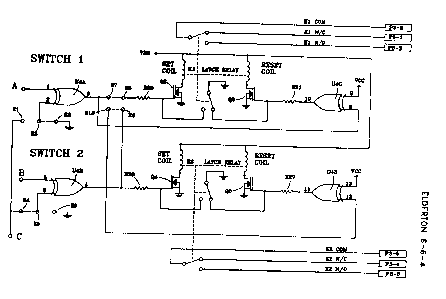
Referring now to the switch circuits, the switching of the
~ `~
1~24~3~ ~
voitage comparator depend~ on the po~ition o~ the positlon pot
R10 Or FIG. 1B relative to the set point pot which may b~ either
RS or R6 in FIG. 1B. since this is a null measurement, a stable
volta~e across the pot~ntiometer circuit i9 not required When
the position POt R10 iS ~PSCa1e from the set point, ~or example
R6 the comparator U3~ output will bQ 10W. If E2 in FIG. 1A iS
~umpered to E3 aS shown u4A will function ae a non-inverting
buffer with its output also 10W. If E7 iS jumpered to E8 aS
shown in FIG 1~ the gate of Q2 will be bia~ed low pr~venting Q2
fro~ conducting Since the input to U4C at a i~ low its output
will b~ high~ This would bias Q3 in the conducting state except
that the gate is grounded by contact~ of Kl
When the position pot R10 i9 down ~caled from the set point
R6 the comparator U3~ output will be high and the output of U4A
will be high~ T~e g~t~ o~ Q2 will charge to th- high pot~ntial
through R20 causing it to conduct curr~nt through th~ ~-t coil
of Xl latch relay Kl will switch the contacts reversing the
position shown and short the gate of Q2 to ground This will
cause Q2 to be nonconducting and current will cease flowing
through th- set coil ThQ rel~y is magnetically latched in this
state~
Th~ resistor n~twork compo~Qd of RlC through R19 in FIG lB
provide_ hysteresis for the voltage co~parator U3A input The
hystere~is is nor~ally about 3% of FS The hysterQsis can be
increaQ~d by increasing the value of Rl9
The low batt~ry det~ctor circuit of FIG lD USQS U8 which
h~- ~ 1 15 volt r~renc~ When the input at pin 3 of U8 is
blgber th~n 1 15 volti~ the output at pin 2 is high R28 and R29
- divid~ the battery voltag- from the batterie~ BTl and BT2 for
the input at pin 3 RNSD and R30 add a small amount of h~stere-
~is in series wit~ th- volt~ge divider With pin 2 of U8 high,
Q10 will conduct, effectively qrounding the positive input of
pin 5 of voltage comp~r~tor U9B. The output Or U9B oh pin 7
w~ll r~main at logic low Under low battery conditions, for
exampl~ 1Q~;~ than 4 7 volt~, the output on pin 2 of U8 will be
low which will biaQ Q10 o~f and eEfectively disconnect ground
" ~324~3
f~rom t~e ~oltage comparator positive input. U9B is connected as
~ a~table multivibrator which produces an output that alter-
na~oly is low for 90 seconds and high for 2 seconds. The low
period is c~ntrolled by C14 and R32 ~ R33. The high period is
. 5 determined by C14 and R32 since the diode CR8 shunts R33.
Th~ outp~t of the low battery circuit is used to momentari-
ly reverse the position of one or both switches by connecting
the circ~it to the exclusive-OR circuit~ U4A and U4B with
jumpers El to E2 and E4 to E5.
. The relay coils require 40 milliamps to change state. This
far exceeds the capability of the 2 milli~mp referenc~ current
available ~rom U2. A large capacitor could store sufficient
charqe to supply this current but repeated switching at a rapid
rate would deplete this charge ~aster than it could be rQplen-
ished and the rQlay could hang up in an in between statQ where
there is no contact to either N/C or N/0. To circumvent this
problem, the relay coils are energized from th~ battery.
A second set point on R5 may be compared with the position
potentio~eter R10 in the comparator U3B as described above thus
providing, for example both a high and a low alarm or actuator
circuit. Connecting jumper Ell to E12 instead of E13 slaves
switch 2 to switch 1 enabling a second set of relay contactC
with a single set point. Jumpering E7 to E8 and E10 to E9, as
shown in the sche~atic, permits operation of the two switches
with separate set points. Note that the set points can be in
any order. For example, set point 1 can be above or below set
point 2 and they can be anywhere between zero and full scale.
Jumpering E7 to E10 and E8 to E9 causes set point 1 to
control the reset coil of Kl whereas set point 2 controls the
set coil. Similarly, SRt point 2 controls the reset coil of X2
and set point 1 controls the set coil. This combination
provides controller function with an ad~ustable hysteresis.
Typical values ~or the components shown in the circuit
diagra~ are as follows: ~
Ul is an LM 285 - 2.5
U2 is an XTR 101
1 3 2 4 ~ 3 1
U3A and B is a TLC3702
U~A and B, C and D, is a 4070
U8 is an ICL8212
! UgB is a ~LC3702
CRl and C~2 are lN914 A's
CR3 is a VM18
CR4 and CR5 are ICTE36's
CR7 and C~8 are lN914 A ' s
Ql is a 2N2222
, Q2, Q3, Q4, Q5 and Qlo ar~ VN lOX'~
Cl - l,000~V 10 V
C2, C3, C4 and C5 ar~ .Ol~f
C6 - .Ol~f/200 V
C13 - .l~f
C14 - 4~f
Rl - 6~65Kn
R2 - 8.87Kn
R3 - 22.1Kn
R~ - 4.99xn
R5 ~nd R6 - looxn pots
R9 ~ sxn pot
R10 ~ 20xn pot
Rll - 22~lxn
R12 - l9.lxn
R13 - 4.32Kn
R14 - 2~4R
.
R15 - 500 o~ pot
R16 - looxn
~"~ R17, ~nd R18-22Mn
:30 Rl9, R20 and R21 - 2.2MR
R22 - looxn
-- R23 ~nd R24-22Mn
-~ ~ R25 - 2.2Nn
R26 ~nd R2~-2.2NR
: 35 R28 - lONn
R29 - 3Nn
8 ``
:
.
~"
132~31
R30 - 20K~
R31 - 22Mn
R32 - 220Kn
~33 - 22M~
RN5A - RN5D are 4 2 2mn network resistors
Ll - 5 millihenries
BT-l and BT-2 - BR - 2/3A 3V lithium
Again the circuit is used to rQplacQ pre8ent mechanically
actuated switches coupled to a meter movemQnt such as shown in
10 ~ FIG. lB which ~ay be, for example, a Barton pressure and delta
pr~ssur~ gage When a pre~sur- is appliod to high and low
chambers surrounding b-llow~, any differenc~ in pressure causes
the b~llows to ~ov~ until the spring effect of the unit balance~
out force thus gen-rated The lin-ar motion of tho b-llows
which is proportional to the differential pres-ure is trans-
mitted as a rotary ~otion through the torque tube asse~bly For
a direct functional replacement in ~uch a unit external power
may not be available and the circuit is battery opQrated and
features long batt~ry life Novelty rQsides in the mQthod of
op rating DPDT ~agnetic latching relay~ so as to minimizQ
battery current drain onQ set of the relay contacts in ~IG lA
are us-d to turn off th~ MOS transistor~ Q2 through Q5 that
enargiz- the relay~ windings after the relay switch is posi-
tioned In the circuit shown the wiper o~ R10 is mechanically
coupl~d to th- dial mechanism or meter movement The adjustment
of R5 or RC represents a ~witch ~etting desired The output o~
U3A pin 1 will bo at ground potential i~ th- voltage potential ~ ;
or th~ ~lpor or R10 1-~ mor~ than a ~ew mllllvolts mor~ posltive
th~n the wiper of R6, R16, 17, 18 and 19 providing a small
hyst-re~i~ E7 and E8 are shortod as are E9 and E10 for
purpo~es of this di~cus~ion If U3A pin 1 ~s at ground then U4A
pin 3 will be high and U4C pin 10 will be at ground ~ith the
relay contacts posltioned a~ shown, tho gate o~ Q2 will charge
positiv~ly causing Q2 to conduct energizing the set coil of K1
This action will causQ the relay of the switch from the state
shown to the closing of th~ contacts, grounding th~ gate of Q2
g
. . .
- 132~31 t
The gat~ o`f Q3 will remain at ground sinc~ the output of U4C is
ground. wit~ th~ gate of Q2 grounded by t~e relay contacts
current will flow through R20. To minimize this drain on the
battery R20 is made as larg~ as practical. U3A, U3B, U4A and
S U4B are CMOs circuits and consume very little current. The
potentiometers are the ma;or current drain on the battery. One
ampRre hour of battery lifo is sufficient to switch the r~lays
many ~illions of timeQ.
While a particular embodiment of the invention ~as been
, described, it will be understood of course that it is not
intended to limit t~e invention thereto ~ince many modifications
may be made. It is t~erefore contemplated by the appended
claims to cover any such modifications as fall within the true
-spirit and scope of t~e invention.
"`
~_ _ ,,.j .