Note : Les descriptions sont présentées dans la langue officielle dans laquelle elles ont été soumises.
~3278~3
HEATER FOR IONOG~APHIC ~IARKING HEAD ARRAY
Field of the Invention
5 This invention relates to an ionographic marking head array having a
heater in proximity thereto for elevating the temperature of the modulation
electrode region of the array so as to prevent the accumulation of moisture
upon the substrate in the electrode region.
10Background of the Inv~ntion
Ionographic marking systems are disclosed in commonly assigned U.S.
Patent Nos. 4,584,~22 and 4,719,481. In each, a fluid jet assisted ion
projection marking device places imaging charges upon a moving receptor
15 surface, such as paper, by means of a linear array of closely spaced minute
air "nozzles". The charge, comprising ions of a single polarity (preferably
~; positive), is generated in an ionization chamber, upstream of the "nozzles",
by a high voltage corona discharge and is then transported to and through
the "nozzles", where it is electrically controlled by electrical potentials
20 applied to an array of marking elements, in the form of modulation
electrodes, one associated with each "nozzle". Selecti~ control of the
electrical potenbal applied to each of the modulation electrode in the array
will enable areas of charge and areas of absence of charge to be deposited on
the receptor surface for subsequently being made visible by suitable
25development apparatus. ~ ~
~ . ~ . . .. .
; - , . . .
, , ~ . ,;
-~
~32783~
A marking head of page width, i.e., about 8.5 inches wide, having a
resolution of 200 to 4~0 spots per inch (spi) would result in an array of 1700
to 3400 modulation electrodes. Typically, for a 300 spi writing head, each of
5 the modulating electrodes would be about 2.3 mils wide and have an
interelectrode spacing of about 1 mil. The head array is divided into a
number of sections of the modulation electrodes, arranged so that each
section may be sequentially isolated and addressed by a compact,
multiplexed, data loading circuit, integrated upon the head array substrate
10 for bringing each of the modulation electrodes to the desired voltage (û volts
for "writing" or 10 to 30 volts for "non-writing"). Gray scale also may be
achieved by imposing intermediate modulation voltage values on the
modulating electrodes, for placing intermediate charge values upon the
receptor surface which, when developed, e~hibit a range of optical densities.
1~
In 4,584,522 the modulation electrodes in each selected section are rapidly
brought to the predetermined control voltage when coupled to data buses
during a short segment of the entire line writing time. After being loaded
each section is decoupled from the data buses and each modulation electrode
20 will hold its applied voltage ("float") for the remainder of the line writingtime. Typically, loading of each section can be accomplished in about 2.6%
of the line writing time, allowing the modulation electrode to float for about
97.5% of the line writing time, until it is again addressed.
.
~ ' :, '~: ' . ' ', '. . .,, ' , . : :
~327~3Z~
The data loading circuit in 4,71~,481 allows the modulation electrodes in
each selected section to be directly connected to either a source of writing
potential or a source of non-writing potential, each being supplied by a
5 suitable bus line. In practice, the electrodes are held at either a reference
(i.e. ground~ potential, or a higher (1~ to 30 volts) potential, respectively.
While there are certain aclvantages to be derived from always maintaining
the correct potential on the modulation electrodes, a disadvantage is that
marking latitude is limited because it is not possible to apply a potential of
10 any desired intermediate value as is necessary for gray scale marking.
In high humidity conditions, e.g., RH~50%, we have observed the
occurrence of image blurring, or smearing, during operation of the marking
device incorporating the head array of the 4,584,522 type. This has been
15 attributed to interpixel current leakage. It was further observed during
test;ng, that image blurring did not occur until after the marking head
array had been exposed to corona effluents.
It is the primary object of this invention to provide an improved marking
20 head array in which marking will be virtually unaffected by high humidity
conditions.
It is another object of this invention to provide an improved marking head
array which is heated for eliminatingmoisture collection upon its surface.
~5
~ , ~
::: `. :
: ,
- 1327~3
Summary of the Invention
The present invention may be carried out, in one form, by providing an
5 ionographic marking apparatus including a housing, means for generating
a supply of marking ions within the housing, means for transporting the
marking ions through and out of the housing, and means for controlling the
transport of the ions out of the housing. The means for controlling
comprises a substrate provided on one surface with an array of electrically
10 conducting ion modulation electrodes spaced from one another by
electrically insulating regions, and the improvement comprises heating
means associated with the means for controlling for raising the
temperature of the electrically insulating regions so as to prevent the
condensation of moisture thereon.
: ~ Brief Description of the Drawings
Other objects and further features and advantages of this invention will be
apparent from the following, more particular, description considered
20 together with the accompanying drawings, wherein:
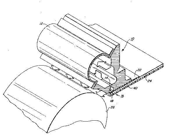
:~ Figure 1 is a perspective view showing an ionographic marking head,
Figure 2 is a side sectional elevation vlew showing a portion of the marking
25 head of Fig. 1,
1327833
Figure 3 is a schematic representation of a marking array including the
control circuitry,
Figure 4 is a schematic representation of a moclulation structure showing
"writing",
Figure 5 is a schematic representation of a modulation s$ructure showing
"writing" being inhibited, and
Figure 6 is a plot of ion current and optical density as a function of
modulation electrode voltags.
Detailed Description of the Illustrated Embodiments
: With particular reference to the drawings, there is shown in Fig. 1 an
ionographic marking head 10. The upper portion of the head defines a
plenum chamber 12 to which is secured a source of transport fluid (not
shown~, such as air supplied by a blower. An entrance channel 14 delivers
20 the air from the plenum chamber to an ion generation chamber 16, of
ge~erally U-shaped cross-section, having three side walls surroundin~ a
corona wire 18. All three of the walls of the ion generation chamber may be
electri~ally conductive, although it is possible to make only the side wall 20
(the one closest to the wlre) conductive and the remainder of the walls
26 insulating. Thus, one has great latitude in ~abricating the marking head
~ .
: . .
.
,
1327~3~
10; it may be made of a conductive material such as metal or a conductive
plastic, or it may be made of an insulating material with certain significant
portions coated with a conductive material. Suitable wire mounting
supports (not shown) are provided at opposite sides of the marking head
5 body for adjusting the mounting of the wire 18 to the desired location within
the chamber 18. A plate 22, preferably made of conductive material, is
urged against the marking head body to complete the chamber 16 by closing
a major portion of the open end of the U-shaped cavity. As best seen in
Fig.2, the plate is spaced from side wall 20 to allow ions to exit the chamber.
A planar substrate 24, made of an insulating material, such as glass,
supports the thin film electronic control elements and modulating
electrodes of the marking array. The thin film elements are represented by
the marking array layer 26 and are more specifically described with a
15 reference to Fig. 3. An insulating layer 28 is sandwiched between the
substrate 24 and conductive plate 22 to overcoat and protect the thin fîlm
electronic control elements and to electrically isolate them from the plate
22. A spring clip or other suitable biasing means ~not shown) urges the
substrate 24 and the plate 22 together and into place with sufficient force to
20 flatten irregularities in each oE these planar members, so as to define an
accurately and uniformly configured dog leg exit channel 30 between the
end of plate 22, the upper end surface of the substrate and the electrically
conductive end wall 32 of the markillg head which is connected to a source
of reference potential, such a ground. The generally L-shaped exit channel
25 30 includes an ion generation chamber exit region 34 and an ion modulation
. ~ .................... .,, .... ~ . . .
- ~ , ~ , . . . : . . . .
1327833
region 36. Thus, transport air ~lows through the head as represented by the
arrows in Fig. 1: through the plenum chamber 12, into the ion generation
cavity 16 via the entrance channel 14, out the exit channel 30, to impinge
upon the receptor surface 38. A thin heater element 40 (to be described
5 below) is secured to the bottom surface of the substrate 24.
The marking array 26, of the present invention, illustrated in Fig. 3, may
include, in its simplest form, an array of moclulation electrodes (E) 42,
positioned along one edge of the substrate 24, and a multiplexed data entry
10 or loading circuit, comprising a relatively small number of input address
bus lines ~A) 44 and data bus lines ~D) 46, and thin film switches 48. As
shcwn, each modulation electrode 42 is connected to the drain electrode 50
of a thin film transistor 48, an address bus line 44 is connected to its gate
electrode 52, and a data bus line 46 is connected to its source electrode 54.
15 The multiplexing arrangement comprises p sections or groups, each section
having q electrode/switch pairs. In our present embodiment the 2560 pixel
elements are divided into 40 sections (p=40) and 64 electrode/switch pairs
(q = 64). Each of the p address bus lines is addressed sequentially so as to
address a selected section and each of the q data bus lines simultaneously
2a brings the modulation electrodes of the selected section to the
predetermined volta~es. When an activatlng signal from the external IC
address bus driver 56 is applied to the Amth address bus line, every one of
the q thin film switches in the mth section is turned ON while the thin film
switches of all other sections remaiIl OFF. The q modulation electrodes 42
25 in the mth section will be charged or discharged to electrical potentials
. . . .
; ~ :
.
.
1~278~
substantially equal to those supplied to the q data lines by the external IC
data bus drivers 58. Then the thin f~llm switches in the mth section will be
turned OFF simultaneously anà the thin film switches in the (m+l)th
section will be turned on by pulsing the address bus line A(m+ l). At the
5 same time, new data will be supplied to and appear on the q data bus lines
so that the modulation electrodes in the (m ~1)th section will be charged or
discharged to potentials corresponding to the new data on the data bus
lines.
10 As described, loading of information is time multiplexed, i.e. the
modulation electrodes in each section are loaded in about 2.5% of the line
time, and then they act to control the ions passing through the exit channel
30 during the remaining about 97.5% of the line time. Since the thin film
switches of each section are switched OFF after the modulation electrodes of
15 a selected section have been charged to the predetermined data input
voltages, each modulation electrode "floats" at, or near, its applied voltage
until its associated switch is again turned ON for loading the next
increment of line information.
20 In Figs. 4 and 5 there is illustrated the "writing" and "non-writing"
conditions, respectively. Ions entrained in the transport fluid passing
through the modulation region 36 come under the influence of fields
established between the modulation electrodes 42 and the end wall 32.
"Writing" of a selected spot (Fig. 4) is accomplished by connecting a
25 modulation electrode 42 to the reference potential source 60, via switch 48,
,, , . .. ; : ,~
"
.
13~7833
so that the ions, passing between the grounded modulation electrode and
the grounded end wall, will not see a field therebetween and will pass to the
receptor surface 38 where it will be made visible, subsequently.
Conversely, when a modulation electric fïeld is present between these
5 elements, as by closing switch 48 and applying to the modulation electrode
the desired potential from source 62, the established f1elds will repel ions to
the grounded end wall. The ions driven into contact with the end wall 32
will recombine into uncharged, or neutral air molecules so that the
transport fluid exiting from the modulation region 36 will carry no ions to
10 the receptor surface. Since the potential source 62 may be selected to be anydesired value, it is possible to deflect less than all of the ions passing
through the ion modulation region, allowing only some ions to deposit on
the receptor surface, thus "writing" many desired levels of gray.
~; 15 If the modulation electrodes are not held at the required voltages during
binary "writing", the otherwise desirable feature of gray scale '~writing"
may become objectionable. This can be seen more clearly with reference to
the characteristic curve illustrated in Fig. 6. The curve represents ion
current (nA/cm) and optical density of a visible mark on the receptor
20 surface, as a function of modulation voltage (the values for ion current are
indicated on the Y-axis). Optical density ~degree of black) of the image is
effected by the development and transfer systems and is proportional to the
ion current represented by the number of ions which have passed out of the
marking head and have been deposited upon the receptor surface. For
25 binary "writing" it is desirable to operate at the end portions of the curve
,.. " ., .. , . , ., ~ - , . ~
, . .. . . . . .
- - . :; .... ... : i -~; ; ,
.,, ~. -
,.,,
,., . ., , .. " ~ ~ , .
. . . , , , ~- .
.. . ..
~3~7~3~
(i.e. in the vicinity of 0 volts for "writing" and at about 8 volts, or greater,for "non-writing"). Black pixels will occur at modulation voltages at, or
near, 0 to 2 volts, while white pixels wili occur at modulation voltages at, or
above, a threshold voltage of about 7 volts. Intermediate to these values, in
5 the regions where the slope of the curve is the greatest, different levels of
gray will be printed.
It has been observed that during operation of the ionographic marking
device in high humidity conditions, e.g., R.H. > 60% there is distortion of the
10 desired ion output between electrodes "floating" at different modulation
voltages. This phenomenon is attributed to interelectrode current leakage
caused by a combination of the atmospheric conditions and the corona
ef~uents. In the binary mode of operation, the result may be a fuzziness,
rather than a crispness, at the edges of characters. In the gray scale mode of
15 operation, humidity e~fects are even more disconcerting since it is critical,in order to achieve the proper optical density, that accurate volt~ge levels
be applied. Any departure from the desired modulation voltage value will
cause gray levels to be skewed.
20 During operation of a typical ionographic marking device, data voltages, on
the order of 0 volts and 16 volts, are applied. On the higher voltage
electrodes, it can be expected that the modulation electrodes will only
achieve about 13 volts during the very short addressing time. However, if a
conductive path exists between two adjacent electrodes charged to di~erent
25 potentials, the 13 volt electrode will lose a good deal of its charge to its
--10--
.. ", ~, . . .
:, . , , : ~, . . .
1327~3`~
neighbor over the remainder of the line tirne. For example, if about half the
charge leaks off the higher voltage electrode and collects on the lower
voltage electrode, both electrodes will reach equilibrium at about 6 volts.
Then, as can be seen from Eiig. 6, both electrodes will "write" gray, rather
5 than the 0 volt electrode "writing" black and the 15 volt electrode "writing"
white. As a result, the desired mark will be broadened and fuzzy. This
same problem exists at the interface of black and white areas, wherein the
crisp boundary hecomes gray and fuzzy.
10 If, on the other hand, the data voltage is on the order of 20 or 30 volts, and
the same interelectrode current leakage conditions exist to an adjacent 0
volt electrode, it can be e2cpected that both electrodes will reach equilibrium
at about 10 to 15 volts. As can be seen from Fig. 6, both electrodes will
"write" white, rather than the 0 volt electrode "writing" black and the
15 higher voltage electrode "writing" white. In each case, the desired contrast
between the output of the electrodes is lost, and image smearing takes
place.
These printing aberrations are attributed to inter-pixel current leakage due
20 to the establishment of a conductive path of water overlying the glassy
interelectrode subskate surface. Normally, the head array contains
hydrocarbon contamination upon its sur~ace which makes adsorbed water
bead on the interelectrode surfaces. Therefore, no continuous conductive
paths are provided between the modulation electrodes. As presently
25 u~derstood, it is believed that the corona effluents provide a scrubbing
--11--
, ;, ,.. ,, ~ . ~,
, ~ . . . ,,, . ,
, . . .
, ! ` . ~ ~ ,
~' ' '
~27~33
action which cleans accumulated hydrocarbons off the array surface. It has
been found that in addition to the ions created by the corona discharge,
within the ion generation chamber 16, there is also ozone, and numerous
oxides of nitrogen (N20, N02, NO), as well as the excited states of these
5 gases, which are far more oxidizing than their non-activated states. In
higher humidity conditions, where water is available, acids of nitrogen are
also present. After the array surface has been cleaned by the highly
reactive corona effluents, the wetting property of the interelectrode
substrate surface is improved and the contact angle of the water condensed
10 thereon approaches 0. A thin and continuous layer of water will then
provide conductive paths between the "floating" electrodes.
It has been found that one way to eliminate these conductive paths is to
heat the marking array surface su~ficiently to prevent condensation, or
1~ adsorption, thereon. Heating the array in the range of 100F to 130F
provides a sufficient increase in temperature to compensate for the absolute
moisture in an 80% to 85% relative humidity environment.
As shown in Fig. 2 the thin heater element 40 is secured to the underside of
20 the planar substrate 24, as by adhesion, so as to obtain a good thermal
coupling. The heater comprises a sandwich of polyimide ~e.~. Kapton~)
layers 64 enclosi;lg resistive metal traces 66 which are connected to a
suitable power supply. As implemented, a steady state power supply (of
about 2.6 watts) has been found to be adequate to maintain the substrate at
25 the proper temperature. In this configuration, the heater is always ON as
--12--
1327833
long as the machine is plugged in, so that the machine is always ready to
"write" and there is no need for energizing a moisture driving heater when
the signal is given to "write", which would introduce a delay into the
writing cycle. The constant wattage, always ON, combination minimizes
5 cost by eliminating the need for any temperature control circuitry.
The conductive heater element may comprise a metal such as nichrome, in
wire form or as a foil. Also suitable as heater element materials are tin
oxide, indium oxide or mlxtures thereof, or other metal oxides or conductive
10 ceramics. Although the heater 40 is shown to be adhesively secured to the
substrate, it is also possible to evaporate or paint th;n films of heating
material directly onto the substrate. Preferably, the heater material should
have a high resistivity in thin film form, so that a reasonable voltage of
about 12 to 15 volts, can be applied across it without generating a great deal
1~ of power. More recently a low watt density, self controlling, heater material has been developed whose conductivity decreases as it heats up, thus
limiting itself to a desired, predetermined, temperature. Other heater
choices, such as radiant or convective, may also be suitable.
20 It should be understood that the present disclosure has been made only by
way of example, and that numerous changes in details of construction and
the combination and arrangement of elements, may be resorted to, without
departing from the true spirit and scope of the invention as hereinafter
claimed.
--13--
~1 .