Note : Les descriptions sont présentées dans la langue officielle dans laquelle elles ont été soumises.
- 132983~ -:
SPECIFICATION
Title of ~e In~lention - `
CODE VIOLATION DETECrION CIRCUIT FOR ~ -
USE IN AMI SIGNAL TRANSMISSION
Background of the Invention ~ -
Field of ~e invention
The present invention relates to a code violation detecting circuit, -and more specifically to a circuit for detecting a code violation in the
transmission of a signal transmission system in accordance wi~ the
CCIl~-I430, regardless of a connection polarity of the transmission line.
Desc~iption of related art
Recently, the demand for digital data communication is increasing
year after year. Under this circusnstance, the CCITT (International
Telegraph and T¢lephone Consultative Committee) advances an
international standard for ISDN (Integrated Services Digital Network). ; ~
One typical standard i8 a so called "altemate mark inversion" (AMI) ~ ;
signal.
In ~is AMI signal, a first binary logic level of for example "0" i8 ~ ;
alternately expressed by a first po}arity 8ignal and a second polarity signal
djfferent from each other in polarity, and a second binary logic lével "1"
complemen~ary to the first binary logic level "0" is expressed by a signal
diffe~ent in potential level from each of the flrst and second polarity
signals. The code violation is realized by continuous occurrence of two
,~ ', , ,1 $' ''''''~'''''''"'~
, . .,; . .
132~36 ;
same polarity signals within a predetermined period starting from a start
o~ each ~rame without interlea~ ing the o~er polarity signal.
In the pri~r art, a detection of the code violation has ~een
perforrned by detecting the continuous occurrence of two same polarity
signals within the predetermined period without interleaving the other
polarity signal, since ~e S point is not necessarily connected in a proper
condition. However, the continuous occurrence of two same polarity
signals without interleaving the other polarity signal will appear, not only
at the code violation portion in each signal frame, but also at a boundary -
between each pair of continuous frames, for example given by a framing
bit and a data bit which is included in the just preceding frame and which
has the the same polarity as that of the framing bit. As a result, only dle
correct code violation carmot be detected in the prior art violation
detection circuit.
Sun~nary of the Invention
Accordingly, it is an object of the present invention to provide a
code violation circuit which has overcome the above mentioned defect of
~e conventional one.
Another object of the present invention is to provide a code
violation circuit for the AMI signal which can detect only a correct code
violation in each frame.
The above and other objects of the present invention are achieved in
accordance with the present invention by a circuit for detecting a code
violation in an alternate mark inversion signal in which a first binary
lo~ic level is alternately expressed by a first polarity signal and a second
polarity signal difforent from each other in polarity, and a second binary
,
.. :.,. , ,.,:':. . '
., .
132983~
logic level complementary to the first binary logic level is expressed by a
signal different in potential level from each of the first and second
polarity signals, the code viola$ion being realized by continuous
occurrence of two same polari~y signals without interleaving the other
polarity signal, comprising a first detecting circuit receiving the alternate
mark in~ersion signal for generating a first detection signal at continuous
occurrence of two first polarity signals without interleaving the second
polarity signal; a second detecting circuit receiving the alternate ma*
inversion signal for generating a second detection signal at continuous
occurrence of two second polarity signals wi~out interleaving the first
polarity signal; a first enable signal generating circuit receiving the first
detection signal for ~enerating a first enable signal having a
predetermined active period; a second enable signal generating circuit
~eceiving the second detection signal for generating a second enable signal
having a predetermined active period; a first violation detection circuit
receiving the second detection signal and the first enable signal for
generating a first code violation detection signal when the second
detection signal i8 generated during the active period of the first enable
siBnal; and a second violation detection circuit receiving the first detection
signal and the second enable signal for generating a second code violation
detection signal when the first detection signal is generated during the
active period of the second enable signal.
With the above mentioned arrangement, the connection polarity of
the transmission line is automatically detected on the basis of the input
data, and thereafter, the code violation is detected with reference to the
detected connection polarity.
",,,, ~,
', ;'.; ,
r~ .s . ' . '.
132i~8~
The abo,ve and other objects, features and advantages of the present -
invention will be apparent from the following description of pre~erred :
embodiments of the invention with reference to the accompanying ::drawings.
Brief Description of ~e Drawings ~ ~
Pigure 1 is a block diagram illustrating a CCI~ standard model of ~ -
an interface for the ISDN;
Pigure 2 is a diagram illustrating a frame structure and a channel
structure on the S point shown in Figure l;
Figure 3 is a waveform diagram illustrating the code violation in
the ISDN format;
~ igure 4 is a block diagram of a conventional code violation
detecting circuit;
~ igure 5 is a waveform diagram illustrating an operation for
detecting the code violation in the case that the S point is correctly ;:connected;
~igure 6 is a waveform diagram illustrating an operation for ~ .detecting the code violation in the case that the S point is inversely
connected;
Pigure 7 is a block diagram of an embodiment of the code violation
detecting circuit in accordance with the present invention; and .~ igure g is a timing chart illustrating an operation for detecting the
code violation in tho circuit shown in Figure 7. ~
': .
132~83~ ~
Description of the Prefe~ed embodiment
Referring to Figure 1, there is shown a block diagram illustrating a
CCll~ standard model of an interface for the ISDN.
In Figure 1, a terrninal equipment TE is a boundary between a line
system and an ~fflce channel system, and is connected to a network
tenninator NT. A transmission line between the terrninal equipment TE
and the network terminator NT is called a S point, which is constituted of
a bus composed of four lines according to the ISDN, so that two lines can
be assigned for each of transmission and reception.
Turning to Figure 2, there is shown a diagram illustrating a frame
structure and a channel structure of data transferred on ~e S point shown
in Figure 1. The fonnat of the shown signal is lOO~o-AMI signal, and a
binary value "1" is represented by "no-signal", and a binary value "O" is
indicated by a positive or negative pulse. For the following explanation,
the binary value "O" indicated by the positive pulse is denoted by "+O" and
the binary value "O" indicated by the negative pulse is denoted by "-O" ;
In a basic AMI signal, "+O" and "-O" alternately appear. But, in the
ISDN format, a code violation is introduced for a frame synchronism.
~igure 3 illustrates the code violation in the ISDN format.
In I7igure 3, a first bit of each frame is a framing bit F, which is
followed by a balancing bit L constituted of "-O". A binary value "O"
firstly appearing after the balancing bit L is forcedly made to "-O", so that `
t vo binary values "O" havin~ the same polarity will successively appear.
Thi8 continuous occurrence of the two binary values having the same
polarity constitutes the code violation. In the ISDN format, ordinarily,
the code violation is set to appear within 14 bits from the framing bit F, ~ ~
'' ' :'
:. ...
S , ., ~
,' " ~''' "
,i . . ... ..
132~83S :
so th~t the detection of the code violation will give the frame -
synchronism. -
In the meantime, if the S point is correctly connected, the code
violation can be detected as ~e continuous occurrence of the two "-0"s.
However, the CCIl~ recommendation requires that even if the S point is
inversely connected, the code violation can be properly detected.
Therefore, it is necessary to detect the continuous occurrence of the two
"+O"s.
Referring to Figure 4, t}lere is shown a block diagram of a
conventional code violation detecting circuit.
The shown circuit includes an AMl/binary conversi~n cireuit 10
having a pair of inputs INl and IN2 connected to a pair of input terminals
12 and 14, which are connected to a pair of lines of a receiving bus of the ~
S point. The conversion circuit 10 generates a first binary signal ;
corresponding to "~0", and a second binary signal corresponding to "-0".
The~e binary sjgnals are inputted to a "+O" code violation detection circuit
16 and a "-0" code ~violation detection circuit 18. The "+0" code violation
detection circuit 16 detects the continuous occurrence of two "+0"s, and
generates a detection signal to an output terminal 20. On the other hand,
the " 0" code violation detection circuit 18 detects the continuous
occurrence of two " 0"s, and generates a detection signal to an output
terminal 22.
17igure 5 illustrates an operation for detecting the code violation in
the case that the S point is correctly connected, and Figure 6 illustrates an
operation for detecting the code violation in the case that the S point is
inversely connected. Now, ~e operation of the circujt shown in Figure 4
will be explained with reference to 17igures 5 and 6,
2'~ : .
'", "; `. - ~ ?
~32~83~
Namely, as seen from Figur~s S and 6, ~e AMI/bina~y conversion
circuit 10 outputs a signal of "1" (a positive pulse) to a node "a" when
"+0" of the AMI signal is detected, and a signal of "1" to a node "b" when
"-0" of the AMI signal is detected. On ~he other hand, when "1" of the
AMI signal is detected, the AMIlbinary conversion circuit 10 outputs a
signal of "0" (a base level) to both of the nodes "a" and "b". -
'rhe "~0" code violation detection circuit 16 outputs a detection
signal of "1" to an output terminal 20 when it detects the continuous
occurrence of two "1"s on the node "a" within a period of 14 bits without
interleaving the "1" on the node "b", as shown in Figure 6. On the o~er
hand, the "-0" code violation detection circuit 18 outputs a detection signal
of "1" to an output terminal 22 when it detects the continuous occurrence
of two "1"s on the node "b" within a period of 14 bits without ~ .
interleaving the "1" on the node "a", as shown in Figure S. ;
As a result, if the S point is correctly connected, the code violation
i8 detected by the "-0" code violation detection circuit 18, as seen from .
~igure 5. However, if the S point is inversely connected, the code :
. ....
violation i8 detected by the "~0" code violation detection circuit 18, as :
seen from ~igure 6.
Actually, the continuous occurrence of the two "0"s having the same
polarity in the AMI signal will appear in a period other than the code
violation period as shown by Reference Character "A" in Figure 3. For ; : .
example, in the case shown in Figure 3, a framing bit F and a last "0" data ::bit in the just preceding frame have the same polarity (See a period "B"). :
.... ....
The framing bit P and the last "0" data bit in the just preceding frame are :
oppo~ite in polarity to that of the code violation in the period "A".
However, it will be detected by the "~0" code violation detection circuit .
, : .:;.
132983~
18, if tbese bits appear within a peri~d of 14 bit~. In an actual data
transmission, this would have a sufficient possibility.
Acc~rdingly, the circuit sh~wn in Figure 4 capable of detecting the
continuous occurrence of "0" having the same polarity within ~e 14-bit
period, is not sufficient in properly detecting only the code violation for
the frame synchronism.
In this connection, it may be considered to determine the connection
polarjty of the S point on the basis of probability by comparing the
numbers of appearance of the detection signals on the detection outputs 20
and 22. ~his would require a ve~y large size of circuit, and in addition,
cannot perfectly assure the correct detection.
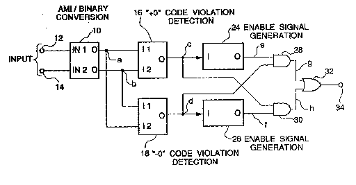
Referring to ~igure 7, there is shown a block diagram of an
embodiment of the code violation detecting circuit in accordance with the
present invention. In Figure 7, circuit elements similar to those shown in
~igure 4 are given the same Reference Numerals.
The shown circuit includes an AMI/binary conversion circuit lO
having a pair of inputs IN1 and IN2 connected to a pair of input terrninals
12 and 14, to which are connected a pair of lines of a receiving bus of the
S point, The conversion circuit 10 genera~es a first binary signal
corre~ponding to "+0" onto a node "a", and a second binary signal
corresponding to " 0" onto a node "b". These bjnary signals are inputted
to a pair of jnputs I1 and I2 of a "+0" code violation detection circuit 16
and a pair of inputs I1 and I2 of a "-0" code violation detection circuit 18.
The "+0" code violation detection circuit 16 detects the continuous
occurrence of two "l"s on the node "a" wi~in a period of 14 bits without
interleaving tho "1" on the node "b", and generates a first detection signal
of "1" when the continuous occurrence of two "l"s on the node "a" is
,' ': ,
.,
.'
132~83~
detected. On the other hand, ~e `'-0" code violation detection circuit 18
detects dle continuous occurrence of two "l"s on ~e node "b" within a - -
period of 14 bits without interleaving ~e "1" on the node "a", and
generates a second detection signal of "1" when ~e continuous occurrence
of two "-0"s on the node "b" is detected. -
The first detection signal is inputted from the "+0" code violation -
detection circuit 16 through a node "c" to a first enable signal generating
circuit 24, which generates a first enable signal having an active period
corresponding to a 14-bit period. The second detection signal is inpu~ted
from the "-0" code violation detection circuit 18 through a node "d" to a
second enable signal generating circuit 26, which generates a second
enable signal having an active period corresponding to a 14-bit period.
The first enable signal is supplied from the first enable signal
generating circuit 24 through a node "e" to a first input of an AND gate
28, which in turn has a second input connected to receive the second
detection signal from the "-0" code violatjon detection c;rcu;t 18, The
AND gate 28 generates a first code violation detection signal when the
second detection signal is generated during the active period of the first
enable signal, On the other hand, the second enable signal is supplied
from the second enable signal 8eneratin8 circuit 26 through a node "f" to
a first input of another AND gate 30, which in turn has a second input
connected to receive the first detection signal from the "+0" code
violation detection circuit 16. The second AND gate 30 generates a
second code violation detection signal when the first detection signal is ~ -
generatcd during ~e active period of the second enable signal. Outputs of
~cse AND gates 28 and 30 are connected through nodes "g" and "h",
' '':'
': '
. . .
. .
..
~2~3~
respectively, to an OR gate 32, which generates a resultant code violation
deteiction signal to an output te~ninal 34.
Now, operation of the above mentioned circuit will be exp~ained
with reference to Figure 8 which illustrates an operation for detecting ~e
code violation in the circuit shown in Figure 7.
In the AMI signal exemplified in Figure 8, a framing bit F
positioned at a head of each frame and a balancing bit L located at a tail
end of each frame are formed of "+0". Therefore, at a timing tao, the
continuous occurreince of the two "+0"s is detected and the first detection
signal (indicative of the continuous occurrence of two "+0"s) is outputted
to the node "c". In response to this first detection signal, the first enable
signal generating circuit 24 outputs the first enable signal of "1" having
the 14-bit widtb to the node "e".
On the other hand, the correct code violation is fo~med of the
balancing bit L appearing just after the framing bit F, and an auxiliary
framing b;t ~A which appears at a timing tal3 after the framing bit F.
These bits are detected by the "-0" code violation detecting circuit 18, and
the second detection signal (indicative of the continuous occurrence of two
"-0"s) is outputted to the node "d", In response to this second detection
signal, the second enable signal generating circuit 26 outputs the second
enable signal of "1" having the 14-bit width to the node "~
Accordingly, at the timinB tal3, the node "e" and the node "d"
become a high level ("1"), and therefore, the AND gate 28 outputs a
signal of "1". As a result, the resultant code violation detection signal is
outputted to the output terrninal 34.
However, a detection signal indicative of the continuous occurrence
of two same polarity "0"s composed of the framing bit F (of "+0" in the
1329836
shown example) and a data or control bit of the same polarity included in
~e just preceding frame and appearing before ~e framing bit F will not
overlap with the enable signal outputtèd on the node "f", since the
detection signal is generated at the timing tbo in the case that the framing
bit F constitutes a second bit of the two continuously occurring bits of the
same polarity. Therefore, the output of the AND gate 30 is maintained at
the level of "O".
The above mentioned operation is directed to the code violation
detection in the case that the S point is correctly coMected. However, if
the S point is inversely col~nected, the AND gate 30 will output the signal
of "1" when the code violation is detected, so that the resultant code
. ... .
~violation detection signal of "1" is outputted from the terminal 34. - -Accordingly, the circuit explained above and shown in Figure 7 will
be able to detect only the correct code violation, regardless whether the S
point is connected correctly or inversely.
As seen from the above, the code violation detection circuit in
accordance with the present invention, can discriminate the polarity of the
S point connection and detect only the correct code violation, without
requiring a large size of circuit. :
The invention has thus been shown and described with reference to
the specific embodiments. However, it should be noted that the present
invention ia in no way limited to the details of the illustrated structures
but changes and modifications may be made within the scope of the ;
appended claims.
, .... ...