Note : Les descriptions sont présentées dans la langue officielle dans laquelle elles ont été soumises.
1 330648
PHN 11.440 l 1O.6.1986
Method of manufacturing a semiconductor device.
The invention relates to a method of manufactu-
ring a semiconductor device, in which a semiconductor
b~y having a major surface and one or more active regions
which are located at this major surface and which~ viewed
on this major surface, are bounded by a first partern of
field insulation having a first thickness is provided with
a masking with a second pattern having one or more openings
wh`ich are located so that through each opening at least a
part of the said one or more active regions is accessible
for doping, and in which for this doping an implantation
treatment is carried out at a given implantation energy,
the masking comprising a layer p~vided with openings made
of a semi-masking material f-r the ions used in the
implantation treatment, this layer having a second
thickness, while the given implantation energy is chosen to
be so high that in the part of the said one or more active
regions acces~ible for doping the penetration depth of
the dopant ls at least practically equal to the first
I layer thickness, the layer of semi-masking materials
¦ 20 provided with openings being a comparatively thick second ~ .
~ layer of a second material which is provided on a
j comparatively thin first layer of a first material also ::
belonging to the masking, the first and sec~nd materials ;:
being different ~rom each other and a third layer of the
25 masking being constituted by a layer of a third material :~
which is located on the second layer and has one or more
further openings, each further opening corresponding to
one of the one or more openings in the second layer, the
third material differing from the second material, the
layer of semi-masking material provided with openings
being entirely removed from the semiconductor body,
Such a method is known from European Patent ~ :
Application published on 16 March 1983 under No. 74215.
.~i, ;.
1 330648
PHN 11.440 2 10.6.1986
In this case, the masking is constituted by a thin first
layer of silicon oxide, a thicker second layer of poly-
crystalline silicon and a third layer of photosensitive
material which has substantially the same thickness as the
second layer. After the implantation treatment, a metal
layer is provided, of which the part located on the masking
is removed by dissolving the photosensitive layer. Subse-
quently, the polycrystalline silicon layer of the masking
is removed. The metal pattern thus obtained forms a
complementary mask, which accurately masks those parts of
the semiconductor body which were subjected before to the
implantation treatment. By using a second implantation
treatment with a doping of the opposite type, doped
regions of opposite conductivity types are obtained in the
semiconductor body, which accurately adjoin each other
along the edge of the masking or the metal pattern. During
the first implantation treatment, boron is implanted at an
implantation energy of 120 keV. For the second implantation
treatment, phosphor is used at an implantation energy of
20 200 to 300 keV.
In the method known from the publication
"Scalable retrog~ade p-well CMOS technology",
International Electron Devices Meeting 1981, Technical
Digest, p. 346-349, an is~iplantation treatment is carried out
25 for doping the active regions for forming a so-called
"retrograde p-well". Boron ions are implanted at a dose of
2.10 3 per cm . The penetration depth of these ions, i.e.
the depth under the surface at which after the implantation
treatment the concentration of the implanted dopant
30 practically has a maximumS is in the relevant active
regions about 1/um. The field insulation consists of a
pattern of oxide, which is obtained in a usual manner by
local oxidation of the semiconductor body. The thickness of
the pattern of field oxide, i.e. the first layer thickness,
35 is about 0.8 /um. During the implantation treatment, a
masking (not shown) is present on the semiconductor body,
which masking covers a number of the active regions and has
r-~ ~
. .
; .
- PHN 11.440 3 1 3 3 0 6 4 8 10.6.1986
~penings at the area of other active regions, within which
openings besides the relevant active region also an
adjacent part of the field oxide surrounding this region
is always disposed. The implanted dopant penetrates within
the openings both in the active regions and under the part
of the field oxide not covered by the masking into the
semiconductor materi~l ofthe semiconductor body. On the
assumption that the penetration depth (the so-called
"range") in silicon dioxide is approximately equal to that
in silicon, the maximum doping concentration, which in the
active regions lies about 1/um under the semiconductor
surface, will be situated under t~e field oxide at a depth
of about 0.2/um. Consequently, after the treatments at high
temperature r~quired for the manufacture of the complete
integrated circuit, the surface concentration of the
doping of the "p-well" in the parts located under the
field oxide is comparatively high, as a result of which
a specific doping treatment for obtaining p-type channel
stopper zones adjoining the field oxide may not be
required. In this case, as a result of the said compara-
tively high surface concentration under the field oxide,
the parasitic threshold voltage for channel formation under
this oxide in the p-well is already su*ficiently large.
In the afore-mentioned known methods, the
accelerated ions penetrate within the openings through
the parts of the field oxide exposed there into the ~-
subjacent semiconductor material. During the implantation ~ ;
treatment, the field oxide therefore does not mask against
the ions used in this treatment. This is due to the fact
that silicon dioxide is for the accelerated ions not a
really dense material especially as compared with
silicon. Silicon dioxide is a semi-mas~ing material. In the
present description, this material is to be understood
to mean a material having an average penetration depth
or "range" of the accelerated ions to be used which ls
comparable with or is at least practicaL~ of the same order
as the average penetration depth of these ions in the semi-
corduct~r materia to be ma~ked.
. .:: : . ,. - :
::.:: .. ~ . . - :,
~ '"
1 33064~
` 20104-8085
It is usual in implantation treatments to use a
patterned photolacquer layer as a mask. The photolacquers
(resists) usual in the semiconductor technology are semi-masking
materials, however, in order that it can be used as a mask, the
thickness of the layer of semi-masking material, i-_- the second
thickness, has to be larger than the average penetration depth of
the accelerated ions to be used in this material in order that the
accelerated ions can be stopped completely. This means inter alia
that during implantation treatments at a high implantation energy
and with a masXing of semi-masking material, as in the present
method, the masking must have a considerable thickness. In æuch
comparatively thick masking photolacquer layers, the desired
masking pattern can often be provided only with difficulty with
the desired accuracy.
The present invention has inter alia for its object to
provide a method of masking which is particularly suitable for use
in implantation treatments, in which comparatively high
implantation energies are used. The term "implantation energy" is
to be understood herein, as usual, to mean the product of the
number of electron charges per ion and the acceleration potential.
The present invention is based inter alia on the
recognition of the fact that, in view of the increasingly smaller
dimensions used in integrated circuits and the ~ncreasingly more
stringent requirements imposed on the electrical properties of the
integrated circuits and the circuit elements included therein, an
adapted method of masking is desired for implantation at a high
energy and that the masking used for this purpose may be of more
complex nature as, for example, the flexibility, the additional
possibilities and/or accuracy of dimensions to be realized are
improved thereby.
According to the present invention, there is provided a
method of manufacturing a semiconductor device comprising the
steps of
- forming at least a first pattern of field insulation at
a major surface of a semiconductor body, said first
pattern bounding at least one active region at said
l ,,-
. , :: .
, ,~ .
1 330648
2010~-8085
first major surface, and said first pattern having a
predetermined thickness;
- forming a masking structure on said first major surface,
said masking structure having at least one opening above
at least a part o~ said at least one active region;
- carrying out ion implantation to said at least one
active region through said at least one opening to dope
said at least one active region to a depth at least
approximately equal to said predetermined thickness;
10 wherein said masking structure is formed on said first major
surface by the steps of
- forming a first masking layer on said first major
surface, said first masking layer being of a first
thickness, and said first masking layer being of a
different material from said first pattern of field
insulation,
- forming a second masking layer on said first masking
layer, said second masking layer being of a second
thickness greater than said first thickness, and said
second masking layer being of a different material than
said first masking layer, and
- forming a third masking layer on said second masking
layer, said third masking layer being of a third
thickneæs less than said second thickness, and said -
third masking layer being of a different material than ~-
said second masking layer,
wherein said at least one opening is formed through said second
masking layer and said third masking layer, said first masking
layer covering at least parts of said first major surface at said
30 at least one opening through said second and third masking layer.
According to the present invention, a masking composed -~
of at least three layers is consequently used. The semiconductor ~-
material of the active regions and/or the material of the pattern ~
' of field insulation can be screened and protected by the first or ~ -
lower layer. Thus, for example, there is a wider choice for the
materials of the second and the third layer of the masking. Where
A
:' ' ' ''' ':'-,"' ~ , ' i
. ~ i , , , "
1 33064~
20104-8085
required, this first layer may form a suitable screening layer
when patterning and/or removing the second and/or the third layer.
Moreover, this screening allows that plasma etching can be used
for patterning the masking without damage being caused in the
subjacent semiconductor body. The second layer especially serves
to ensure that the masking can be given the desired comparatively
large thickness. For this layer a material can be chosen which
can be readily applied in a large thickness. The third layer
provides the possibility of forming openings in the masking
comparatively accurately. When, for example, by means of
photolithographic methods the comparatively thin third layer has
first been patterned, this third layer can then serve as a masking
during an etching treatment, in which the said pattern is
transferred accurately to the comparatively thick second layer.
The field insulation may be obtained, for example, by
local oxidation of the semiconductor body or by providing and
refilling grooves in the semiconductor body.
Preferably, the first material of the first layer
comprises silicon nitride. Such a layer can be applied in a
comparatively simple manner and a satisfactory screening for the
underlying material is thus obtained.
In a further preferred embodiment of the method
according ~o the invention, the third material is chosen to
5a
.L ~,!
~ ,
, ~ . ..''
1 330648
PHN 11.440 6 ` 10.6.1986
be different from the first material. When the first layer
is a nitride layer, silicon o~ide is particularly suitable
as th~d material. The processes of applying and patterning
silicon oxide layers are usual processes in the semi-
conductor technology.
In an important preferred embodiment of themethod according to the invention, the second layer used
is a layer of which at least a sublayer consists of
semiconductor material, while preferably simultaneously
with this semiconductor layer of the masking a further
I layer of semiconductor material is formed on a second
¦ major surface of the semiconductor body located opposite
¦ to the first-mentioned major surface and extending sub-
stantially parallel the~o. This amorphous or poly-
15 crystalline further layer can then be used as a getter
layer.
Also in connection with the desired good getter
effect, the further layer may advantageously consist of
semiconductor material having a comparatively high
20 concentration of a dopant, such as phosphorus.
Preferably, already at a comparatively early
stage of the manufacture of the semiconductor device,
~ after the implantation treatment carried out at-a given
;d implantation energy, and before one or more do~ing
25 treatments for obtaining semiconductor zones of circuit
elements, the semiconductor body is subjected to a getter
treatment. Such an early getter treatment can improve the
quality of the semiconductor material in the active
regions and of dielectric layers still to be grown onto
30 the active regions. The electrical properties of the
circuit elements to be formed in these active regions
are favourably influenced thereby.
`~ The invention will be described more fully with
reference to a few examples and the accompanying d~gramma-
35 tic drawing, in which
Figures 1 to 5 show cross-sections of a semi-
conductor body at different stages of the manufacture,
.,
q ' ~
.
V . '' ` ~
- . :~ : . ,:
.~
1 330648
PHN 11.440 7 10.6.1986
Figures 6 to 8 show cross-sections of a
semiconductor body at different stages of the manufacture,
~ich belongs to a modification of the first example of the
method according to the invention~
Fig, 9 shows a cross-section of a semiconductor
body belonging to a second example of a method according to
the invention,
Figures 10 and 11 show cross-sections of a
semiconductor body belonging to a modification of the
10 second example, -
Figures 12 and 13 show cross-sections of a
semiconductor body belonging to a Ihird example of the
method according to the invention, and
Figures 14 to 16 show cross-sections of a
semiconductor body belonging to a fourth example of the
method according to the invention.
The first example is described with reference
to Figures 1 to 5. All Figures are drawn, as usual~
schematically and not to scale. For the sake of clarity of
the Figures, dimensions and layer thicknesses are
indicated without considering the mutual proportions.
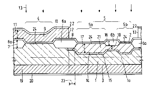
~ig. 1 shows a semiconductorbody 1, which may
¦ consist, for example, mainly of p-type silicon having a ~,
¦ resistivity of about 10 Q cm. The starting material may
be a homogeneously doped mono-crystalline sili~on wafer,
of which the major surface 2 is preferably a (100) ~~~
surface. A silicon wafer may also be used consisting of a '~
~ more highly doped substrate on which a more weakly doped
! epitaxial layer of sufficient thickness is situated. The
~ ~ 30 circuit elements of the integrated circuit are then
! mainly provided in this epitaxial layer. This possibility
is shown diagrammatically in Fig. 1 by the dot-and-dash
line la representing the interface between the substrate
and the epitaxial layer.
The semiconductor body 1 can be provided in a
usual manner at the major surface 2 with a first pattern
of field insulation 6a. This pattern of field insulation
.'~
~ :
PHN 11.440 8 ~ ~ 3 3 6 4 810.6.1986
6a has a first thickness 7 and limits, viewed on the major
surface 2, one or more active regions 4, 5. The active
region 5 in this example has two parts 5a and 5b,
between which an insulating region 6b is situated, which
is integral with the pattern of field insulation 6a,
but has a smaller thickness 16.
A masking 8, 9, 10 with a second pattern can
now be provided on the semiconductor body with the insula-
ting regions 6a and 6b. This masking has one or more
openings 12 indicated by their edge, which are situated so
that through each opening 12 at least part of the said one
or more active regions 4,5 are accessible for doping. In
the present example, the active region 5 is concerned,
which as a whole lies within the opening 12. An implanta-
tion treatment is then carried out at a given energy,
which is indicated by the arrows 13. The term "implanta-
tion energy" is to be understood to mean, as is usual, the
product of the number of electron charges per ion and the
acceleration potential.
The masking 8, 9, 10 has a layer 9 provided with
the op~ings 12 and consisting of a semi-masking material
for the ions used in the implantation treatment. The layer
I 9 has a second thickness 11. The implantation energy is
¦ chosen to be so high that in the part 5a, 5b accessible
25 for doping of the said one or more active regions 4~ 5, $he
penetration depth 17 of the dopant is at least substantially
equal to the first thickness 7 of the field insulation 6a.
Under the insulating region 6b, the accelerated ions
penetrate to a smaller depth 18 into the semiconductor
30 material of the semiconductor body 1 due to the fact that
the ions have to penetrate in situ through the insulating
; region 6b and then lose part of their energy. If, for
example, phosphorus is implanted, a continuous n-type
region 21 can be obtained, which is separated by a pn
junction 15 from the remaining part of the semiconductor
~ body 1. This n-type region 21 may serve, for example, as
3 substrate region of a p-channel field effect transistor to
,.
-
PHN 11.440 9 1 3 3 0 6 4 & . 6.1986
be provided therein or as collector or emitter region of
a bipolar npn transistor. In the part 5b, for example,
a substrate contact or a collector or emitter contact or,
for example, also a second transistor may be provided.
The layer 9 provided with the openings 12 and
consisting of semi masking material is a second comparati-
vely thick layer of a second material, which is provided
on a comparatively thin first layer 8 of a first material
forming also part of the masking 8, 9, 10, the first layer
8 covering at least those parts of the surface of the
semiconductor body 1 which correspond to the openings 12
in the second layer 9. The first and second materials are
relatively different materials. The third layer 10 of the
masking 8, 9, 10 is a comparatively thin layer of a third
material, which is situatedon the second layer 9. This third
layer 10 has one or more further openings 22, each further
opening 22 corresponding to one of the one or more
openings 12 in the second layer 9. The third material
differs from the second material.
In a preferred embodiment of the method according
to the invention, a masking 8, 9, 10 is used, of which the
firt layer 8 is a silicon nitride layer having a thickness
1 of, for example, about 0.1/um and of which the second layer
¦ 9 is a polycrystalline or amorphous silicon layer having a
thickness of, for example, about 1.5/um, whi~e the
third layer 10 is a thin silicon oxide layer which may be
obtained, for example, by thermal oxidation of the silicon
layer 9 and which has a thickness of, for example, about
0-2/um-
Before the advantages and the further details of
the first example of the method according to the invention
are disclosed, first the terms "penetration depth" and
~1 "semi-masking material" will be further ex plained.
In the present description, the terms "penetration
depth" and "average penetration depth" are used synonymous-
ly and side by side. Both terms have the same meaning in
this description and are generally designated by "range".
~`
PHN 11.440 10 1 330648 lo.6.1986
During the implantation of accelerated ions in a body
or layer of a given material~ the term "penetration depth"
or "range" is to be understood to mean the distance of
the area in the body or the layer at which the concentra-
tion of the implanted material has a maximum from thesurface ofthe body or the layer, through which the
accelerated ions have penetrated into the body or the
layer. The concentration distribution of the implanted
material around the concentration maximum can be
characterized in usual manner by a spread 6 . The
penetration depth generally depends inter alia upon the
size of the ions, upon the acceleration energy and upon
the relevant material.
Many of the materials usual in the semi-conductor
technology, such as silicon, silicon oxide, silicon
(oxy)nitride, but also the conventional photo-lacquers
(resists) have a comparable penetration depth by
accelerated ions. This means inter a _ that often implan-
tatinn can take place through thin layers of silicon
oxide or silicon nitride in the subjacent semiconductormaterial. Another consequence is that layers of such
materials can be used as a masking layer during implan-
tation treatments only as far as the layer thickness is
chosen to be sufficiently large to obtain the desired
masking effect. This in contrast with many metal layers,
such as layers of molybdenum or tungsten or other not too
light metals. The penetration depth of these materials is
generally much smaller than the penetration depth of
silicon so that metal layers often form a good masking
even if they are comparatively thin. In order to distin-
guish them from satisfactorily masking materials, such
as heavy metals, the aforementioned materials, such as
silicon oxide, are designated as !'semi-masking" in the
present description. In general the class or group of
semi masking materials comprises the materials having for
the same accelerated ions and the same implantation energy
a penetration depth which is comparable with or is at least
-
~ ,
PHN 11.440 11 1 3 3 0 6 4 8 1 o. 6.~1986
substantially of the same order as the penetration
depth of the material of the body in which the accelerated
ions have to be implanted. In other words: in maskings
consisting of a layer of semi masking material~ the
thickness of the masking layer will always be an
important non-negligible parameter, which can determine
whether the desired masking effect is or is not obtained.
In the present example, the openings 12 are
obtained by anisotropic etching of the oxide layer 10 and
the silicon layer ~, in which case a patterned photo-
lacquer layer (not shown) can serve in the usual manner
as a masking. This treatment can be carried out by means
of conventional plasma etching tech~4ues. The silicon
oxide of the third layer 10 can be etched selectively with
respect to the silicon of the second layer 9 and this sili-
con can be etched selectively with respect to the material
of the first layer 8. The presence of the first layer 8
within the openings 12 has the advantage that in situ
during etching any attack of the field insulation 6a, 6b
and any damage of the active semiconductor body are avoided
at least to a great extent. This first layer 8 preferably
comprises silicon nitnde.
Preferably, before, but otherwise after the
second layer is subjected to plasma etching, the photo-
lacquer layer is removed in a usual manner. After theopenings 12 have been provided, for example, an
implantation treatment is carried out, in which phosphorus
is implanted at a dose of about 3.10 per cm2 at an
implantation energy of about 800 keV. On the broken line
14, the concentration of the implanted phosphorus has a
maximum. The penetration depth 17 into the parts 5a
and5b of the active region 5 is about 0.5/um. If desired,
one or more implantation treatments may then be carried
out at a lower energy. For example, phosphorus may be
implanted at a dose of about 1.1012 per cm2 and an energy
of about 400 keV. By adaptation of the number of implan-
tations, the doses and/or the implantation energies,
:~,
..
i~ ~
~- -` 1 330648
PHN 11.440 12 ` 10.6.1986
suitable doping concentration profiles can be obtained
in the region 21. The number of subsequent treatments at
high temperature, the duration of these treatments and
the temperature at which they are carried out are further
also of importance for the doping concentrationprofile.
In such treatments, diffusion of the implanted doping can
in fact take place. Between the said implantation treatments
and/or after termination of these treatments, if
desired, one or more annealing treatments may be carried out
in a usual manner inter alia in order to restore any damage
and/or to activate the implanted doping,
In the present example, the pattern of field
insulation 6a is obtained in a usual manner by local oxida-
tion of the semiconductor body 1. A silicon nitride-
containing layer can then be used as an oxidation mask.The thickness of this masking layer is~ for example,
about 0 1/um. If required, under this masking layer a
further thin layer of silicon oxide or silicon oxynitride
having a thickness of, for example, about 40 nm may be
20 provided-
The oxidation mask covers the active regions 4and 5 entirely. As the case may be, an implantation
treatment for obtaining ~-type channel stopper zones may
subsequently be carried out, in which, if required, the
25 active region 5 and its immediate surroundings are covered
in a usual manner by a photolacquer pattern. After removal
j of the photolacquer pattern, a usual oxidation treatment is
carried out. After the oxidation treatment, the thickness
7 is, for example, about 0.6/um. The thickness 16 may be,
1 30 for example, about 0.4/um. After the oxidation treatment
j has been accomplished, the oxidation mask is removed
entirely. If required, a fresh thin silicon oxide layer 24
is provided on the active regions 4, 5. The thickness of
the layer 24 may be, for example, about 40 nm. Subsequent]y,
the layers of the masking 8, 9, 10 can be provided.
As far as the pattern of field insulation 6a is
not covered by the patterned layers 9 and 10 of the masking
..,-
.
~ 1 330648
PHN 11.440 13 10.6.1986
8, 9, 10, the phosphorus ions implanted at a high
energy penetrate through the field insulation 6a. The
concentrati~n maximum of the implanted dopant, which lies
approximately on the broken line 14, will be located in
situ about 0.3/um under the field insulation 6a. Under
the field insulation 6a, the surface concentration of the
doping at the interface between the n-type region 21 and
the field insulation may be about 1 to 3.1 ol 6 per cm3.
Provided that the distance 23, over which the concentra-
tion maximum at the outer edge of the active regiLn 5lies at a substantially constant depth under the inter-
face between silicon oxide and silicon, is not too small,
the said surface concentration offers a reasonable
protection against undesired channel formation so that a
channel stopper need no longer be provided. However, the
required distance 23 also influences the admissible minimum
distance between the active regions 4 and 5 and the circuit
elements to be provided therein. The distance 23 can be
reduced if the surface concentration in situ is increased,
As will appear, one of the advantages of the masking
8, 9, 10 resides in the flexibility, which becomes manifest
inter alia in various possibilities to be described below
of obtaining favourable doping concentrations under the
field insulation 6a without adversely affecting the
desired doping concentration profile in the active region 5
itself.
Under the thin insulation region 6b, the penetra-
tion depth 18 of the dopant implanted at a high energy may
amount, for example, to about 0,5/um. The surface concentra-
tion of the dopant will be under the insulation region 6babout 1 to 3.1 ol 6 per cm3.
After the implantation treatments have been
carried out 9 circuit elements can be provided in an
otherwise usual manner in the active regions 4,5 and/or
in layers to be formed in or on the semiconductor body 1.
Especially if insulated gate field effect transistors are
used in the semiconductor device, the quality of the
-
',~
PHN 11.440 14 1 330648 10.6.~86
semiconductor material in the active regions and of gate
dielectrics to be provided on these regions is of impor-
tance. nter alia in this connection it is advantageous
to use semiconductor material for the second layer 9.
Preferably, simultaneously with the second layer 9 of the
masking 8, 9, 10 a further layer 19 of semiconductor
material is provided on a second major surface 3 of the
semiconductor body 1 located opposite to the first-
mentioned major surface 2 and extending substantially
parallel thereto.
In the present example, before the second layer 9
and the further layer 19 are provided, the whole major
surface 3 is cleaned in a usual manner, during which
treatment, for example, oxide and/or nitride layers that
may be present are removed. During cleaning of the major
surface 3, the opposite active side of the semiconductor
body 1 may be covered by a protective photolacquer or wax
~ layer, which is removed after the treatment. Subsequently,
j the further layer 19 on the major surface 3 is directly
20 provided on the semiconductor mate~al of the semiconductor
body 1.
For the sake of completeness, it should be noted
that it is also sufficient that at least a substantial
part of the second major surface 3 is cleaned so that the
25 major surface 3 may be covered, for example near the edges
of the silicon wafer, by a protective layer during cleaning.
In a pref~red embodiment of the method according to
the invention, at least for the further layer 19 a semicon-
ductor material is used having a comparatively high
concentration of a dopant. T~his dopant can be incorporated
in a usual manner during the step of providing the second
and further layers 9 and 19, respectively. The further
layer 19 or both layers 9 and 19, after they have been
formed, may be doped in a usual manner, for example from
the gaseous phase, in which case PH3 may be used.
Preferably, a protective layer 20 is provided on
the further layer 19 of semiconductor material. This layer
~ ,, . . :.
l ~
~`:
t 330648
PHN 11.440 15 10,6,1986
may be9 for example, a silicon oxide layer, which may be
provided simultaneously with the third layer 10. The third
layer 10 may also be provided before the doping is
introduced into the further layer 19 and the protective
layer 20 may be provided after this doping treatment.
Due to the provision of the further layer 1g, it
is possible to carry out a getter treatment at any desired
instant during the further process of manufacturing in a
usual manner. A great advantage resides in the fact that
implantation treatments at a high energy are generally
carried out at comparatively early stage of the whole
manufacturing process so that with the use of the method
according to the invention, the means for obtaining a
good getter effect are present on the semiconductor body 1
already from this early stage of the manufacturing process.
For example, it is favourable that alrea-!-iy before gate
dielectrics for field effect transistors are grown or
applied, a getter treatment can be carried out. This may
have a favourable effect on the quality of the semiconduc-
tor material in the active regions and of the gatedielectric. In general, after the implantation treatment
at the given high energy, a getter treatment is
advantageously carried out before one or more doping
treatments for obtaining semiconductor zones of circuit
elements. For example, the aforementioned annealing
treatment(s) and the said getter treatment may be carried
out wholly or in part simultaneously as a combined treat-
ment. During the getter treatment, the semiconductor body 1
is heated, for example, for about 15 minutes in an inert
atmosphere at a temperature of about 925C, after which
cooling takes place in a usual manner.
The third layer 10 of silicon oxide in this
example serves inter alia to obtain a good adhesion of
the masking photolacquer layer used during etching of the
openings 22 and 12. As the third layer 10, another
dielectric material may also be used. The use of the third
layer also affords the advantage that the openings 22 can
~ `' .
.
,~
1 330648
PHN 11.440 16 10.6.1986
be provided with great accuracy in this comparatively
thin third layer and that furthermore, due to the favourable
masking properties of the third layer, an accurate image
of the openings 22 can be obtained in the second layer 9
during plasma etching of the openings 12.
The ~hird layer 10 can be removed before or
after the implantation treatment carried out at a high
energy, Furthermore, the silicon nitride of the first
layer 8 is removed from the openings 12 before or during,
but preferably after the removal of the third layer 10.
In the last-mentioned embodiment, the pattern of fields
insulation 6a cannot be attacked during removal of the
third layer 10.
This is especially of importance if the
pattern of field oxide 6a consists wholly or in part of
the same material as the third layer 10. The silicon nitri-
de is preferably removed from the openings 12 only after
the said implantation treatment. Subsequently, the second
layer 9 can be removed. The active region 5 is then still
protected by the thin silicon oxide layer 24. In a
simplified and further schematized form, the semiconductor
body 1 can be represented at this stage of the manufac-
turing process as in Fig. 2.
Whilst using the remaining part of the first
layer 8 as a masking, which was obtained from the masking
8, 9, 10 without a further photolithographic treatment
being required, for example, a further implantation treat-
ment may now be carried out. For example, boron may be
implanted in order to adjust the threshold voltage of a
` 30
~-channel field effect transistor to be prov ded in the
active region 5. The dose can be about 1.10 per cm
and the implantation energy may be about 25 keV. If
required, before this implantation treatment, the oxide
layer 24 may be removed from the active region 5 or may be
replaced by an oxide layer having an aocurately defined
thickness.
After removal of the remaining part of the first
.~
P~ 11.44~ 17 1 3 3 0 64 8 10.6.1986
layer 8, one or more implantation treatments may
be carried out in the active region 4, in which case,
if required, the active region 5 may be protected, for
example, by a photolacquer mask.
If an implantation treatment has also to be
carried out at a high implantation energy in the active
region 4, for example, if the remaining part of the
first layer 8 is still present, a fresh second layer 9
of semiconductor material and a fresh third layer 10
may be provided. Subsequently, as already described above,
openings 12 and 22 are provided in these layers 9 and 10,
these openingsbeing this time situated above the active
region 4 (Fig. 3). In this variation of the masking
8, 9, 10, the first layer 8 is not a fully continuous la~er,
but this first layer 8 covers at least those parts of the
surface of the semiconductor body 1 which correspond to
the openings 12 in the second layer 9. Through the openings
12, for example~ boron may be implanted comparatively
deeply in the semiconductor body 1.
- When by one or more implantation treatments
also the doping concentration profile of the p-type
doping desired in the active region 4 has been obtained in
this region in the same manner as described for the active
region 5, the layers 8~ 9 and 10 of the masking have be~
removed and a getter treatment has been carried out, the
semiconductor body 1 is prepared to such an extent that
field effect transistors can be further provided in a usual
manner in the active regions 4 and 5. For illustration and
~ by way of example, one of the possibilities for the
;~ 30 further procedure of the manufacturing method will be shown
hereinafter
As far as the silicon oxide layer 24 is still
present, it is removed and a fresh oxide layer is provided
by thermal generation, which layer serves as a gate
dielectric 25. The thickness of this silicon oxide layer
may be 3O to 5O nm. Over this oxide layer, a polycrystalli-
ne or amorphous silicon layer having a thickness of about
~. .
, .
PHN 11.440 18 1 330648 lo 6.l986
0.6/um can be provided by deposition from the gaseous
phase at low pressure (LPCVD). This silicon layer is doped
from the gaseous phase by means of PH3 with phosphorus and
is provided with a silicon oxide layer having a thickness
of about 50 nm by oxidation.
Subsequently, the upper oxide layer and the sili-
con layer can be patterned in a usual manner so that the
gate electrodes 26 and, as the case may be, also
conductor tracks 27 are obtained. If desired, a short
oxidation treatment may then be carried out in order also
to cover the vertical walls of the gate electrodes 26 and
the conductor tracks 27 with an oxide layer. The silicon
tracks 26 and 27 are then fully enclosed by the oxide layers
28, 25 and 6a, respectively. A photolacquer layer 29 is
then deposited and provided with a pattern. Whilst using
this photolacquer layer 29 as a masking, a doping for
source and drain zones 30 and contact zones 31 for n-
type regions 21 can be provided. For example, arsenic
is implanted at a dose of about 5.1 ol 5 per cm2 and an
implantation energy of about 40 keV. Fig. 4 shows
diagrammatically the semiconductor body 1 at this stage
of the manufacture.
Subsequently, the photolacquer masking 29 is
replaced by a photolacquer masking for providing the
doping for p-type source and drain zones 32 and for contact
zones 33. For example, as a dopant boron is implanted at
a dose of about 3.10 5 per cm2 and an implantation energy
of about 16 keV. The photolacquer masking is then removed
and a silicon oxide layer 34 having a thickness of about
0.5/um is deposited. An annealing treatment can then be
carried out, in which the semiconductor body 1 is heated,
for example, for 30 to 60 minutes at a temperature of about
650C. This treatment may also be carried out in part
(for examplefor about 15 minutes) at a higher temperature
of about 925C, cooling then taking place in a usual manner
so that a getter effect is also obtained.
When contact openings have been provided in the
.
.
1 330648
PHN 11.440 19 10.6.1986
^xide layers 34, 25 and 28, a conductive layer of,
for example, aluminium can be deposited and be provided
with a pattern by etching. If required, a barrier layer of,
for example, tungsten or titanium may be provided under the
aluminium. Furthermore, silicide may be provided or formed
in the contact openings before the aluminium is deposited.
Thus, the semiconductor device is provided with conductor
tracks 35 for electrical connection and electrical
interconnection of the circuit elements (Fig. 5). If
desired, the semiconductor device may also be provided with
one or more further layers of conductor tracks (not shown),
which are separated by further insulating layers (not
shown) from each other and/or from the layer of conductor
tracks 35. Furthermore, the al~tive side of the semiconductor
body 1 of the semiconductor device may be covered sub-
stantially entirely by a protective insulating layer (not
shown) of, for example, silicon nitride. Finally, the
silicon wafer can be subdivided in a usual manner into
separate integrated circuits and these integrated circuits
can be finished in a usual manner in a conventional
envelope,
The layers 19 and 20 on the major surface 3 are no
longer required after the last getter treatment and may be
removed, if desired, after this treatment. However,
the removal of these layers is not necessary.
In the first example, the pattern of field
insulation 6a is obtained by local oxidation of the
silicon body 1. Such a pattern may also be obtained in a
different manner, however. For example, in a variation of
the first example, first the silicon wafer 1 is provided
t~ '
with an etching mask, which consists, for example, of a
layer 40 of silicon oxide, which is patterned by means of a
photolacquer mask 41 (Fig. 6). The etching mask 40 covers
the active regi~ns of the semiconductor device. After
removal of the layer 41, grooves having a depth 42 of, for
example, about 0.8/um are provided in the semiconductor
body 1 by plasma etching. This groove depth can advantage-
~`3
..
~.
:
:~` ~
~:
~,
:~ ,.
-`-` 1 330648
PHN 11.440 20 10.6.1986
ously be chosen so that the line 14 of maximum concentra-
tion in the semiconductor ~ody 1 under the ultimate
field insulation extends immediately under the interface
between the semiconductor material and the field
insulation, If desired, for example, boron may be implan-
ted in the walls of the grooves or in parts thereof for
increasing the surface concentration in situ. The walls of
the grooves can be provided with a silicon oxide layer 43
having a thickness of about 50 nm, after which a layer 44
of si~con nitride can be deposited having a thickness of
about 0.1/um (Fig. 7). Subsequently, a layer 45 of
polycrystalline or amorphous semiconductor material or
of silicon oxide can be deposited. The thickness of the
layer 45 can be about 1/um. Planarization can then take
place in a usual manner, in which case, for example, a
photolacquer layer 46 may be used. When etching back
the layers 46, 45, this treatment can be stopped when the
silicon nitride situated on the active regions has been
reached. If the layer 45 consists of semiconductor
material, the etching can be continued, whereupon the
semiconductor material in the grooves can be oxidized in
such a manner that the grooves are then completely fi~ed
again. After the silicon nitride 44 and the silicon oxide
43 have been removed from the active ~gions, a fresh
¦ 25 si~con oxide layer 24 is formed on the active regions
¦ (Fig. 8). The semiconductor body 1 is now provided with a
¦ pattern of field insulation 6a, which mainly consists
of the still remaining parts of the layers 43~ 44 and 45.
Subsequently, the masking 8, 9, 10 can be
provided in the manner already described and the further
processing steps already described may also be carried
~ out, as far as necessary. In Fig. 8, the semiconductor
j body 1 is shown at the same stage of the manufacture as
that to which the invention relates.
In the second example, the semiconductor body 1
is also first provided in a usual manner with a pattern
of field insulation 6a. Subsequently, the layers of the
,,:"
, : ,.: ~, ~ :. ~ ~ : . - ' ' ~ :
,,~
, , '
..
- PHN 11.440 21 1 3 3 0 6 4 ~o. 6.1986
masking 8, 9, 10 are provided. After a photolacquer pattern
has been provided on the third layer 10, the layers 10 and
9 are etched~ a suitably chosen combination of
isotropic and anisotropic etching being used at least
5 during etching of the layer 9 so that openings 12 having
oblique edges are obtained. Etching methods in which ob-
lique edges are obtained are described in the technical
literature. Examples thereof can be found in Solid State
Technology, August 1982, p. 98-103, and in Journal Vacuum
Science and Technology B, Vol. 3, No. 1, Jan.-Feb.1985 p.
15-19. If required, after the layer 9 has been etched,
the openings 22 in the layer 10 are enlarged, for example,
by under-etching of the photolaquer pattern, orthe third
layer 10 is entirely removed (Fig. 9).
The use of a semi-masking layer 9 provided with
openings 12 having o~lique edges, as shown in Fig. 9, has
the advantage that after the implantation treatment at
high energy the line 14 of the maximum concentration of
the dopant under the oblique edges of the openings 12
intersects the interface between the semiconduct~r
material of the semiconductor body 1 and the adjoining
material of the pattern of field insulation 6a. As a
result, in the immediate proximity of this intersection
of the line of maximum concentration and the said inter-
face, a comparatively high threshold voltage for
parasitic channel formation and hence a comparatively
satisfactory channel stopper effect is obtained.
In a variation of the second example, there is
first etched isotropically for some time until the remai-
ning layer thickness 36 of the second layer 9 in the
openings 12 is just so large that the accelerated ions to
be used for implantation still can reach the semiconductor
material of the semiconductor body 1 throlgh the remaining
part of the second layer 9 and the pattern of field insula-
tion 6a (Fig. 10). The last part of the openings 12 is then
etched anisotropically. After removal of the third layer
10 (Fig. 11), the implantation treatment is carried out.
, -
....
, : ..~ . ,.
., ;: `~ ' . ` ~. - ~. ` ' . : : . .
PHN 11.44O 22 1 3 3 0 6 4 8, o . 6.19~6
The line 14 of the maximum concentration will
extend in the semiconductor body 1 at the edges of the
region 21 over a certain distance (the part 37)
substantially parallel to and immediately under the
interface between the semiconductor material and the
pattern of field insulation 6a. As a result, a further
improved channel stopper effect is obtained.
In the third example, a second layer 9 having
a thickness 11is used which is chosen so that the overall
thickness of the second layer 9, the first layer 8 and the
pattern of field insulation 6a is so large that the line
of maximum concentration 14 extends after the implantation
treatment under the field insulation 6a in the semi-
c~nductor material immediately under the interface with the
~ 15 field insulation and substantially parallel to this
¦ interface. The relevant part of the line 14 is denoted
in Fig. 13 by reference numeral 37. The third layer 10
in this example consists of a satisfactorily masking
material, such as molybdenum or tungsten. A ~urther layer
38 of,for example, silicon oxide and/or photolacquer is
provided on this third layer 10. Openings having the same
size as the openings 12 are first provided in the layers
38, 10 and 9 (Fig. 12). Subsequently, the enlarged
openings 22' are provided in the layer 10. The openings
22' are therefore derived from the same original pattern as
the openings 12. The openings 22' are larger than the
openings 12, but further correspond entirely to these
openings 12. The layer 38 is then removed. Subsequently,
the implantation treatment can be carried out (Fig. 13).
Also in this example, the optimum channel stopper effect
can thus be obtained under the field insulation 6a~ which
can be realized without a specific and additional implan-
tation treatment being carried out.
It will be appreciated that in the third example
the second thickness 11 of the second layer 9 is too small
to obtain a substantially complete masking of the implan-
ted dopant. In this example, this substantially complete
~,'`'
~"~
. - ~" : .
~' ~
-- ` 1 330648
PHN 11.440 23 10.6.1986
masking of the implanted dopant. In this example, this
substantially complete masking is guaranteed by the use
of the third layer 10 of satisfactorily masking material.
In the examples, in which the masking 8, 9, 10 comprises
only layers of semi-masking material, the overall thick-
ness of the layers is invariably chosen so large, however,
that outside the openings 12, 22 a substantially complete
masking is obtained. In this connection, the second thick-
ness 11 of the second layer 9 is preferably larger than
the first thickness 7 of the pattern of field insulation
6a.
In the fourth example, a layer 8 of silicon
nitride, a layer 47 of amorphous or polycrystalline
silicon, a layer 48 of silicon oxide or silicon nitride,
a layer 49 of amorphous or polycrystalline silicon and a
layer 10 of silicon oxide or silicon nitride are formed on
the semiconductor body 1, which is already provided with
the pattern of field insulation 6a. The layers 47, 48 and
49 together constitute the layer 9 of semi-masking material
Openings 22 are first provided in the layer 10. The layer
10 then serves as a masking during etching of openings 50
in the layer 49 (Fig. 14).
Subsequently, a layer of, for example, silicon
oxide can be deposited, which is then removed aniso-
tropically without a masking~ for example by plasma
etching, in such a manner that a part 51 is left along the
edges of the openings 50 (Fig. 15). If the layer 48
consists of a material masking against oxidation, the edge
portion 51 can also be obtained by oxidation of the layer
49. If the layer 10 then also consists of a material
masking against oxidation, the said oxidation treatment is
sufficient. Preferably, the layer 10 is first removed
(but without the part ofthe layer 48 exposed in the
openings 50 also disappearing) or this layer 10 consists,
for example, of silicon oxide. In this case, after the
oxidation treatment of the layer 49, the oxide present is
etched back anisotropically until practically only the
edge portion 51 is left.
;
. ~
PHN 11.440 24 1 3 3 0 6 4 8 1 o . 6.1986
Openings 53 are then etched in the layer 47, the
exposed part ofthe layer 48 first being removed if this
exposed part has not yet been etched away during the
preceding processing steps. ~he thickness 52 of the sub-
layer 47 in this example is chosen to be substantiallyequal to the thickness 11 of the layer 9 in the example
shown in Fig. 13. In the present exa!~ple, the thickness 11
of the second layer 9 composed of the sublayers 47, 48
and 49 is further larger than the sum of the thicknesses 7
and 52 of the pattern of field insulation 6a and the
lower sublayer 47, respecti~ely. This thickness 11 is
moreover chosen so large that outside the openings 22, 5O
a substantially complete masking of the implanted dopant
is obtained with the masking 8, 9, 10. This thickness 11
is preferably at least equal to the penetration depth 17 of
the dopant in the part ofthe active regions located within
the openings 12 and accessible for doping.
Subsequently, the edge portions 51 can be removed.
If the layer 10 and/or the layer 48 consist of the same
material, the layer 10 and/or the part ofthe layer 48
covered first by the edge portions 51 will disappear
simultaneously. If the layer 10 and/or the layer 48
consist of a different material, a further etching
treatment can be carried out before or after the implanta-
tion treatment at high energy, in which further etchingtreatment the exposed part of the layer 8 may also be
removed simultaneously.
Fig. 16 shows the semiconductor body 1 after the
implantation treatment. The openings 5O and 53 in the
layer 49 and the layer 47, respectively, together constitute
the openings 12 in the layer 9 of semi masking material,
which have a stepped profile. As a result, a doping
concentration profile is obtained which is comparable with
¦ that of the example shown in Fig. 13. The line 14 of
maximum concentration of the doping extends over a distance
37 accurately defined by the stepped profile of the
opening 12 immediately under and substantially parallel to
33n648
PHN 11.440 25 10.6.1986
the interface between the pattern of field insulation 6a
and the semiconductor material of the semiconductor body 1.
When comparing the third and fourth examples, it
appears that the intermediate layer 47 of the fourth
example may be replaced by the satisfactorily masking third
layer 10 of the third example. The layer 10 ofthe fourth
example, which then no longer serves as the third layer of
the masking, and the sublayer 49 are then auxiliary
layers which serve to realize in an accurate manner the
openings 12, 22' shown in Fig. 13.
If in the fourth example the getter layer 19
(not shown) is present on the back side of the semiconductor
body 1, this layer 19 can be provided simultaneously with
the sublayer 47 and/or simultaneously with the sublayer
15 49.
In the examples described, especially the second
¦ layer 9 will have a sufficiently large thickness to be used
t as a lift-off masking. For example, a comparatively thin
layer of molybdenum or another suitable material may be
20 vapour-deposited in a direction substantially at right
angles to the major surface 2 of the semiconductor body 1.
Subsequently, the layer 9 can be removed, the part of the
vapour-depsoited molybdenum layer present thereon then also
disappearing. Thus, a molybdenum pattern is obtained which
25 forms an accurate image of the openings 12. Where openings
12 were present, the surface is covered ~ith molybdenum,
~ whereas no molybdenum is present on the remaining part
; of the surface. This molybdenum pattern may be used, for
example, as a masking during further desired treatments of
30 the semiconductor body. If in the example shown in Fig. 13
before the vapour-deposition of the said molybdenum layer
1 the openings 22' are used to selectively remove the part of
the layer 9 exposed within these openings, the ultimate
molybdenum pattern accurately covers the doped regions 21.
35 In a similar manner, in the example shown in Fig. 16, whilst
using the sublayer 49 provided with openings 50 as a
masking, the exposed part of the sublayer 47 can first be
'
',
l ~
: ~ :
~, . ~
r ., ,~
--- 1 330648
PHN11.440 26 10.6.1986
removed Also in this case~ the molybdenum pattern will
cover accurately the doped regions 21.
In all examples, the first layer 8 protects
the underlying semiconductor body during the step of
providing the openings 22 and/or 12. In this connection, an
important advantage is obtained if the first material of
the first layer 8 differs from the material from which
the pattern of the field insulation 6a is formed at least
for the major part. Generally~ the last-mentioned
material will be silicon oxide. In the example shown
in Fig. 8, this main component of the pattern of field
insulation 6a may also be a semiconductor material. As
the first material use is preferably made of silicon nitri-
de. The use of this material affords the great advantage
that the further materials used for the layers 9 and 10,
47, 48 and 49 and the edge portions 51 need not be
selectively removable with respect to the material of
the pattern of field insulation 6a. Especially for the
layers 10 and 48 and for the edge portions 51 silicon
oxide can then be used. The relevant silicon oxide can
in fact be etched away without the pattern of field
insulation 6a covered by the first layer 8 being
attacked.
Only for the first example the manner is
described in which the manufacturing process can be
continued and accomplished after the implantation treatment
at high energy. The further examples described of
the method according to the in~ntion may be accomplished
in a similar manner or in a different known manner. It
is then especially decisive what circuit elements
have to ~e realized.
The present invention is otherwise not limited
to the embodiments described. Within the scope of the
invention many variations are possible for those skilled
in the art. ~or example, semiconductor materials other
than silicon, such as germanium or AIIIBV compounds,
may be used. If the third layer 10 comprises a layer of
..,
~,. ~ .. .. :
~' ~
" -
.
1 330648
PHN 11.440 27 10.6.1986
silicon oxide, the latter may be formed instead of by
thermal generation, for example, also by deposition. This
also applies, for example, to the layers 20 and 43. It is
not necessary to provide a doping up to a high concentration
in the layer 19 to obtain a getter effect. Furthermore,
in the examples shown in Figures 9 to 16, a layer 19 may
also be provided on the back side of the semiconductor
body 1. This layer 19 may be provided simultaneously with
the layer 9~ the sublayer 47 and/or the sublayer 49.
For the sake of simplicity, in most of the
examples the influence of the presence of thin layers
within the openings 12 on the penetration depth of the
implanted doping in the semiconductor material of the
semiconductor body 1 is neglected or is at least left
15 out of consideration. It will be appreciated that, espec-
cially if be~orehand an accurate estimation of the
resulting doping concentration profile is desired, the
influence of all the layers located within the openings
12 as to their thickness and their specific penetration
20 depth (stopping power) has to be taken into account.
In the examples, the first material of the first
layer 8 differs from the second material of the second
layer 9 and the latter material in turn differs from the
third material of the third layer 10. If the second layer 9
25 is comp~ised of a number of sublayers, as in the example
shown in Figures 14 to 16, an intermediate sublayer may be
used, which consists of the same material as the third
layer 10 or of the same material as the first layer 8.
Although this is not necessary, the first material
30 preferably also differs from the third material.
~l In the example shown in Figures 14 to 16, at
least one of the sublayers 47 and 49 preferably consists of
semiconductor material. In this example, the thickness of
the sublayer 49 is not only chosen at least so that out-
35 side the openings 12 the desired practically whole masking
is obtained, but is also chosen so that edge por$ions 51 of
suitable dimensions can be obtained.
~ v . -~, ~
~ ~" ~
PHN 11.440 28 1 3 3 0 6 4 8 1 o . 6.1986
If the second layer 9 consists wholly or
in part of the same semiconductor material as the semicon-
ductor body 1 and/or the layer 45 and at least a part of
the second layer 9 has still to be removed at a stage at
which the first layer 8 does not form a continuous layer,
the semiconductor material of the semiconductor body 1
and/or the layer 45 is preferably covered by a protective
layer, such as the layer 24, which is provided before the
first layer 8 of the masking 8, 9, 10 was provided.
10 Preferably, this protective layer consists of insulating
material which differs from the first material of the first
layer 8.
The masking 8, 9, 10 is preferably sufficiently
thick to obtain outside the openings of the second pattern
15 a practically complete masking of the implanted dopant. A
complete masking is not always necessary. If after the
implantation treatment at high energy the concentration
of the implanted dopant in the semiconductor material of
the semiconductor body 1 is small under the masking 8, 9,
2n 10 so outside the openings of the second pattern, with
respect to the ba kground doping concentration present or
with respect to doping concentrations to be provided later
in the relevant region of the semiconductor body 1, such a
non-complete masking will generally be admissible. Further-
25 more, the doping quantity obtained with a non-complete
masking under the masking 8, 9, 10 may be used, for
example, inter alia for the adjustment of the threshold
voltage of field effect transistors to be realized in
the relevant semiconductor region.
For each of the layers 8, 10 and 48, a suitable
choice may be made from materials, such as silicon oxide,
silicon nitride and aluminium oxide. For the third layer 10,
in general also a suitable metal, which in the examples
other than the example shown in Figures 12 and 13 need not
35 be satisfactorily masking, may be used. For the layer 49,
besides semiconductor material, oxide or, for example,
,.:
1 330648
PHN11.440 29 10.6~1986
polyimide may also be used. The layer 9 may also
consist of a suitable photolacquer. In this case, for
example, spin-on glass or aluminium, chromium or another
suitable metal may be used for the layer 10.
'
: -
"~
.~ ~., . . , ,, ~:: : . - .