Note : Les descriptions sont présentées dans la langue officielle dans laquelle elles ont été soumises.
1331866
METHOD AND APPARATU9 FOR ION ETCHING AND DEPOSITION
FIELD OF THE INVENTION
The invention relates to ion etchin~ snd ion assisted and
other deposition and more psrticularly to ion etchin~ existin~
surfsce topographies of objects to predetermined topographies in
accordance with an algorithm using image restoration and to an
ion source extraction grid apparatus providing selected ion beam
spatial distribution.
BACXG~iOUND OF THE INVENTION
Precision optical components having physical surface height
aberrations smaller than one wavelength of the incident radiation
are of strate~ic iuportance to the operation of Dany optical
syste-s. Such components are very expensive because of tho
enormous invest~ent of time snd sophisticated equipment required
to fabricate and figure their optical surfaces. Conventional
methods of fabricating and fi8urin8 optical surfaces involve
~rindin~ surfaces into optics usin~ abrasives. Althou~h modern
optic ~rinders have better abrasives, tools and even equipment
under computer control, the physical process is essentially the
~a~e as it has been for hundreds of years.
Ion etchin~, also known as ion sputterin~ and ion millin~
has been tried as an alternative process to abrasion. Ion
-.
sputteriny is a physical process in which an ion is caused to
impinge upon a surface of an object with sufficient energy to
cause atoms or molecules of the object to be liberated from its
surface.
~; I
.1 .
1331866
Sputtering has beco~e popular in the ~emiconductor industry.
However, sputtering hQs not found use in modifyin~ optical
~,surfaces because efforts to u~e ~putterin~ for optic ~urfacin~
were severely limited by the ion current from the ion sources
available at the ti~e. One type of ion source used in such
atte~pts is known as a Cockraft-Walton accelerator. U. S.
Patents 3,548,189 to Meinel et al and 3,699,334 to Cohe'n et al
illustrate such ion sources in their disclosed de~ices.
Cockraft-Wslton as well as other ion accelerators used in such
attempts are onlr capable of drivin~ a maximu~ bean current of a
few hundred microamperes and produce quite hi8h ion energies,
,; often a fraction of an MeV. Linitations result iron tho
~I funda-ental ,desi~n of ~uch ion source~. For exa~ple, sucb
sources contain only a sin~le sperture for ion extraction. The
ion current extractsble fro- a sin81e aperture is proportional to
the volta~e applied to the aperture which in turn deteraines the
ion ener~y. The use of a sin~le aperture as in the prior art
thus sndates that hi~h ~olta~e be applied to the ion extraction
i' aperture which results in hi~h ener~y ions in order to obtain an
~ ion current on the order of a hundred aicroampere~. Due to such
,,
li~itation~ ion bea~ etchin~ has been ossentially unworkable.
In the late 1970's the ~aufman ion source as disclosed in
~ the publication, Technology of Ion aeam Source~ Used in
¦ - Sputterin~, Journal of Vacuum Science and Technolo~y, Vol. 1~, pp
l 272-276, March~.~pril 1978 by H. R. Kauf~an et al was developed.
¦~ ~ The ~aufman ion source i- capable of producin~ beam currents of a
¦ lar~e fraction of an aopere, at ener~ies within the 300-1SOO eV
I:
! ;~ 2
.
.
- 13318~6
range. The beam i~ sufficientlr controllable, stable and
repeatable, to be sati~factory for use in qurface modification
device~. A Kaufman ion ~ource having a grid ~tructure in
accordance uith the invention can produce minimum current levels
of at lea~t about 200 times and optimally about 800 to 1500 times
the current level of the Cockraft-Walton and other devices u~ed
previouslr in ion etching. Such Kaufman ion source beam current
i~ on the order of 30 to 400 mA ver~us a Cockraft-Walton device
besm current of less than 0.3 mA.
The ions usecl in the 3,548,189 device are of subQtantially
the same ener~y and a uniform current density i9 necegQarr. Onl~
narrow ion bea- sources are used and selective deposition in
combination with selective removal is not pos~ible. Such devices
are limited to the figurin~ of small diameter element~ because
bean deflection is uaed as the steering mechani~m, the ion source
not being translatable, i.e., movable. For lar~e diameter
optics, such as those havin~ diameters on the order of one-half
meter or more, the distance froD the deflection plates to the
surface would have to be near the diameter of the -~urface. Beam
current loses due to residual ~as in the chamber would be ~reat
and make the proces~ very inefficient. Too, beam dwell pattern
computation i~ not considered in such prior art device~ and
methods usin~ i-a~e proces~in~ and srstems theory for optimized
material removal are not applied.
In device~ such as that ~hown in U. S. Patent 3,699,334, ion
beam impin~ement control is limited to electroQtatic and magnetic
~ 3
'- . ' ' : : ' - :~ ,, - -
1 33186~ 74389~11
deflectlon of the beam and to rotation of the ob~ect to be etched.
In practlslng the lnventlon the lon source 18 ltself moved. The
lon sources used ln the prlor art are elther constructed as an
lntegral part of the vacuum system contalnlng the ob~ect to be
etched or they are external to the vacuum system and connected
thereto by a tube whlch ls evacuated wlth the vacuum system. No
such prlor art systems utlllze translatable lon sources. Too, the
lon beam ls necessarlly malntalned contlnuous~y ln such prlor art
devlces ln part because of the hlgh voltages lnvolved ln extract-
lng 20 keV to 100 keV lons. Dwell computatlons are based on a two
step method ln whlch the symmetrlcal errors need flrst be reduced
to zero. Then lsolated symmetrlcal errors are removed. In prac-
tlslng the lnventlon all errors, symmetrlcal and nonsymmetrlcal,
are removed ln one step. Nonsymmetrlcal and arbltrarlly shaped
beam ob~ects can not be flgured wlth such prlor art devlces. In
additlon the beam energles of the prlor art devlces, 20 to 100
keV, are known to damage many materlals. The apparatus of the
lnventlon operates at a maxlmum energy of about two keV. The
prlor art beam taught by the '334 patent only focuses the lon beam
to a dlameter between one and flve mllllmeters whereas that of the
lnventlon focuses the lon beam wlthln a two to flve centlmeter and
larger range to enable the correctlon of a wlde range of slzes of
surface aberratlons far more efflclently than wlth prlor art
devlces. The lon source used ln accordance wlth the inventlon
provldes electrons to avold the electrlc charge effects requlrlng
a separate source of electrons ln prlor art devlces.
E -
.
133186~
Thus, it can be seen that the prior art devices and methods
can not figure lar~e surfaces and can not use both removal and
deposition to figure a surface Such de~ices are limited to lou
current, hi~h ener8y, narrow beao ion sources and there i~ no
control of beao current spatial distribution Large and non
symmetric surfaces can not be etched by such devices and methods
SUMMA~Y OF THE INVENTION
In accordance with the invention, there is provided a method
and apparatus for etching a selected surface of an object from
its existin~ topo~raphy to a predeter~ined topography by
comparin~ the exiitin~ topo~raphy to the predeter~ined topo8raphy
and usin~ an al~or;thu co-prisin~ ima~e restoration and an ion
bea- to selecti~ely re-ove aterial frou the surface Tho
al~orith~ ay also control deposition to deposit aterial on the
surface to reach the predeter~ined topo~raphy The ai~orith~
comprises the use of nonlinear windowin~ techniques followed by
an ima~e restoration step to ~enorate a bea~ dwell array which
will yield tho desired or predeteruined topo~raphy The oethod
can be used to provide nonsYanetric as well a~ sy-oetric surface
topo~raphy and to deteraine uhether an existin~ surface
topo~raphy is ~uitable for etchin~ or deposition in accordance
uith preselected citeria The ion beam used is prefeiably hi8h
current, low ener~y and broad Surface extrapolations ~ay be
used to a~oid ed~e effects Hi~h curvsture and complex surfaces
uay bo formed An ion source ~rid apparatus for extracting ions
fro- a plas~a source in accordance with the invention co~prises a
sheet of nonconductin~ ~acuuo compatible oaterial, such as a
,;~
~ "~" S
1 33186~
ceramic, having conductive coatinBs on each surface. A plurality
of apertures penetrste the coatin~s and the sheet of material in
a predetermined pattern to provide an ion beam having a
preselected spatial distribution when a voltage is applied across
the coatin~s. The coatings may be disposed in a plurality of
correspondin8 discrete areas on each side of the sheet of
material, corresponding areas being provided with selected
voltages thereacross to provide an ion bea~ having a desired
spatial di~tribution. The voltages may be controllable to chan8e
to spatial distribution. The area and aperture patterns ~ay
comprise concentric circles about a central circular area.
One object of the present invention is to selectively etch
the surfaces of lar~e diaaeter objects.
Another object of the invention is to control ion beam
current spatial distribution.
Yet another object of the present invention is to use
selective aterial reaoval and deposition to fi8ure the surface
of an object.
Still another object of the invention is to provide
predeterained syrmetric and nonsymmetric surfaces.
Another object of the invention is to deternine uhich
objects are suitable for etching or deposition in accordance with
preselected criteria.
One advanta~e of the present invention is that in accordance
therewith, lar8e diameter optics and other elements can be
economically produced.
Another advanta~e of the pre~ent invention is that in
j 6
,;., ~ ~ . :- ~ - ,: '
, - - , . -
' ~
::-
., - . . -
.~ .. ..
~;
-:~ . .. , -;:
. . ...
.. :' . .
~ ~ :
133186~
accordance therewith a hi~h current, low energy, broad ion beam
can be used to etch a desired surface configuration on an object
Yet another advantage o~ the invention is that surface
extrapolations can be used to avoid ed8e effects.
Stiil another advanta8e is that high surface curvature and
complex surfaces can be figured.
Yet another advantage of the invention is that an object may
have its surface fi~ured, then evaluated for acceptabilitr, and
have subsequent operations such as thin film coatinB performed
thereon without the object bein~ removed fro~ a vacuum syste~.
Still another advantage is that delicate and lightweight
objeets can be fi~ured becsuse there is no wei~ht loadin~ on the
ob~eet in praetiein8 the invention as in eonventional ~rindin~ or
illing methods.
Additional objeets, advanta~es and novel features of the
invention will be set forth in psrt in the description which
follows, and in part will beco~e apparent to those skilled in the
art upon examination of the followin~ or car be learned by
praetiee of the invention. The objects and advanta~es of the
invention ~y be realized and attained br ~eans of the
instru entalities and eo~binations particularly pointed out in
the appended clai~s.
BRIEF DESCRIPTION OF THE DRAWINCS
The aeco~panrin~ drawin~s, which are incorporàted in and
form a part of the speci~ication, illustrate the invention, and
to~ether with the deseription, serve to explain the principles of
the invention. In the drawin~s:
.~ - .
~ 7
. .
~: ;
~ 1331866
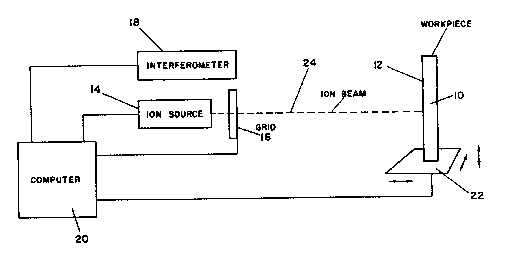
Fig. 1 illustrates a system for performing the method o~ the
invention;
Fig. 2 shows a cro~s section of an ion beam grit structure
representative of those of the prior art;
Fi~s. 3A and 3B are cros~ sectional views of an ion beam
grid apparatus in accordance with the invention;
Fig. 4 illustrates an ion beam grid apparatus in accordance
with the invention having di~crete coating areas connectable to
separato volta~es;
Fig. 5 is a cross sectional view of the embodiment of Fi8. 4
schematically showing the discrete coating areas connected to
different volta~e source ;
Fi~s. 6A and 6B ~raphically depict ion beam spatial
.
distribution a~ it may be controlled by the embodiment of Figs 4
and 5; and
~Fi~s 7A and 7B show how ion beam spatial distribution may be
- predetermined by aperture placement in the embodiment of Fi~s 3A
and 3B.
DETAILED DESCRIPTION OF THE INVENTION
Re~erenoe is now made to Fi~. 1 which illu~trate~ a system
~uitable for carry~n~ out the method Or the invention. A~ seen
therein an object l0 having a surface 12, beam source 14, an ion
source ~rid 16 and an interferometer or other surface determinin~
or ~onitorin~ instrument 18 such as a phase measurin~
interferometer or heterodyne interferometer are po~itioned witbin
a ~acuum chamber lnot shown~. A computer 20 is operatively
connected to an apparatus 22 for controllin~ the po~ition of
.~ j 8
.,~,.-.. ' .- . .
: 133186~
object 10 Bes- source 14 and ion source 8rid 16 are al30 under
the control of computer 20 as is monitorin~ inqtrument 18 Ion
source 14 i~ preferably a Kaufman ion source such as disclosed in
a publication, Fundamentals of Ion-Source Operation by Harold R
Kaufman, Library of Con~ress Catalo~ Card Nuober 84-71750
~aufman sources are well known and produce hi~h current, low
ener~y broad ion bea~s containing nearly monoener~etic ions 80
that beac sputterin~ therewith is essentially a linear prooe~s
The renoval profile of the beam fro- source 14 i9 esscntially tho
same re8ardless of where on the surface 12 of object 10 beau 24
is directed Thus, sputterin~ yield remains constant Beam
source 14 and/or objeot 10 is translatable so that in operation
the be~ 24 re-ains nor-al, or at another selected fixed an~le,
to surface 12 or to a reference plane or surface The bea- 24
does not diver~e appreciably and its current ener~y distribution
renaina substantially constant durin~ operation Beaa source 14
ay additionallr couprise a sputter na~netron or other device for
ion assisted or other deposition
In accordanco with the invention an al~orith~ co~pares a
de-ired predeteruined surfaco topo~raphy with the existin~
sur~ace topo~raphy of surface-12 on object 10 and utilizin~
ima~e restoration, controls bea~ 24 to ion etch surface 12 to
produce the predeteroined surface topo~raphy The predetermined
topo~raphy may be sycnetric or nonsymcetric and ion assisted
deposition may be also used to fi~ure surface
In practicin~ the invention, ion etchin~ and ion depositin~
beac fi~urin~ is controlled usin~ deconvolution for nearly flat
l` ~ 9
:
1331866
optics, and matrix computations for optical and other elements
having large surface slopes and high curvatures. The ~odel for
figuring computation be~ins with the superposition integral,
/ (~ ,y )--d (2 ,y ) - ¦ ¦ t (a ,B )h (~ ,a ,y ,B )dadB ~ 1 )
where h~x,a,y,B) i~ the impulse re~ponse or point-spread function
for the srstem model. In this case the impulse is located at
point ~a,B). The function f~x,y) is the ori8inal surface profile
or existing topo~raphy of the optic or other element, and the
function d~x,r) is the desired surface profile or predetermined
surface topo8raphr. The function t~a,B) is the time that the ion
beam dwclls on the element at point ~a,B). The function
h~x,a,r,B~ is the aterial removal profile for the ion beam.
The material removal profile described as h~x,a,~,B) is
spatially variant. The shape of the removal profile can chan~e
depending on where the ion beam is pointed. If the removal
profile is fount not to chan8e with position, then the removal
profile is said to be position invariant or spatiallr invariant.
The removal function ar also have additional parameters related
to dynamicallr chan~in8 the mechanlcal and electrooa~netic
.
configuration of the ion source.
Figuring can also be performed by depositing material usin~
a deposition source. In this case the removal function is
replaced with an addition function which satisfies the same
constraints as the removal function. Those skilled in the art
will understand the calculations of the control parameters usin8
I
1~
'` 10
1331866
additi~e techniques, e.g., ion deposition, are the sa~e as the
calculations of the control para~eters for material removal,
e.~., ion etchin8-
For surfaces containing no large slope chan~es the removalor deposition profile is spatially invariant for the ion sources
used in prscticing the invention. Surfaces having si~nificant
curvature uill have spatiallY variant re~oval or deposition
profiles.
All of the functions but t~a,B) are known. To perfor~
surface fi~urin~, the function t(a,B) ~ust be calculsted. Because
surface fi~urin~ in accordance with the preferred embodiment of
the invention is under di~ital control, etrolo~r and
instru entation, tho inte~rals Or equation 1 aro replaced with
sun ations and the dooain is discrete. For the spatiallr
invariant case, the superpoQition su-mation reduces to the
definition of the discrete convolution.
(2.1l)--d(~,g) ~ ~t(a,B)h(~ B). (2
-Equation 2 can be solved usin~ atrix techniques. Howe~er, usin~
ortho~onal transfor~s is easier and provides insi~ht into the
success or failure of the fi~urin~ operation.
An ortho~onal transfor~ such as the Fourier, ~ada-ard,
Hartley, Cosine, and the like, has the property of dia~onslizin~
a circulant ~one di~ensional~ or block-circulant ~two
diaonsional) ~atrix. This ueans that the solution to equation 2
in terus of t~a,B) can be obtain~d usin~ al~ebraic techniques.
.
?~
1331866 ^
Let F be sn orthogonal transfora. Taking the transfora of
both sides of equation 2 gives
F(u ,v)--D(u ,v) - T(u ,v)N(u ,v). ~ 3 ~
where F is the transform of f~x,y), D is the transfor~ oi D(x,y~,
etc. Equation 3 can be rearranBed to form
r(U ,V) F(u ,v)( D (U ,V)
whero g ig a mu1ti-vsriate function used to control the division
when H~u,v) approsches zero or when F - D becoaes noi~y. When ~
= 1, equation 4 is called an inver~e filter. When g is a
function of the signal-to-noise ratio at the transfora coordinate
~u,v), equation 4 is a Least Squares or Wienor filter. The
function 3 can be optiaized to produce a time dwell array t(x,y)
= - F F(u,v) which has optimal or Qpecial properties when applied
as the ti-e dwell array for an ion beam figurin~ operation.
Filters constructed usin~ equation 4 are called restoration,
deblurrin~ or deconvolution filters and are used exten~ivelr in
a~e processin~ and sy~tem controls.
Once all of the functions in equation 2 are known the
residuals arisin~ froa the ion fi~urin~ process can be calcuiated
by foraing
E(u~v) ~ F(u,v)i--D(U,v)--T(u,v)H(u,v)
(5)
for different conditions applied uith g. Elu,v) is the error
between the desired surface and what can actually be achieved
with a well chsracterized ion fi~urin8 process~ In accordance
12
.
- 133186~
with the invention, br lookin~ at e(x,y) = F E~u,vl, one can
evaluate the prospects for a successful figuring operation before
any work is actually done. This step provides for the rejection
of those optical or other elements which have surfaces that are
economicslly or otherwise unsuitable for ion beam fi~uring by
removal or deposition.
For the case where the ion beam removal or deposition
function is spatially variant, the time dwell array, calculated
usin~ atrix methods, i9 represented by
r = Ht ~6)
where r is a vector formed by stackin~ the rows of f(x,y~-d~x,y),
t i~ formed by stackin8 the. rous of t~x,y), and H is formed by
~tackin~ partitions for-ed by stackin~ the rows of the point-
spread function h~x,a,y,B~ for each ~a,B). The matrix H is the
spatially variated point-spread-function (PSF) matrix. The time
array is recovered by forminy
t ^ N r ~)
'!- uhere H is the inverse of the matrix H. ~hen the point-spread
funotion is spatially invariant? H can be dia~onalized by an
ortho~onal transform as described previously.
The matrix H is someuhat ill-conditioned, meanin~ that small
amounts of noise or error present in the matrix coefficients will
have a lar~e effect on the coefficients in the inverse matrix.
To help alleviate this problem, the inverse matrix can be
calculated usiny Sin~ular Value Decomposition ~SVD) or Q-R
Dr oth~r
~decompositions uhere unstable vectors are removed from the
~i 13
:: ,
.~
133186~
inverse cslculation. This produces an approximation to the
qolution, but one that has higher tolerance to noise. Iterative
conqtrained conjugate gradient optimization can also be uqed to
perform the calculation for the inver~e PSF matrix.
The uqe of the constraint~ or vector removal corresponds to
the use of g ~ 1 in equation 4. An estimate of the residualq
after figurin~ with a well characterized ion beam figuring
proicess can be found by forming
e = r-H t (8)
wheré H is the calculated inverqe point-spread matrix. The
error vector csn then be unstacked to fora an error imaYe which
can be inspected for figurability just as in the spatially
invariant case.
~ dge e~fectq are produced with conve~tional fi8urin8
techniques due to the inherent properties of polishing tools.
For efficient aterial removal a tool should be fairly stiff. A~
the tool moves 90 that part of it extends beyond the ed8e of the
element beine fiyured, pre~sure increases on the part of the
~urface in contact with the tool and the removal profile
distort~. The ed~es roll over about the radius of the tool to
cauqe an ed8e effect. Although many attempts have been made to
solve this problem in conventional ~rindin8 or milling, the
effect re~ains. Similar problems exi~t in all typeq of surface
contact tools and devices for material removal.
In ion beam figuring, removal and deposition profiles do
not depend on mechanicai support~ and the ion beam profile
14
,
, . . -
1331866
remains the sa~e whether or not an object to be figured is in
place. Thus, optics and other element~ having essentially no
edge effects can be produced. Because the beaQ dwell array value
at a ~iven point depends on the condition of the surface in a
region around that point about the width of the removal or
deposition function, the dwell array value depends in part on a
condition which does not exist, since it is off the edge of the
element. In practicin8 the invention the i~age of the element
pro~ided by the metrology is treated as a soall piece on an
infinite surface,. Usin8 this model, the surface of the element
is imagined to be a snapshot through an aperture of the surface
~ap of a much lar~er element extendin~ far beyond the Sield of
view of the metrolo~ical instru~entation. Data is constructed to
fill in those part~ of the surface ap which would correspond to
those parts of the lar~er element obscured by the aperture.
Hence the i-a~e restoration or ~atrix solutions see an ele~ent
with no ed~es and co-puto correct dwell array for such an
elenent. The constructed data must have the same properties in
teros of surface structure as the ori~inal element because there
should be a natch of the real data with the nonphysical data at
the ed~e of the element.
Construction of nonphYsical data is achieved with Band
Limited Surface Extrapolation ~8LSE) usin8 ortho~onal transforms.
Ori8inal data is filtered to provide a smoothed result with some
data outside the original data. The original data is then re-
insert~d into the resultant ima8e. These steps are repeated a
number of iterations to build up data outside the ori~inal data,
:: . , .
~ ~ . , ,~
1331866
limited in frequency content by the filter which provideQ the
band limits
Conver8ence can be 910w, even converging an over infinite
iterations Since ideal filters introduce "ringing" artifacts
into the image, variable order filters ~uch as Butteruorth,
Chebyshev; or other more advanced filters can be used In
practicing the invention, the cutoff frequency of the filter is
varied during tbe pro8ressive iterations, typically proceeding
from hiaher bandwidths to lower bandwidths, with the final
iterations being performed using the transform of the ion beam
removal or deposition function as the filter The ion beam
removal or deposition function is the ultimate filter because it
eliminates any frequencies not present in the ion beam itself,
alleviating restoration difficulties in equation 4
To further speed the convergence, the filters are set durin8
early iterations to amplify, in some cases nonlinearly, some of
the frequencies ~in the pass band This builds up the
nonphysical data areas ore quickly than uhen conventional
normalized filters are used
Additional ~ains in ed~e smoothness are obtained in some
.
case~ br offsettin~ the optical surface with respect to its
reference plane This costQ additional fi8uring time durin8
which the centroid of the ion beam is mostly off the surface of
the element bein~ figured Houever, this produces higher quality
edge fi8urin~
The invention is applicable to the production of large
optical or other surfaces due to its inherent scalability As
~` ~
` ~ 16
.
.
~:~ . .: : :
"
; ~ , ..
t`'~
.
- 1331866
the size of a work piece i9 increased, ion beam current can be
increased by usin~ larger ion sources or by usin~ a plurality oS
small ion sources which can be run simultaneously The use of a
plurality oS sources reduces the time needed to fi~ure a
particular surface and distributes the ther~al load across the
surface of the element durin~ Si~uring to thereby reduce
ther-ally induced distortion The plurality oS sources may all
be of the same size or ~ore likely, oS difSerent selected sizes
to ininize elenent fi~uring time The use oS several size
ion sources al~o provides fi8urin~ over large spatial frequency
bands which results in a better final surface figure Spatial
ion bea~ current densitJ can be dyna-ically tuned usin~ ~in~le or
,
plural sOurceJ in practicin~ the invention to provide an opti-al
final surface Si8ure
Because wci~ht loadin~ due to ~ravity and forces applied in
con~entional fi~uring techniques and ~echanical distortion caused
by polishin~ tool wei~ht are eli~inated, very li~ht wei~ht and
flexible optical and other elesents can be fi~ured usin~ the
invention
Referrin~ now to Fi~ 2 which shows a typical prior art
KauSaan ion source ~rid structure for ion bea~ ~eneration, as
seen therein, walls 30 and 32 contain a plas~a 34 as a source of
ions A pair of ~rids 36 and 38 of metal or other suitable
conductive ~aterial co~prisiny perSorated sheet stock are spaced
apart with insulators 40 and disposed on extensions 12 and ~4 of
walls 30 and 32, respectively Ions as indicated by the arrows
are accelerated from the plasaa throu~h the perSorations in the
17
.
1331866
grid by appropriate voltage applied across the grids 36 and 38
As will be appreciated by tho~e Qkilled in the art, the grid is
rather delicate and readily subject to misali~nment, damage and
disablement because it is dependent on the Ytren8th of the metal
or other conductive material for structural integrity. Too, this
prior art Brid apparatus i~ limited to a ~ingle voltage
differential in that its conductive material can not be ~eparated
into discrete, spaced, correspondin~ areas to uhich different
voltages can be applied, ag in practicing the instant invention.
FiRs. 3A and 3B are cross sectional views of an ion Brid
apparatus in accordance with the invention ~houing a
nonconductive sheet 50 which may, for example, compri~e a ceramic
or othor vacuu- compatible nonconductive material and which is
preferably about 0.025 inch to about 0.020 inch thiçk. The
~urfaces of the sheet 50 are covered with conductive layers 52
and 54 uhich may comprise electroplated coatin~s, metal foil,
vacuu- deposited coatings, and the like. In practicin~ the
invention, tho~e skilled in the art will reco~nize suitable
~etals or other conductive materials for constructin~ the layers
and ~uitable techniques for their fabrication. Fi~. 3A show~ a
layered sheet be~ore apertures are drilled or otherwi~e provided,
whereas Fi~. 3B shows the structure of Fig. 3A with apertures
placed therein. The invention as ~hown in Fi~. 3B functions with
a plasms source and th,e sheet jO may be simply fastened to the
ends of the walls of the source.
The Fig. 3B embodiment may comprise perforations in any
~elected or desired pattern in order to provide an ion beam of
18
.,.: : ~; . : .
.~, -: -. `` - . `~ .
::: , ` .. ~, :
;,,'~
:~
'` . ~,' ,~" ~ .,
. `~
--^~
133186~
predetermined spatial distribution. For example, Fi~. 7A shows
an essentially Caussian di~tribution of beam current density
achieved with uniform aperture spacing on the 8rid structure.
Fig. 7B shows how spatial distribution can be varied by varying
aperture spacing. The graph depicts beam current density for the
grid aperture spacing schematically illustrated below its X axis.
Spatial distribution of beam current density can be
selectively varied in accordance with the invention using the
grid apparatus shown in Fig. 4 which shows a conductive layer
disposed on one side of a ~heet 56 in separate and discrete
areas. The other side of sheet 56 contains a similar
correspondin$ pattern of areas of conductive layer. Thus, the
conductive layer on each side of the sheet co-prise~ separate and
discrete areas corresponding to, and essentially mirror images
of, the separate and discrete areas on the opposite side of the
~ sheet. As seen therein, a sheet 56 contains separate areas 5? -
58, 59, 60, 61 and 62 of conductive layer. Conductive leads 63,
6~, 65, 66, 67, and 68 connect areas 57-62 to different sources
of volta$es as seen in Fig. 5 which schematically shows voltaee
sources 70, 72 and 74 connectin~ through appropriate leads to
provide separate, preferably individually controllable, volta~e
potentials across corresponding areas on each side of the sheet.
Thus, the variou~ conductive areas and their oppo~ine mirror
ima$e areas are operatable at corresponding volta~es. The various
voltaee~ may be the same or different , depending on a particular
operation. The voltages may be preselected and fi~ed or they may
I be variable either manually by an operator or under automatic
~ 19
~ .
133i866
control. Figs~ 6A and 6B show beam current density as a function
of voltage for the Fig 5 e~bo~iment. In Fig. 6A, voltages V1, V2
and V3 are all 500 volts. Fig. 6B shows beam current density for
// V1 and V2 at 5Oo volts and V3 at zero vblts. The circular
/ central area 62 surrounded by concentric circles 61-57 i9 for
purpose of illustration of a preSerred embodiment and ares
configuration is not li-ited thereto. Similarly, the number oS
sets of corresponding areas shown are Sor illustration only, and
any nuaber oS one or more sets of corresponding areas may be used
in practicin~ the invention. The invention is additionally not
liaited to the aperture distribution shown for purposes of
illustration only, and those skilled in the art will reco~nize
otbor sperture~ psttern- can be used to practice the in~ention.
Those skilled in the art uill also recognize volta~es, ~rid
apparatus size and aperture size suitable for use in particular
applications in order to practice the invention.
The various ~rid structures described can be used to practice
the aethod of the invcntion, which is particularly suitable for
fi~urin~ tbe surfaces of lar~e optic~ and other elements.
In practicin~ the invention, after a surface is confi~ured,
it aay bo coated with an additional material. Thus, the
invention can be used to aanufacture a mirror by etchin8 or
depositin~ aaterial to fi~ure a surface and then coating the
~urSace with a reSlective~ coatin~. Slailarly, a nonreflective~
coatin~Smay be added to an element fi~ured in accordance with the
invention. The method of the invention is particularly useSul to
coat elements which are dama~ed when heated, since many
~.~
,jl ` ~' ' `: ~ '
,~
! - ' `
- ' `
`` ' ` ' ' ' '; ` ,
.''`` ` '
t
1331866
con~entional coatin~ tochnique~ require the ~ub~trate be heated
to from 150 to 300 C. Ion assisted deposition of coatin~s may be
carried out using a ~a~netron or other such device. Too, ion
etchin~ can be spplied to B coated ele~ent to alter coatin~
thickness to pro~ide a desired coating thickness profile.
The in~ention has been described in detail with particular
reference to preferred embodiments thereof, but it will be
undcrstood that ~ariation~ and modification~ can be effected
within the scope of tbe in~ention.
- , .
' ~:
.. . .
!. .
'' `
.-'`~ :' :,
' ' ~:
~, .
, ` ,
"~
l .
,.
i~ ~
!
~ ~ ~` 21