Note : Les descriptions sont présentées dans la langue officielle dans laquelle elles ont été soumises.
1 332~ 61
BACKGROUND OF THE INVENTION
(Field of the Invention)
The present invention generally relates to an
image signal processor and, more particularly, to a type
of image signal processor used in connection with a
video output device such as, for example, a television
receiver set, a video tape player (VTR) or a video
camera. The image signal processor stores a video
signal outputted from the video output device and
subsequently writes the stored video signal in a graphic
memory of a personal computer in the form of a still or ~
a frozen picture. -
(Description of thé Prior Art)
With the advent of widespread use of
semiconductor memories, numerous image signal processors
of the type referred to above have been proposed and
have been made commercially available. When the image
signal descriptive of one frozen picture is read in the
personal computer through the image signal processor, an
operator of the personal computer can perform an image
analysis of the frozen picture or image processing such
as enlargement or reduction of the frozen picture, and
extraction or highlighting of one or more portions of
the frozen pictures. -
According to the prior art, the image signal
processor is provided with a memory device for storing
digitized image signals. When a WRITE-IN control signal
or a READ-OUT control is supplied to the memory device,
the image siqnal can be inputted to or outputted from
the memory device, respectively.
; Generally, in the prior art image signal
processor, when the image signal stored in the memory
device is desired to be read out from the memory device
for transfer to the personal computer, the following
process takes place. Specifically, after an image
,,, ' ~ ,.,
2 1332~61
signal representative of one frozen picture has been
written in the memory device of the image signal
processor, the image signal processor transmits a signal
to the personal computer notifying the personal computer
that the image signal has been stored in the memory
device. The personal computer subsequently interrogates
the image signal processor if the image signal stored in
the memory device can be read out from the memory
device. When the image signal processor is so
interrogated, a READY signal is transmitted to the
personal computer notifying the personal computer that
the image signal in the memory device is ready to be
read out therefrom. After this interrogation, the image
signal is transferred onto the personal computer. The
image signal read out from the memory device is then
stored in an internal graphic memory in the personal
computer.
According to the prior art, in order for the
image signal stored in the memory device to be
transferred onto the personal computer, a plurality of
interrogations must be made between the image signal
processor and the personal computer, and a relatively
long time is required to complete the transfer of the
image signal to the personal computer.
The prior art image signal processor also has
another problem associated with the write-in operation
of the image signal. Specifically, when the frozen
color picture which is composed of, for example, red,
green and blue is desired to be reproduced in a color as
faithful as possible to the color of the original video -
image, it is generally recognized that a resolving power -
of at least 4 to 8 bits (16 to 256 colors) is required
for each color of the frozen color picture. This means
that the memory device should have a large memory ;~
capacity to store a number of color image data. While
1332A61
-3-
the price in the market of semi-conductor memories has
been lowering because of mass-production, the memory
device used in the image signal processor is, in
practice composed of a number of memory chips, and
S therefore, an increased number of the memory chips may
result not only in a cost increase of the image signal
processor, but also in a size increase of the image
signal processor and the associated circuit components.
On the other hand, in the field of facsimile
technology in which the input image signal is digitized
to provi~e a frozen picture, a DITHER process is
generally used. According to the DITHER process, the
input image signals representative of the original image -~
is inputted to a comparator whose threshold value is
variable stepwise so that a plurality of digitized
images of different gradations can be obtained. The
digitized images of different gradations are then
properly combined together to provide a single frozen
picture having continuously varying gradations.
However, this technique has posed a problem in
that the use of a circuit for varying the threshold
value is required which tends to make the image signal
processor as a whole bulky in size. Also, a processor
of combining the digitized images toge'her to provide
the single frozen picture is complicated, and a real-
time accomplishment of the process is hampered.
SUMMARY OF THE INVENTION
Accordingly, the present invention has been
devised with a view to substantially eliminate the above
discussed problems inherent in the prior art image
signal processors and provides as an essential object an
improved image signal processor of a type capable of
transferring the image signal stored in the memory
device at high speed.
,t~,~
4 133~
Another important object of the present
invention is to provide an improved image signal
processor of the type referred to above which makes use
of the memory device of a reduced memory capacity and
S which can provide a frozen color picture substantially
faithful in color to the color of an original image.
A further object of the present invention is
to provide an improved image signal processor of the
type referred to above, which is simple in structure and
capable of providing the frozen picture of acceptable
gradations.
In order to accomplish these objects, the
present invention provides an improved image signal
processor which includes a memory for storing an image
signal representative of a picture during one field
period; an operating device for generating a READ-OUT
command that is necessary for reading out contents
stored in the memory, a switch for selectively switching
the memory betwaen a WRITE-IN READY conditicn and a
READ-OUT READY condition; and a switching controller for
generating a control signal that is necessary for
controlling the switching operation of the switch. The
switching controller is adapted to receive the READ-OUT
command and a vertical synchronizing signal included in
a composite video signal. The switching performs a
switching operation in synchronism with the initial
vertical synchronizing signal applied immediately after
the READ-OUT command has been inputted.
In the image signal processor according to the
present invention, when the image signal stored in the
memory means is to be read out from the memory by the ~
operating device, the READ-OUT command is supplied from ;-~;
the operating device to the switching controller. The
switching control means is adapted to receive the ; ~-
vertical synchronizing signal included in the composite ~
. : .~. . . .-: : . . ~ : . ~ ~ ~ .. ~ -, -~ :
133~461
video signal supplied to the image signal processor.
Accordingly, when the READ-OUT command is supplied from
the operating device to the switching controller, the
control signal can be outputted from the switching
controller in synchronism with the initial vertical
synchronizing pulse applied immediately after the READ-
OUT command has been inputted. The control signal
outputted from the switching controller in this way is
applied to the switch to control the switching operation
performed by the switch. In response to the control
signal, the switching selectively brings the memory into
the WRITE-IN READY condition and the READ-OUT READY
condition. -
Accordingly, in the image signal processor
according to the present invention, it is possible to
selectively bring the memory into the WRITE-IN READY
condition and the READ-OUT READY condition in
synchronism with the vertical synchronizing signal
included in the input composite video signal by causing
the operating device to apply the READ-OUT command.
Also, since the outputting of the READ-OUT command from
the operating device is sufficient for the memory to be
brought into the READ-OUT READY condition, the image
signal stored in the memory can be read out therefrom at
a high speed.
In accordance with an embodiment of the
invention, an image signal processor comprised of input
apparatus for receiving a composite video signal, the
composite video signal having a vertical synchronizing
signal; memory apparatus for storing a plurality of
image signals representative of a picture during one
E
1~2~fi~
- 5a -
field period of the composite video signal; read
operating apparatus for generating READ-OUT control
S signals necessary to read out the plurality of image
siqnals stored in the memory apparatus in response to a
READ-OUT command signal; write operating apparatus for
generating WRITE-IN control signals necessary to write
the plurallty of image signals in the memory apparatus;
switching apparatus, operatively connected to the read
operating apparatus and the write operating apparatus, ;~
for receiving the READ-OUT control signals and the -
WRITE-IN control signals and for selecting either the
WRITE-IN control signals or the READ-OUT control signals
to be outputted to the memory apparatus; and switching
control apparatus for generating a control signal to -.
control the selection of the switching apparatus; the
switching control apparatus receiving the READ-OUT ~:
command signal and the vertical synchronizing signal and ~:
producing the control signal in response to the READ-OUT
command signal and in synchronism with the vertical :
synchronizing signal.
In accordance with another embodiment, a ~:
method for reading and writing a composite video signal :
in an image processor, comprised of receiving a -
composite video signal having a vertical synchronizing :
signal; storing a plurality of image signals .~:
representative of a picture during one field period of
the composite video signal in a memory; generating READ-
OUT control signals for controlling a reading out of the
' ! ~ plurality of image signals stored in the memory in
response to a READ-OUT command signal; generating WRITE- .
IN control signals for controlling a writing of the
~:
,~
: 1332461
-:
- 5b - . .
plurality of image signals into the memory; and
selecting either the READ-OUT control signals or the
WRITE-IN control signals to be applied to the memory :~
through a switch, thereby causing the selection of the
READ-OUT control signals to take place after receiving
the READ-OUT command signal and in synchronism with the
vertical synchronizing signal of the composite video
signal.
BRIEF DESCRIPTION OF THE DRAWINGS
These and other objects and features of the
present invention will become clear from the following
description taken in conjunction with preferred
embodiments thereof with reference to the accompanying
drawings, in which like parts are designated by like
reference numerals and in which:
Fig. 1 is a schematic circuit block diagram
showing an image signal processor according to a first
embodiment of the present invention;
.
1332~61
Fig. 2 is a timing chart used to explain the
operation of a field memory device used in the image
signal processor during the WRITE-IN mode;
Fig. 3 is a timing chart used to explain the
S operation of the field memory device during the READ-OUT ;
mode;
Fig. 4 is a timing chart used to explain the
operation of a selector switch used in the image signal
processor; ;~
Fig. 5 is a timing chart illustrating a READ-
OUT control signal outputted from a READ-OUT control
circuit used in the image signal processor;
Fig. 6 is a schematic diagram used to explain
an image signal processing method according to the
present invention;
Fig. 7 is a schematic diagram used to explain
a different image signal processing method according to
the present invention;
Fig. 8 is a schematic diagram used for the
purpose of comparison with the image signal processing
method shown in Figs. 6 and 7, in which the image signal ;~
is not superimposed with clock pulses; `
Fig. 9 is a schematic circuit block diagram
showing the image signal processor according to a second
~- embodiment of the present invention;
Fig. 10 is a circuit diagram showing the
details of an intermediate gradation generator used in
the image signal processor of Fig. 9;
Fig. 11 is a schematic circuit block diagram
showing the image signal processor according to a third
embodiment of the present invention;
Fig. 12 is a circuit diagram showing the
details of the intermediate gradation generator used in
the image signal processor of Fig. 11;
7 1`332~61
Fig. 13 is a diagram showing waveforms of
various signals appearing in the circuit shown in Fig.
12;
Fig. 14 is a schematic circuit block diagram
showing a modified form of the image signal processor;
Fig. 15 is a diagram showing waveforms of
various signals appearing in the circuit of Fig. 14;
Fig. 16 is a diagram showing waveforms from
input and output signals of an analog-to-digital
converter used in the circuit of Fig. 14;
Fig. 17 is a diagram, on a partially enlarged
scale, of a portion of the waveform shown in Fig. 16;
Fig. 18 is a diagram showing a further
modified form of the image signal processor;
Fig. 19 is a diagram showing waveforms of
various signals appearing in the circuit of Fig. 18; and
Figs. 20 and 21 are diagrams similar to Figs.
16 and 17, respectively, but pertaining to the image
signal processor of Fig. 18.
DETAILED DESCRIPTION OF THE EMBODIMENTS
A. Still Picture Data Write/Read System:
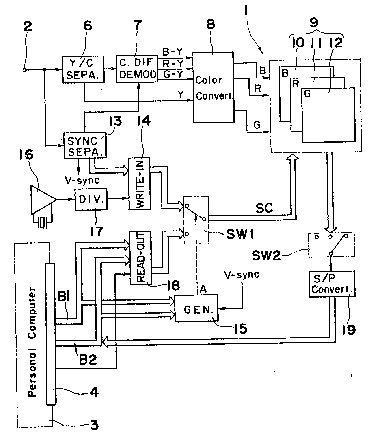
Referring first to Fig. 1, there is -
illu~trated a circuit block diagram of a still picture
read/write system 1. The system 1 shown therein
includes an input terminal 2 adapted for being connected
with a video output device, for example, a television
receiver set or a video tape player, and for being
connected a composite video signal that is applied from
the video output device. A connector 4 is adapted to be
connected with an address bus and a data bus of a
personal computer 3.
The composite video signal inputted to the
input terminal 2 is fed to a luminance signal separator
6 operable to separate signals from a luminance ~ignal Y
which is in turn applied to a color difference signal
-8- 1332~1
demodulator 7 for producing B-Y, R-Y and G-Y color
difference signals. The luminance signal Y from the
luminance signal separator 6 and the three color
difference signals from the color difference signal
S demodulator 7 are subsequently fed to a color
difference/primary color converter 8 operable to convert
the color difference signals into three primary color
signals, that is, B, R and G signals, which are
representative of the three primary colors, blue, red
and green. The primary color signals are in turn
supplied to a field memory device 9 in which the primary
color signals are digitized for storing therein in the
form of a still picture corresponding to one field.
The field memory device 9 includes three field
memories 10, 11 and 12 for the respective B, R and G
signals. Each of the field memories 10 to 12 employ a
serial access input and output system. Each of the
field memories 10 to 12 is of a memory construction
having 320 rows by 700 columns, a memory area having a
sufficient size to accommodate one picture, a one-line
buffer memory area and a row address counter. When each
of these field memories 10 to 12 applied with a serial
clock signal as will be described later are
incrementally shifted by a memory cell in a parallel
direction to the columns and, are applied with an
increment pulse signal, one line is shifted in a
parallel direction to the row. For the purpose of the
description of the preferred embodiment of the present
invention, each memory cell of each of the field
memories 10 to 12 is assumed to be capable of storing
one bit.
The composite video signal applied to the
input terminal 2 is also supplied to a sync separator 13
operable for separating horizontal and vertical
synchronizing signals from the composite video signal.
1~32~61
.: ,,
The outputs from the sync separator 13 is supplied to
the color difference signal demodulator 7 for clamping
and also to a WRITE-IN control circuit 14. The vertical
synchronizing signal separated from the composite video
signal by the sync separator 13 is also applied to a
control signal generator 15 as will be described later.
The WRITE-IN control circuit 14 is adapted to
receive a clock signal through a divider 17 which has
been generated from a WRITE-IN clock signal oscillator
16 having an oscillating frequency of, for example,
18.636 MHz. The WRITE-IN control circuit 14 is operable
to synthesize a plurality of WRITE-IN control signals on
the basis of the synchronizing signals, outputted from
the sync separator 13 and the clock signal generated
from the clock signal oscillator 16. These WRITE-IN
control signals are supplied to the field memory device
9 through a READ-OUT/WRITE-IN mode selector switch SWl.
The B, R and G signals outputted from the color
converter 8 are digitized and written in the field
memory 9 on the basis of the WRITE-IN control signals.
The details of the WRITE-IN operation will be described
later.
B. Still Picture Data Reading
The system 1 has an address bus Bl and a ~ata
bus B2 adapted for being connected with the address bus
and the data bus of the personal computer 3 through the
connector 4. Output signals from the personal computer
3 are supplied through the respective buses Bl and B2 to
a READ-OUT control circuit 18 and also to the control
signal generator 15. The READ-OUT control circuit 18 is
' f also adapted to receive a clock signal from the personal
computer 3 via the connector 4 having a frequency of,
for example, 4 MHz which is used within the domain of
the personal computer 3. The READ-OUT control circuit
18 is operable to synthesize a plurality of READ-OUT
1332461
- 10-
control signals on the basis of the outputs from the
personal computer 3 and the clock signal. These READ-
OUT control signals are supplied to the field memory
device 9 through a READ-OUT/WRITE-IN mode selector
S switch SW1.
When these READ-OUT control signals are
supplied to the field memory device 9, B, R and G color
data stored in the respective field memories 10 to 12
associated respectively with the B, R and G signals are
sequentially outputted to a primary color signal
selector switch SW2. The primary color signal selector
switch SW2 is controlled by a switching control signal
supplied from the personal computer 3 to sequentially
output blue color data, red color data and green color
data to a serial/parallel converter 19 in a specific
order, for example, in the order specified above.
The serial/parallel converter 19 is operable
to convert each of the color data into respective
parallel data which is in turn outputted to the personal
computer 3 through the data bus B2 for storage in a
graphic memory (not shown) built in the personal
computer 3. After the image signal is stored in the
graphic memory in the manner described hereinabove, the ~
image can be processed by operating the personal ~-
computer 3 in the usual manner well known to those
skilled in the art.
Fig. 2 illustrates a timing chart used to
explain the operation of the field memory device 9.
Fig. 2(1) illustrates a waveform of a portion of the
composite video signal corresponding to one horizontal
scanning period lH. A time span between timing t0 and
timing tl represents a horizontal blanking period, and a
time span T1 between timing tl and timing t2 represents
a duration of a video signal carrying picture ;
information. (See, Fig. 2(2)). In the illustrated
".: ' , . ' . . : . . ~: - !' "
-11- 133~61
instance, a serial clock signal SC shown in Fig. 2 (3),
is applied to the field memory device 9 to which the
composite video signal of the waveform described above
is supplied. Therefore, during a WRITE-IN period Tw
within the duration T1 of the video signal, the analog
video signal is digitized and written in the field
memory device 9 in the form of serial data.
Hereinafter, the READ-OUT operation of the
field memory device 9 will be described. The B, R and G
color data written, i.e., stored, in the field memory
device 9 are supplied to the personal computer 3 through
the data bus B2. The B, R and G color data written in
the respective field memories 10 to 12 associated
respectively with the B, R and G signals are
sequentially switched by the selector switch SW2 in the
order of blue color data followed by red color data
followed by green color data and are in turn outputted
to the data bus of the personal computer 3 after having
been converted by the serial/parallel converter 19 into
parallel color data. More specifically, when the data
written in the field memory device 9 are to be read out,
the converter 19 converts the data, serially supplied
from the field memory 10 for the B signal, from the very
beginning of such serially transmitted data into 8-bit
parallel data which are then outputted to the personal
computer 3. When all the blue color data written in the
field memory 10 have been read out in this manner, 8-bit
data are read out from the very beginning of the field
memory 11 for the R signal. Similarly, 8-bit data are
read out from the very beginning of the field memory 12
! 1 for the G signal. After all of the color data stored in
the field memory device 9 have been completely read out
in this way, the reading of one still picture is
completed. (See Fig. 3). It is eventually pointed out
that the reason for the employment of such a reading
,.
-12- 1~32461
method is because the data bus in the personal computer
3 has only an 8-bit capacity.
Fig. 4 illustrates a timing chart used to
explain the principle of operation of the system in the
illustrated instance. Referring to Fig. 4 in
combinatio~ with Figs. 1 to 3, the operation of the
selector switch SWl will now be described.
The selection between the READ-OUT mode and
the WRITE-IN mode of the image signal processor 1 is
accomplished by the selector switch SWl. More
specifically, when the selector switch SWl is in a
position for setting the processor in the WRITE-IN mode,
the WRITE-IN control signals outputted from the WRITE-IN
control circuit 14 are supplied to the field memory
device 9. On the other hand, when the selector switch
SW1 is moved to set the processor in the READ-OUT mode
(on the side of the personal computer 3), the READ-OUT
signals outputted from the READ-OUT control circuit 18
are supplied to the field memory device 9.
When the selector switch SW1 is in a position
for setting the processor in the READ-OUT mode, the
READ-OUT control circuit 18 supplies six types of READ-
OUT control signals including, for example, a READ-
OUT/WRITE-IN operation control signal RA5, the
previously mentioned serial clock signal SC, a refresh
control signal REF, an enable signal WE, an increment
signal INC and a row reset signal RCR, as shown by
signals (1) to ~6) in Fig. 5, respectively, to the field
memory device 9 through the selector switch SWl so that
the data stored in the field memory device 9 can be read
out therefrom.
By way of example, during a period between ;-
time Ts and time tn shown in Fig. 5, the red color data
for each still picture are read out from the field
memory 11 for the R signal. During a period between
-13- 1~32~61
time ta and time tb, the red data for one row are
serially read out in response to the serial clock signal
SC and the refresh control signal REF.
The switching operation of the selector switch
SWl is controlled by a switching control signal A
outputted from the control signal generator 15. More
specifically, when the switching control signal A is in
a low level state, the WRITE-IN mode is established, but
when the signal A is in a high level state, the READ-OUT
mode is established. (See the waveform (3) shown in
Fig. 4).
The control signal generator 15 includes, for
example, a D-type flip-flop and is operable to output
not only the control signal A, but also a clock
switching signal used to control the division cycle of ~;
the divider 17. As hereinbefore described, the vertical
synchronizing signal V outputted from the sync separator
13 is applied to the control signal generator 15. (See
the waveform (2) shown in Fig. 4).
Assuming that the processor 1 is set in the
WRITE-IN mode, and in the event that a command necessary
to ~et the processor 1 in the READ-OUT mode is generated
from the personal computer 3, a high level control
signal D iB supplied from the personal computer 3 to the
control signal generator 15. By way of example, when
the control signal D is rendered to be in a high level
state at a time t0 as shown by the waveform (1) in Fig.
4, the switching control signal A is set to a high level
state in response to the set-up of one of the vertical
synchronizing pulses V, which has been applied
immediately after the set-up of the control signal D to
the high level state, and the high level state of the
switching control signal A is subsequently maintained.
As the switching control signal A is set to
the high level state, the selector switch SW1 is brought
.,
, ~ ,, ,;, , " ~ ~
-- -14- 1332461
in position to set the processor l in the READ-OUT mode,
thereby permitting the data in the field memories lO to
12 to be read out sequentially. More specifically,
during a period from a time t2 to a time t3 shown in
Fig. 4, the blue color data are first supplied to the
personal computer 3. During a subsequent period from
the time t3 to a time t4, and during a period from the
time t4 to a time t5, the red color data and the green
color data are successively and sequentially supplied to
the personal computer 3, respectively. In this way, at
the time t5, the still picture data for one still
picture which have been written in the field memory
device 9 are completely read out from the field memory
device 9 and transferred to the personal computer 3.
As hereinafter described, the switching
between the WRITE-IN and READ-OUT modes can be
accomplished when the control signal D transmitted from
the personal computer 3 is brought in a high level
state. The effective timing of this switching is
synchronized with the set-up of one of the vertical
synchronizing pulses which is applied immediately after
the control signal D has been brought in the high level
state. Specifically, the switching into the READ-OUT
mode is carried out during a vertical blanking period TB
as shown in the waveform (7) in Fig. 4.
Upon the completion of the read-out of the
image signal, the personal computer 3 causes the control
signal D to be in a low level at a time t6 wherefore the
switching control signal A, which is an output from the
control signal generator 15, is in a low level state in
response to the set-up of another one of the vertical
synchronizing pulses V which is applied immediately
thereafter, i.e., at a time t7 shown in Fig. 7, and
causes the selector switch SWl to set the processor l in
the WRITE-IN mode. It is to be noted that the time t7
-1S- 1332461
is immediately after the color data in the field memory
device 9 have been read out from the field memory device
9, and no data is written in the field memory device 9.
Accordingly, after the time t7, the image signal
S subsequently inputted can be written again in the field
memory device 9 in the form of a still picture.
The reason for switching the READ-OUT mode
during the vertical blanking period TB is for the
purpose of accurately reading out the video signal
corresponding to one picture. If this switching is not
effected during the vertical blanking period TB, the
picture being reproduced on a screen may be switched
over to a different picture without being completely
reproduced. The time required to complete the read-out
of one picture is determined by the timing at which the
control signal D from the personal computer 3 is brought
in the high level state. More specifically, since the
start and end of the period during which the information
read-out is carried out lie within the time span between
the neighboring vertical blanking periods, a wait time
occurs before and after the read-out operation. In any
event, in the illustrated instance, the time required to
complete the information read-out may be 0.2 second on
an average.
The time required to complete the write-in
operation which takes place when the processor 1 is set
in the WRITE-IN mode corresponds to one field period,
that is, 1/60 second. As hereinbefore described, upon
the completion of the read-out operation, the processor
1 is switched into the WRITE-IN mode to permit the color
` data corresponding to one still picture to be again
written in the field memory device 9.
Also, the timing at which the processor 1 is
switched onto the WRITE-IN mode is carried out during
the vertical blanking period. Accordingly, the personal
~".
~ ;i ~
-16- 1332461 :~
,:,
computer 3 can render the control signal D to be in a
high level state for any timing. More specifically,
regardless of when the personal computer 3 generates a
command required to bring the control signal D into the
high level state, the color data corresponding to one
still picture can be always read out accurately.
Moreover, the switching of the image signal processor 1
into the READ-OUT mode can be reliably accomplished
without interrogations being carried out such as in the
prior art processor. Accordingly, the still picture
represented by the video signal can be written at a high
speed in the graphic memory device built in the personal
computer.
As hereinbefore described, in the image signal
processor according to the present invention, when the
memory is desired to be brought in the READ-OUT READY
condition, this condition can be accomplished merely by
causing the operating device to output the READ-OUT
command. Accordingly, the necessity of frequent
interrogations between the processor and the operating
device that are required in the prior art processor can
be minimized, and the read-out operation of the memory
can be carried out at a high speed. Moreover, since the
timing at which the switching between the WRITE-IN and
READ-OUT modes takes place in synchronism with the
vertical synchronizing signal and without relying on the
timing at which the READ-OUT command is transmitted, the
video signal corresponding to one field period can be
always read out accurately.
C. Still Picture Data Writing:
A first embodiment of an image signal
processing according to the present invention will now
be described.
Referring to Fig. 6, a waveform (a) shown
therein represents that of the image signal carrying a
, ,
-17- 1 332~6~
still picture, wherein a chain line A represents an
average level of the image signal. Those portions of
the image signal which are located around the average
level denoted by the chain line A are superimposed with
S clock pulses whose waveforms are shown by (c) in Fig. 6.
When the image signal superimposed with the clock pulses
ic inputted to a switching element having a threshold
value equal to the average level, a digitized signal of
a waveform as shown by signal (d) in Fig. 6 can be
obtained.
For the purpose of comparison, a digitized
signal obtained by inputting the image signal, which is
not superimposed with the clock pulses, to the same
switching element is shown by signal (b) in Fig. 6. As
can be understood from Fig. 6, a portion of the image
signal which is of a level higher than the average level
represents a bright region while a portion of the image
signal which is of a level lower than the average level
represents a dark region. ~n the other hand, according
to the waveform (d), a portion in which the bright and
dark regions alternates finely, that is, a region of
intermediate gradations shows up between the bright and
dark regions. By way of example, where the still
picture image is presented in black and white, the
region of intermediate gradations is shown in gray.
Also, where the input image signal is a red color
signal, the region of intermediate gradations is
represented by a repetition of red and black colors and
is, therefore, represented by a brown color which is an
intermediate color between the red color and the black
color. The region of intermediate gradation is
attributable to the clock pulses superimposed on the
image signal in the manner as hereinabove described.
In view of the foregoing, if the digitized
signal of the waveform (d) shown in Fig. 6 is sampled at
-18- ~ 332~61
a timing shorter than the cycle of the clock pulses and
is then stored in, for example, a sufficient memory
device having a memory capacity to accommodate one still
picture, the digitized signal for the intermediate
S gradations can be read out at any desired time.
Fig. 7 illustrates another embodiment of the
method for the present invention. According to the
embodiment shown in Fig. 7, the image signal having
portions superimposed with the clock pulses at the
average level is divided into eight levels 0 to 7 so
that it can be converted into a 3-bit digital signal as
shown by waveform (a) in Fig. 7. A waveform (b) shown
in Fig. 7 represents the 3-bit digital signal converted
from the analog signal. A waveform (c) shown in Fig. 7
represents the 3-bit digital signal which has been
further converted into an analog signal. In contrast
thereto, waveforms associated with the image signal not
superimposed with the clock pulses, which have been
converted into the digital signal, are illustrated in
Fig. 8.
As can be readily understood from the
comparison between the waveforms (c) shown in Figs. 7
and 8, a component resulting from the image signal
superimposed with the clock pulses fills up steps
between gradations of the image signal so that the
intermediate gradations or the intermediate colors can
be displayed. Because of this, when the still picture
i8 to be reproduced, the superimposition with the clock
pul6es achieves an effective result reproducing the
still picture in a color as faithful as possible to the
color of the original image. In other words, at
portions where the clock pulses are superimposed, a
resolving power can be equivalently increased. In order
to in¢rease the resolving power, the number of bits of
the analog-to-digital converter is generally required to
1332461
-19-
be increased. The present invention is effectlve for
accomplishing a substantially faithful color
reproduction, including the reproduction of intermediate
gradations and intermediate colors, without requiring
S the number of bits of the analog-to-digital converter to
be increased.
The image signal processor necessary to
achieve the above described objective will now be
described with particular reference to Figs. 9 and 10.
Fig. 9 illustrates a second embodiment of the
image signal processor according to the present
invention and Fig. 10 illustrates an intermediate
gradation generator used in the circuit shown in Fig. 9.
The luminance signal as a video signal
indicative of a still image is applied to an
intermediate gradation generator 20. The intermediate
gradation generator 20 includes, as best shown in Fig.
10, an NPN-type switching transistor TRl having a
threshold level substantially equal to the average level
of the luminance signal of the still image. The
traneistor TRl has a base to which a resistor R1 and a
speed-up capacitor Cl are connected. A set-up improving
diode D1 i5 connected between the base and the collector
of the transistor TR1 in a forward direction. The base
of the transistor TR1 is grounded through a resistor R2.
The transistor TR1 has its collector connected with a
direct current source line +B through a resistor R3 and
its emitter connected to the ground. The base of the
transistor TRl is also connected with a clock pulse
generator 23 through a series circuit having a DC
element capacitor C2 and a resistor R4. The clock pulse
generator 23 is of a type capable of generating clock
pulses of 3 MHz in frequency and is adapted to receive a
vertical drive signal operable to lock the oscillation
of the clock pulse generator 23.
.' ' , . ::: ' . ' ~ ,.:,.` ` . ., ' ' , `
~ -20- 133246~
An output from the intermediate gradation
generator 20 of the construction described with
particular reference to Fig. 10 is supplied to a memory
unit 21 which is controlled by a control unit 22.
S Contents stored in the memory unit 21 are read out to
the color difference/primary color converter 8 from
which the image data is outputted to an external display
device.
The image signal processor according to the
lo second embodiment of the present invention shown in and
described with reference to Figs. 9 and 10 will now be
described.
Let it be assumed that the luminance signal of
the still image having the waveform shown by signal (a)
in Fig. 6 is applied to the base of the switching
transistor TR1.
The 3 MHz clock pulses generated from the
clock pulse generator 23 are also applied to the base of
the transistor TRl through the resistor R4 and the
capacitor C2. Since the direct current component of the
clock pulses are inhibited by the action of the
capacitor C2, the level of the clock pulses to be
superimposed on the luminance signal varies with the
level of the luminance signal. In other words, the ;
amplitude of the clock pulses superimposed on the
luminance signal is high for the average level of the
luminance signal, but low for a lower or a higher level
of the luminance signal as can be understood from the
waveform (c) shown in Fig. 6~
Since the transistor TR1 has a threshold level
substantially egual to the average level of the
luminance signal, a digitized signal of the luminance -
signal, which is an output from the transistor TR1, will
represent such a waveform having an intermediate
portion, as shown by (d) in Fig. 6.
-21- 1332~61
This digitized signal is then supplied to the
memory unit 2l. The memory unit 2l is controlled by the
control unit 22 to sample out the digitized signal at a
timing (28.636 MHz in this instance) shorter than the
cycle of the clock pulses superimposed on the luminance
signal for storing the luminance signal corresponding to
one still picture. The contents stored in the memory
unit 21 are, in response to a control signal applied
from the control unit 22, supplied to the external
display device, for example, the personal computer 3,
after having been converted into parallel signals as
hereinbefore described. The still picture having
intermediate gradations is then displayed through a
cathode ray tube of the personal computer 3. At this
time, as hereinbefore described, the clock pulses
superimposed on the luminance signal are synchronized
with the vertical drive signal. Therefore, even though
a difference beat component may occur as a result of the
difference between the luminance signal and the clock
pulses, the beat component is held still when viewed in
terms of the vertical synchronization. Accordingly, a
phenomenon in which any possible fringe resulting from
the beat component will not move on the screen of the
cathode ray tube, which is not comfortable to look, can
be substantially eliminated.
In describing the second embodiment of the
present invention, the luminance signal has been
described as a digitized signal. However, the present
invention is not limited thereto, but may be applicable
where each of the R, G and B signals is digitized.
The image signal processor according to a
third embodiment of the present invention is illustrated
in Figs. ll to 13. Specifically, Fig. ll illustrates a
circuit block diagram of the image signal processor
according to the third embodiment, Fig. 12 illustrates
-~ -22- 1332~61 :~
the details of an intermediate gradation generator used
in the image siqnal processor of Fig. 11 and Fig. 13
illustrates respective waveforms of various signals
appearing in the circuit of Fig. 12.
S Referring first to Fig. 11, the primary color
signals, that is, the R, G and B color signals, emerging
from the color difference/primary color converter 8 are ~-~
supplied to an intermediate gradation generator 70 which
provides R', G' and B' signal corresponding respectively
to the R, G and B color signals having average level
portions superimposed with the block pulses. ;~
As best shown in Fig. 12, the intermediate
gradation generator 70 includes three direct current
amplifiers 71, 72 and 73 of identical construction.
lS Each DC amplifier 71 to 73 includes a PNP-type
transistor TR2 having a base to which the associated
primary color signal is applied from the converter 8.
The transistor TR2 also has an emitter connected to a
power source line +B through a resistor R5 and a
capacitor C3 connected in parallel to each other. The
collector of the transistor TR2 is grounded through a
resistor R6 and is connected to the base of an NPN-type
transistor TR3 having its collector connected to the
power source line +B through a resistor R7. The emitter
of the transistor TR3 is grounded through a resistor R8.
The transistor TR3 has its base connected through a
direct current inhibiting capacitor C4 and a resistor R9
to a clock pulse generator 74 to which the vertical
drive signal is supplied. The clock pulse generator 74
is adapted to generate clock pulses of 3MHz in frequency
and synchronized with the vertical drive signal. A node
between an output terminal of the clock pulse generator
74 and the capacitor C4 is grounded through a variable
resistor VR4.
~ -23- ~332461
Referring back to Fig. 11, the R ', G ' and B'
signals outputted from the intermediate gradation
generator 70 are supplied respectively to analog-to-
digital converters 81, 82 and 83. In each analog-to-
S digital converter, one analog data for one picture
element is converted into 3-bit data. The digital data
produced respectively from analog-to-digital converters
81, 82 and 83 are applied and stored in associated
memories 91, 92 and 93, respectively. When compared
with memory 10 shown in Fig. 1 for the blue data in the
embodiment of Fig. 1, the memory 93 shown in Fig. 11 for
the blue data substantially has a three times greater
capacity. The same can be said for the other two
memories 91 and 92. Respective outputs from the
memories 91, 92 and 93 are supplied to associated
digital-to-analog converters 101, 102 and 103 which
provide respective outputs to the external display
device, for example, a monitor television receiver.
It is to be noted that the converters 81 to
83, the memories 91 to 93 and the converters 101 to 103
are all controlled by the control unit 14 to which
horizontal and vertical synchronizing pulses are
supplied from the sync separator 13.
The operation of the image signal processor
according to the third embodiment of the present
invention shown in and described with reference to Figs.
11 and 12 will now be described with reference to Fig.
13.
As hereinbefore described, the R, G and B
color signals, emerging from the color
difference/primary color converter 8 are supplied to an
intermediate gradation generator 70 which in turn ;
provides R', G' and B' signal corresponding respectively
to the R, G and B color signals having average level
portions superimposed with the clock pulses. In Fig.
-24- 1 ~ 32461 :
13, the waveform of only one of the R, G and B signals,
for example, that of the R signal which is applied to
the DC amplifier 71, is shown by S1 for the purpose of
this discussion.
On the other hand, when the vertical drive
signal identified by S5 and having such a waveform as
shown by signal (e) in Fig. 13 is supplied to the clock
pulse generator 74, the latter generates the clock
pulses S4 having a waveform as shown by signal (d) in
Fig. 13. The clock pulses S4 are, after DC components
thereof have been cut out by the action of the capacitor
C4, inputted to the base of the transistor TR3.
Accordingly, the signal S2 applied to the base of the
transistor TR3 has a waveform as shown by signal (b) in
Fig. 13, which signal S2 is then inverted by the s
transistor TR3 to provide the associated R', G' or B'
signals S3 which correspond to the inputted color signal
having average level portions superimposed with the
clock pulses as shown by a waveform (c) in Fig. 13.
It is to be noted that, if the amplitude of
the clock pulses is too high, it may happen that the
black level will be highlighted or the white level will
be faded out with the consequence that the still picture
reproduced on the monitor television screen will be
grayish. In order to substantially eliminate this
problem, it is preferred that the resistance setting of
the variable resistor VR be selected as to permit the
clock pulses to be superimposed on those portions of the
input color signal which are of the average level.
The respective R', G' and B' color signals
with the clock pulses superimposed thereon are thén
supplied to the associated analog-to-digital converters
81 to 83 by which they are converted into the 3-bit
digital signals. At this time, the sampling frequency
is controlled by the control unit 14 to be higher than
.
~3~
the frequency (3 MHz) of the clock pulses superimposed
on the respective color signals. In the illustrated
instance, the sampling frequency employed is 3B.636 MHz.
The 3-bit digital signals outputted from the
S respective converters 81 to 83 are then supplied to theassociated memories 91 to 93, and the three bits of each
of the digital signals are stored in memory areas 91a,
91b and 91c of the respective memories 91, 92 or 93.
The color signals so stored are read out from
the associated memories 91 to 93 in response to the
control signal fed from the control unit 14, and
converted by the converters 101 to 103 into respective
analog signalP which are in turn outputted to the
monitor television receiver (not shown).
As hereinbefore described, the image signal
processing method according to the present invention is
such that the clock pulses are superimposed on the
portions of the image signal which are of a value
substantially equal to the average level and are then
sampled out at a timing smaller than the cycle of the
clock pulses to provide the image signal to the external ;
display device. Accordingly, any intermediate gradation
or color of the original image can be faithfully
reproduced.
Moreover, the image signal processor according
to the second embodiment of the present invention ~;
includes the switching transistors operable to
superimpose the clock pulses on the portions of the
image signal which are of a value substantially equal to
the average level and then to digitize the image signal.
The threshold values of the switching transistors need
not be varied as required in the conventional Dither ~
method. Therefore, faithful reproduction of the ~ ;
intermediate gradations or colors can be accomplished
reliably.
! ! ' ~ C
~ -26- ~33246~
Furthermore, the present invention does not
require any process hitherto needed to combine a
plurality of digitized images. Therefore, the image
signal indicative of the still picture can be outputted
on a real-time basis.
The image signal processor according to the
third embodiment of the present invention is designed so
that the portions of the image signal indicative of the
still picture which are of a value substantially equal
to the average level of the image signal are
superimposed with the clock pulses and are then
amplified by direct current. The amplified signal is
subsequently sampled out at a timing smaller than the
cycle of the clock pulses and then converted into the
digital signal for storage in the memory. According to
this embodiment of the present invention, since the
resolving power of that portion where the clock pulses
are superimposed is substantially increased and,
therefore, the number of bits of the converters and the
memories need not be increased in order to increase the
resolving power. Thus, the use of the memory unit of a
minimized memory capacity is sufficient for the
intermediate gradations and intermediate colors inherent
in the original image to be faithfully reproduced.
C-a. Still Picture Data Writing (Modification 1):
Referring to Figs. 14 and 15 which illustrate
the circuit block diagram for a modified form of the
image signal processor and respective waveforms of
various signals appearing in the circuit of Fig. 14, the
image signal processor shown therein basically includes
, a converter unit 1 operable to modulate the composite
color video signal into the color difference signals.
Also, those color difference signals and the composite
color video signal are operable to modulate or matrix
for providing primary color signals on which components
-27- 13324~1
of a carrier color signal of 3.58 MHz are superimposed;
first to third analog-to-digital converter 81, 82 and 83
which word as digitizing circuits for digitizing the
outputs from the converter unit 1 at a predetermined
S threshold level; a clock pulse generating unit 30 for
providing clock pulses synchronized with a color burst
signal, included in the composite color video signal and
having a frequency n-times (n being a positive integer
not smaller than 2) the frequency of the color burst
signal; and first to third memories 10, 11 and 12
adapted to receive the clock pulses form the clock pulse
generating unit 30 as sampling clock pulses for sampling
and storing respective outputs from the first to third
converters 81 to 83.
The converter unit 1 includes a Y/C separator
6 for separating the color signals from the composite
color video signal applied to the input terminal 2; a
color difference signal demodulator 7 for demodulating
from the color signals, fed from the Y/C separator 6,
color difference signals B-Y, R-Y and G-Y of respective
waveforms shown by signals (c), (d) and (c) in Fig. 15; ~;~
a fourth transistor TRd for inverting and amplifying the
composite color video signal to such a waveform as shown
by signal (b) in Fig. 15; and a converter 8 having first
to third transistors TRa, TRb and TRC which are operable -
to modulate or matrix the color difference signals B-Y, -
R-Y and G-Y, fed from the demodulator 7, and the
composite color video signal which has been inverted by
the transistor TRd. Thereby respective negative primary
color signals B, R and G are provided which have been
superimposed with the components of the carrier color
signal of 3.58 MHz.
The first to third transistors TRa to TRc
forming the color difference/primary color converter 8
-28- 133~461
have their bases, to which the color difference signals
B-Y, R-Y and G-Y are applied, respectively, and their
emitters to which the inverted composite color video
signal is applied. These transistors Tra to TRc output
S the respective primary color signals B, R and G which
have been superimposed with the carrier color signal
components.
Unlike the embodiments shown and described
with reference to Figs. 6 to 13 and what has been
lo disclosed in Japanese patent Publication JPA 62-24174
published November 5, 1987, in the image signal
processor according to the modification now under
discussion, the carrier color signal of 3.58 MHz
included in the composite color video signal is used as
lS the clock pulses, without the image signal being
superimposed with the clock pulses, while use has been
made of the converter 8 for providing the primary color
signal on which the carrier color signal components have
been superimposed.
With the above described construction, a
structure to superimpose the clock pulse is not required
and, therefore, the image signal processor can be
advantageously simplified. Moreover, since the
composite color video signal can be applied directly to
the emitters of the transistors TRa to TRc without being
passed through the Y/C separator, the frequency
characteristic of the luminance signal can be improved,
as compared with the case in which the Y/C separation is
carried out, thereby accomplishing a high quality
picture reproduction.
The luminance signal emerging from the Y/C
separator 6 is supplied to the sync separator 13 by
which synchronizing signals are separated from the
luminance signal. The synchronizing signals are then
-29- 1332461
applied to a control unit (not shown) so that the A/D
converters 81 to 83, the memories 10 to 12 and the D/A
converter 101 to 103 can be controlled by the control
unit.
The first to third A/D converters 81 to 83
work to convert the primary color signals B, R and G,
which have been superimposed with the carried color
signal components, into respective digitized signals in
a manner which will now be described.
Figs. 16 and 17 illustrate waveforms used to
explain how each of the primary color signals is
digitized, for example, the blue color signal, with the
carrier color s,ignal component superimposed thereon by
the analog-to-digital converter 81. When the blue color
signal with the carrier color signal component
superimposed thereon, having such a waveform as shown by
signal (A) in Fig. 16, is supplied to the associated A/D ;
converter 81 having a predetermined threshold level as
indicated in Fig. 3, the converter 81 operates to invert
the input signal of a higher level than the threshold
level into a low level signal and also to invert the
input signal of a lower level than the threshold level
into a high level signal. Accordingly, when an input ;~
signal as shown by the waveform (A) in Fig. 16 is
inputted to the associated converter 81, the latter
outputs the digitized signal of a waveform shown by
signal (B) in Fig. 16.
Fig. 17 illustrates, on an enlarged scale, a
portion of the waveform (A3 of Fig. 16 in the vicinity
of the threshold level and also a portion of the
waveform (B) of Fig. 16 corresponding to that portion of
the waveform (A) shown in Fig. 17. as can be readily
understood from the waveforms (A) and (B) shown in Fig. -
17, if the higher level portion of the blue color signal
,: :
30- 13 3 2 46
represents a yellow color and the lower level portion of
the same blue color signal represents a cyan color, the
yellow and cyan colors alternate during a period in
which the level of the blue color signal changes from
S the higher level down to the lower level relative to the
predetermined threshold level, thereby representing an
intermediate color between the yellow and cyan colors.
In this example, since the pulse width (duty ratio) of
the carrier color signal component, which is used as the
clock pulses, during one cycle thereof progressively
varies (varies in a direction in which the pulse width
is reduced, in the case of the waveform (B) shown in
Fig. 4), with respect to the threshold level, the
intermediate gradation correspondingly varies.
In this way, based on the primary color signal
with the carrier color signal component superimposed
thereon, a so-called quasi-intermediate color can be
formed.
On the other hand, the clock pulse generating
unit 30 includes a fifth transistor TRe operable to
shape the color burst signal supplied from the
demodulator 7, and a PLL circuit for generating clock
pulses synchronized with the shaped color burst signal
and having a frequency four times the frequency of the
color burst signal, that is, 14.32 MHz (=3.58 x 4).
This PLL circuit includes a voltage controlled
06cillator (VCO) 36 capable of generating clock pulses
having a frequency which is four times the frequency of
the color burst signal, a divider 34 for dividing the
frequency of the output from the oscillator 36 by 4, and
a phase comparator 32 for comparing the phase of the
output from the divider 34 with that of the color burst
signal and for applying an error voltage to the voltage
controlled oscillator 36 which corresponds to the phase
-31- 1332~61
difference between the output from the divider 34 and
the color burst signal.
Each of the memories 10 to 12 is operable to
sample out and store the digitized signal from the
S associated A/D converter with the clock pulses from the
generating unit 30 used as sampling clock pulses.
The digitized signals read out from the ;
respective memories 10 to 12 are, after having been
converted into the analog signals by the associated
digital-to-analog converters 101 to 103, supplied to the
external display device (not shown) such as, for
example, a monitor television receiver or the personal
computer 3.
The sampling clock pulses supplied to each of
the memories 10 to 12 are synchronized with the color
burst signal and, hence, the carrier color signal
components of 3.58 MHz used as the clock pulses
superimposed on the primary color signal outputted from
the converter unit 1. Therefore, interference fringes
resulting from a beat component occurring as a result of
the difference between the image signal and the carrier
color signal components are stabilized and, therefore,
the still picture is reproduced having more viewing
comfort. Moreover, since the frequency of the sampling
clock pulses is made to be an integer multiple of the
frequency of the carrier color sisnal components, that
is, the frequency of the color burst signal, the
interference fringes are completely regular and lined up
in a longitudinal of the television screen. Thereby,
the still picture that is reproduced thereon has a
greater viewing comfort.
According to the modified form of the image
signal processor described above, since the primary
color signals whicih have been superimposed with the
carrier color signal components are digitized at ~-
~- -32- 133~
. . ,
respective portions in the vicinity of the threshold
levels, the number of bits of the converters and the
memories need not be increased in order to increase the
resolving power. Thus, the use of the memory unit of a
minimized memory capacity i8 sufficient for the
intermediate gradations and colors inherent in the
original image to be faithfully reproduced.
Moreover, when the primary color signals
having the carrier color signal components superimposed
thereon are to be formed, the composite color video
signal can be applied directly without being passed
through the Y/C separator, the quality of the still
picture reproduced can be improved, as compared with the
case in which the Y/C separation is carried out.
C-b. Still Picture Data Writing (Modification 2):
Referring to Figs. 18 and 19 which illustrate
the circuit block diagram of another modified form of
the image signal processor and respective waveforms of
various signals appearing in the circuit of Fig. 18, the
image signal processor shown therein includes a clock
pulse generator 40 having a control unit 42 for
generating second clock pulses of 14.318 MHz in
frequency which are used as the sampling clock pulses to
be applied to the memories 10 to 12 and also for
generating clock pulses to be applied to the A/D
converters 81 to 83 in a manner as will be described
later, and a 1/4 divider 44 for dividing the frequency
(14.318 MHz) of the second clock pulses by 4 to provide
first clock pulses having a frequency of 3.58 MHz. The
waveform of the first clock pulses is shown by signal
(c) in Fig. 19. Therefore, the second clock pulses are
synchronized with the first clock pulses and have a
frequency n (n being a positive integer not smaller than
2, for example, n is 4 in this illustrated instance)
times the frequency of the first clock pulses.
r;
'~" ' '~ ' ' ' , , ~ ' ' '
~; ~33~ 1332461
Reference numeral 46 represents a clock pulse
superimposing circuit 5 for superimposing the first
clock pulses, supplied from the divider 44 of the clock
pulse generating unit 40, on the luminance signal Y for
S providing a superimposed luminance signal. This
superimposing circuit 5 together with the color
difference/primary color converter 8, which operates to
add the color difference signals B-Y, R-Y and G-Y to the
superimposed luminance signal, and the A/D converters 81
to 83 are operable to provide the respective digitized
signals, form a quasi-intermediate color generating
device. The waveform of the superimposed luminance
signal generated from the superimposing circuit 46 is
illustrated by signal (d) in ~ig. 19 while the luminance
signal supplied to the superimposing circuit 46 is
illustrated by signal (b) in Fig. 19. Also, one of the
color difference signals, for example, the color
difference signal B-Y is shown by signal (a) in Fig. 19,
and one of the digitized signals, for example, the
digitized signal emerging from the A/D converter 81 is
shown by signal (e) in Fig. 19.
The clock pulse superimposing circuit 46
includes a transistor TRg having the first clock pulses
applied to its base, a variable resistor VRx for
adjusting the level of the first clock pulses outputted
from the transistor TRf, a DC inhibiting capacitor Cx
for cutting off a DC component of the first clock
pulses, and a transistor TRf having the luminance signal
Y applied to its base, the transistor TRf being operable
for superimposing the first clock pulses, applied to the
emitter thereof, on the luminance signal Y. The DC
inhibiting capacitor Cx improves the frequency
characteristics of the image signal. More specifically,
the DC inhibiting capacitor C constitutes an emitter-
peaking by the transistor TRf. Accordingly, if the
~. '".
34 1332~61
capacitance of the capacitor Cx is reduced, a highfrequency region of the image signal will be enhanced
for highlighting the color of intermediate gradations
where a considerable change in picture takes place.
S Thereby, the quality of the still picture being
reproduced is improved.
The color difference/primary color converter 8
includes the first, second and third transistors TRa,
TRb and TRc having the respective color difference
signals respectively applied to their bases. Also, the
superimposed luminance signal, that is, the luminance
signal having the first clock pulses superimposed
thereon, is applied to their emitters. These
transistors TRa to TRc output from their collectors
respective added signals in which the superimposed
luminance signal and the color difference signals are
summed together.
When the added signals from the converter 8
are inputted to the respective A/D converters B1 to 83,
the added signals are converted by the converters 81 to
83 into respective digitized signals of a waveform shown
by signal (e) in Fig. 19.
The memories 10 to 12 and the D/A converter~
101 to 103 respectively operate similar to the manner
described in connection with the previous modified form
of the image signal processor shown and described by
Fig. 14.
The image signal processor of the construction
described hereinabove with reference to Fig. 18 operates
in the following manner. For the purpose of
simplification, reference will be made only to the color
difference signal B-Y in describing the operation of the
image signal processor. However, it is noted that the
following description can be equally applicable to the
other color difference signals R-Y and G-Y.
1332461
The color difference signal B-Y outputted from
the demodulator 7 has a waveform shown by signal (a) in
Fig. 19 and is applied to the base of the transistor
TRa.
S On the other hand, the second clock pulses
from the control unit 42 are divided by the divider 44
to provide the first clock pulses of the waveform shown
by signal (c) in Fig. 19. The first clock pulses
emerging from the divider 44 are supplied to the emitter
of the transistor TRf through the base-emitter path of
the transistor TRg and then through the DC inhibiting
capacitor Cx. The transistor TRf has the luminance ;
signal of the waveform, shown by signal (b) in Fig. 19,
applied to its base. Therefore, the superimposed
luminance signal emerge is developed from the color of
the transistor TRf. The superimposed luminance signal
develops a waveform shown by signal (d) in Fig. 19.
This superimposed luminance signal outputted from the
transistor TRf is supplied to the emitter of the
transistor TRa of the color converter 8.
Since the color difference signal B-Y and the
superimposed luminance signal Y are summed together by ;
the transistor TRa, the transistor TRa outputs the blue
color signal B on which the clock pulses have been
superimposed from its collector. This blue color signal ;
B is then digitized by the associated A/D converter 81
into the digitized signal having the waveform (e) shown
in Fig. 19.
Fig. 20 illustrates waveforms used to explain
how the blue color signal having the clock pulses
! I ' superimposed thereon is digitized by the analog-to-
digital converter 81. When the blue color signal having
the clock pulses superimposed thereon as shown by the
waveform (a) in Fig. 20 is supplied to the A/D converter
81 having a predetermined threshold level as indicated
~~ -36-
in Fig. 20, the converter 81 operates to invert the
input signal of a higher level than the threshold level
into a low level signal. Also, the input signal of a
lower level than the threshold level is inverted into a
S high level signal. Accordingly, when the input signal
shown by the waveform (a) in Fig. 20 is inputted to the
converter 81, the digitized signal of the waveform (b~
shown in Fig. 20 is outputted from the converter.
Fig. 21 illustrates, on an enlarged scale, a
portion of the waveform (a) of Fig. 20 in the vicinity
of the threshold level and a portion of the waveform (b)
of Fig. 20 corresponding to that portion of the waveform
(a) shown in Fig. 21. As can be readily understood from
the waveforms (a) and (b) shown in Fig. 21, if the
lS higher level portion of the blue color signal represents
a yellow color and the lower level portion of the same
blue color signal represents a cyan color, the yellow
and cyan colors alternate during a period in which the
level of the blue color signal changes from the higher
level down to the lower level relative to the
predetermined threshold level. Thereby, an intermediate
color between the yellow and cyan colors is represented.
In this example, since the pulse width (duty ratio) of
the carrier color signal component, which is used as the
clock pulses, during one cycle thereof progressively
varies (varie~ in a direction which reduces the pulse
width, in the case of the waveform (b) shown in Fig. 21)
with respect to the threshold level, the intermediate
gradation correspondingly varies.
The second clock pulses emerging from the
control unit 42 are supplied not only to the divider 44,
but also to the memories 10 to 12 as the respective
sampling clock pulses. In response to the sample clock
pulses, the memories 10 to 12 store and process the
respective outputs from the A/D converters 81 to 83.
37 ~ 6~
The color signals stored in the associated memories 10
to 12 are, in response to the control signal from the
control unit 42, outputted to the associated D/A
converters 101 to 103 from which the analog signals are
outputted to the external display device for the
reproduction on a screen of the cathode ray tube.
In the modification shown and described by
Fig. 18, since the sampling clock pulses supplied to the
memories 10 to 12 and the first clock pulses to be
superimposed on the luminance signal are synchroniied
with each other, any possible interference fringe which - -
would appear on the television screen as a result of a
beat component between the luminance signal and the
~ clock pulses can be advantageously stabilized. In
addition, since the sampling clock pulses are selected
to have a frequency four times the frequency of the
first clock pulses, the interference fringes will be
lined up in a longitudinal direction of the screen,
permitting the reproduced still picture to be
comfortably viewed.
It is to be noted that the inversion of the
phases of the clock pulses for each horizontal scanning
line may render the interference fringes to be arranged
in a grid shape for permitting a more comfortable
viewing of the still picture reproduced.
Even the image signal processor shown and
described by Fig. 18 can bring about such advantages and
effects as hereinbefore described in connection with any
one of the foregoing embodiments.
Although the present invention has fully been
described in connection with the preferred embodiments
thereof with reference to the accompanying drawings, it
is to be noted that various changes and modifications
are apparent to those skilled in the art. Such changes
and modifications are to be understood as included
-38- ~3~
within the scope of the present invention unless they
depart therefrom.
, ~ .
.
I; ! ~ I , . . .
.
,~
~-J~