Note : Les descriptions sont présentées dans la langue officielle dans laquelle elles ont été soumises.
1 3341 58
IMPROVED METALLI~ATION FOP~ SEMICONDUCTOR DEVICES
Technical Field
This invention relates generally to the field of
semiconductor devices and particularly to such devices
S embodied in integrated circuits. Even more particularly,
this invention relates to integrated circuits having
encapsulated bimetallic metallizations and to a method for
producing the encapsulated bimetallic metallization.
BaCk~E____of_t_e_I__e_tiO_
Integrated circuits require metallizations to
connect the various individual devices within the
integrated circuit. As both the complexity and the number
of devices in the integrated circuits increase, the
dimensions of the lines forming the interconnections,
i.e., metallizations, generally decrease as does the
spacing between the lines. Although there are often
problems associated with the integrity of the lines, these
problems become still more severe in very large scale
integration (VLSI) due to the very small dimensions of the
lines.
Aluminum is frequently the preferred
metallization because of its relatively low resistivity
and its compatibility with doped silicon. There is the
potential for at least four problems to arise from the use
of the aluminum. First, aluminum is not a very hard metal
and it is possible to scratch the metal before it has been
passivated. Second, electromigration of atoms within the
lines is possible. Electromigration potentially leads to
electrical discontinuities in the line. This problem can
be alleviated, and perhaps solved, by depositing the
aluminum in a bamboo type structure which stops the
electromigration. See U. S, Patent 4,438,450 issued on
March 20, 1984. Third, for many applications, it is
- 2 - 1 334 1 58
desirable to deposit the metallization over
discontinuities or steps in the physical surface while
retaining electrical continuity. This is often difficult
to realize with conventional deposition techniques.
S Fourth, the aluminum lines may develop either or both
lateral or vertical hillocks. The development of hillocks
is undesirable because it may make further fabrication
steps difficult because the lines no longer have their
desired geometry.
Several approaches in addition to that already
mentioned have been tried in attempts to solve some or all
of these problems. For esample, films of materials such
as Ti, TiSi2, TaSi2, have been deposited over aluminum
films in attempts to suppress hillock formation.
Additionally, ion implantation with heavier ions such as
As, ~r and Xn has been used for the same purpose. While
these approaches are perfectly adequate in eliminating
vertical hillock growth, they do not eliminate the
problems caused by hillocks growing horizontally from the
side of the aluminum metallization. This problem is
especially severe with finely spaced Al lines. Nor do
they necessarily address the other problems discussed.
S___ary~__f_t_e_I__e tio_
We have found that low temperature chemical
vapor deposition of a refractory material which covers the
exposed surfaces of an aluminum metallization overcomes
many problems associated with the prior art aluminum
metallizations. The refractory material is electrically
conducting. A plurality of aluminum conductors are formed
on a surface overlying a silicon substrate, or an
overlying dielectric layer, and a refractory material is
then selectively depositod, by low temperature chemical
vapor deposition, on the esposed surfaces of the
conductors. The resulting semiconductor structure thus
comprises a silicon substrate, a dielectric layer on said
substrate, a plurality of aluminum conductors on the
surface and a refractory material which covers the exposed
1 334 ~ 58
aluminum surfaces to form an encapsulated bimetallic structure. It will be
appreciated that the term bimetallic is thus not limited to structures with a first
metal layer directly on top of a second metal layer. In a particular embodiment,the refractory material comprises tungsten. Thus, in addition to coating aluminum
lines or runners on surfaces, refractory materials deposited by the method of this
invention can also be used to coat metals used within windows or plugs i.e., thealuminum conductors need not be on the top surface. Furthermore, use of
bimetallic metallizations according to this invention is also contemplated for
multilevel interconnections. The use of conductors other than aluminum is also
contemplated.
In accordance with one aspect of the invention there is provided a
method of making a semiconductor device comprising the steps of: forming a
plurality of first aluminum conductors overlying selected portions of a first
dielectric layer overlying portions of a semiconductor substrate, said aluminum
conductors having exposed top and side surfaces, Characterized by the further step
of selectively depositing a metal on said exposed surfaces of said aluminum
conductors to form encapsulated bimetallic structures, wherein said metal has a
hardness greater than that of said aluminum conductors; and comprising the
further step of subjecting said encapsulated bimetallic structures to a subsequent
processing step that tends to promote the growth of hillocks on said first aluminum
conductors, whereby the deposited metal suppresses the growth of said hillocks on
said top and side surfaces of said first aluminum conductors.
Brief Description of the Drawin~
FIG. 1 is a view of one embodiment of a device according to this
25 invention;
FIG. 2 is a view of another embodiment of a device according to
this invention;
FIG. 3 illustrates an aspect of this invention;
FIG. 4 is a view of another embodiment of this invention; and
FIG. 5 illustrates an aspect of this invention.
For reasons of clarity, elements of the devices depicted are not
drawn to scale.
r~
D
1 334 1 58
- 3a -
Detailed Description
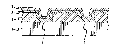
FIG. 1 is a schematic view of device according to this invention.
It comprises a silicon substrate 1, a dielectric layer 3 and a plurality of
aluminum conductors, i.e., metallizations, S on the top major surface. There
S are holes 7 in the dielectric to the silicon substrate. As depicted, the aluminum
metallizations are on both the surface of the dielectric, and in the holes 7 which
have been coated, but not totally filled, with aluminum. As can be seen, the
aluminium conductors have exposed surfaces, i.e, surfaces which do not contact
the silicon substrate or the dielectric material. Deposited on the
'' `
t 3341 58
-- 4
exposed surfaces of the aluminum are refractory material
coatings 9. As can be seen, the refractory material
covers the exposed surfaces of the aluminum runners on the
dielectric as well as the three exposed surfaces of the
aluminum within the holes. It is understood by those
skilled in the art that the aluminum is used to
electrically contact devices which form the individual
components of the integrated circuit but are not shown for
reasons of clarity. The structures depicted comprise
aluminum features which are covered on their otherwise
esposed surfaces by conducting refractory material. These
structures are conveniently referred to as encapsulated
bimetallic structures and have several advantages as
compared to prior art structures. First, as the
refractory material surrounds the aluminum features on
three sides, there will be no hillocks on either the
vertical or the horizontal surfaces of the aluminum. It
will be appreciated by those skilled in the art that the
refractory overlay prevents stress relief in the aluminum
metallization through hillock formation. Second, the
hardness of the refractory materials eliminates the
possibility of scratching the aluminum and thus impairing
the electrical or chemical characteristics of the
metallization. Of course, as will be appreciated by those
skilled in the art the refractory material is relatively
immune to scratches. Third, any electrical problems that
might arise due to the electromigration of aluminum are
greatly reduced or eliminated because if voids do occur in
the aluminum runners, the overlying refractory material
has sufficient electrical conductivity so that the desired
electrical current can flow through the bimetallic
structure. Fourth, due to the nature of the deposition
process and the resulting excellent surface coverage,
local thinning, such as those present in the window, do
not occur.
A similar passivation technique using a
dielectric will often cause hillocks to form before there
~ 5 - 1 3~4~ 58
is significant dielectric deposition due to the relatively
high deposition temperature. Additionally, there will be
no protection against electromigration.
The bimetallic structures are conveniently
S formed by a low temperature chemical vapor deposition
process. It is noted that the selective deposition of the
refractory material proceeds, and encapsulates the
aluminum on three sides, without a lithographic step. Low
temperatures are desirably used as they do not lead to
10 hillock formation. The method will be described by
explicit reference to the deposition of tungsten on
aluminum. Steps well known to those skilled in the art
will not be described. After appropriate processing, a
dielectric layer is deposited on the silicon and patterned
15 as desired. An aluminum layer is then deposited and
patterned. Tungsten is now deposited. Typical
constituents for the chemical vapor deposition of tungsten
are hydrogen and WF6. The resulting reaction leads to the
deposition of tungsten on the exposed aluminum surfaces.
20 It is believed that the reaction proceeds more
expeditiously through a surface activation mechanism with
aluminum and within a restricted temperature range
proceeds selectively, i.e., only on the exposed aluminum
surfaces. Therefore, there is little or no deposition of
25 the refractory material on unwanted surfaces.
It has been found that temperatures within the
range from approsimately 280 to 350 degrees C are
desirable. Temperatures below 280 degrees C may be used
but the deposition rate becomes undesirably slow.
30 Temperatures above 350 degrees are undesirable because
hillocks may begin to form. On l,um thick Al runners, a
deposition temperature between 280 and 300 degrees C was
used. The flow rates were 10-120 and 3000 cc/min for WF6
and }12, respectively. The pressure was O.S Torr.
35 Deposition times between 15 and 30 minutes resulted in
tungsten thicknesses between 500 and 1000 Angstroms. The
remainder of the processing sequence is similar to a
~ - 6 - l 334 1 58
conventional processing sequence through the contsct bake,
final in process and passivation steps. Details will be
readily known to or easily ascertained by those skilled in
the art and thus need not be described in further detail.
The thickness of the tungsten is desirably
between 500 and 1000 Angstroms although the precise
thickness is not critical. As twice the thickness of
tungsten is deposited in the space between lines, thick
films may lead to shorting between finely spaced lines.
It will also be appreciated that the lines are both wider
and closer together than they were before the tungsten was
deposited. The narrower spacing was obtained without
either etching or lithography.
In addition to the deposition of tungsten,
deposition of other materials is contemplated. For
example, Mo, Ta or Ti may be deposited on the aluminum
surfaces. Use of conductors other than pure aluminum is
also contemplated. For example, the presence of other
elements, e.g., silicon, in minor amounts is contemplated.
Use of Al based alloys is also contemplated. Also, use of
other metals, e.g., Mo, is contemplated. Additionally,
the bimetallic structure may comprise two layers of the
same metal but with different 8rain structure. For
example, sputtered tungsten might be deposited first
followed by chemical vapor deposition of tungsten.
Multilevel interconnects are also contemplated.
A schematic representation of a multilevel interconnect is
depicted in FIG. 2. Numerals identical to those used in
FIG. 1 represeDt identical elements. In addition the
structure previously depicted, a second dielectric layer
ll is also present and has a plurality of opening 13 which
expose a surface of refractory material 9. That is, the
second dielectric layer has been patterned. Deposited on
refractory material 9 is a layer of aluminum 15 which, in
turn, is covered on its exposed surfaces by a layer of
refractory material 17. Special attention is drawn to the
top right end where covering of the end surface of the
~ 7 ~ ~ ih ~ 4
aluminum is clearly depicted.
The refractory material is typically the same as that used for the
previous layer of refractory material and is deposited by an identical
technique. The dielectric materials are typically glass.
The etch used to pattern the aluminum etches the aluminum but
not the refractory material. There is thus significantly greater
tolerances, as correspond to prior art devices, in aligning connecting
aluminum lines as there is no danger of the etch removing the first
level metallization. FIG. 3 shows a structure having a first level
metallization 31, dielectric 33 and second level metallization 35. If, as
in prior art structures, both metallizations were aluminum, etching the
second metallization would also result in etching the first level
metallization. However, the refractory material in the first metallization
stops the etch. A top view of a two level interconnection is depicted
in FIG. 4. The first level metallization is 41, the second level
metallization 43, and they are connected via window 45.
Another view of the encapsulated structure is shown in FIG. 5.
There is a dielectric layer 51 and three encapsulated bimetallic
structures on layer 51. Each structure comprises a first conductor 53
and a conducting refractory material 55 which covers the exposed
surfaces of the conductor to form the encapsulated structure. As can
be seen, the tolerances for the overlay of crossing lines are greatly
Increased.