Note : Les descriptions sont présentées dans la langue officielle dans laquelle elles ont été soumises.
1335609
72430-86
COMMUNICATION SWITCHING ELEMENT
The present invention relates to a communication
switching element with buffer means associated with a plurality of
signal inputs and signal outputs.
In such known switching elements buffer means can
generally be associated with the signal inputs and/or with the
signal output. In case they are associated with the signal
inputs, when several signals arrive at a same signal input and
have to be transmitted to a same signal output, the corresponding
input buffer means may only be emptied at the signal transmission
speed used on this signal output. This means that the following
signals also arriving at this signal input and to be transmitted
to another signal output have to wait for the completion of the
transmission of the above preceding signals prior to being
transmitted to their destination signal output even if the latter
is not used.
In the switching element known from Belgian Patent No.
904,100 published on July 24, 1986 and used in an Asynchronous
Time Division (ATD) packet or cell switching system, buffer means
associated with the signal outputs are preferred to avoid such
input saturation. However, it requires at each of its signal
outputs relatively large buffer means able to store signals
simultaneously transmitted by all its signal inputs. Moreover, in
order to be able to accept the signals from all the signal inputs,
this known switching element operates at a speed or bitrate equal
to the sum of the bitrates at which these signals are supplied at
their respective signal input. As a result, the complexity of the
element is increased.
A solution to reduce this switching speed and
accordingly to decrease the complexity of the switching element
which has been proposed consists in subdividing each of the input
signals into a number of parts, particularly sub-packets in an ATD
system. Thus, the switching speed of the element is also divided
by the same number. However, additional circuits required to
'~
- 1335609
72430-86
realise such subdivision and to combine these parts into an output
signal also contribute to the complexity of the switching element.
In the article: "Packet Switching Interconnection
Networks for Modular Systems" by D.M. Dias et al published in
IEEE - COMPUTER of December 1981, pages 43 to 53, and more
particularly on page 45 thereof, delta networks are considered
wherein the links between stages of a packet switching network
contain data buffers organized as first-in-first-out queues and
each able to hold one or more packets. In this way the two signal
inputs and the two signal outputs of a binary switching element
part of an intermediate stage are each associated with such a
buffer. Nevertheless, blocking can still occur for such a
switching element when the buffer at one of its output terminals
is full.
In the article "THE KNOCKOUT SWITCH: A SIMPLE, MODULAR
ARCHITECTURE FOR HIGH-PERFORMANCE PACKET SWITCHING" by Y.S. Yeh et
al published in the proceedings of ISS '87 pages 0801 to 0808 as
well as in the European patent application by the same inventors
published under No. 0256702, a so-~alled N-input, N-output
"knockout" packet switch uses N output interface units, each with
N
_ 3 _ 13~S609
packet filters associated with the N signal inPuts, a
concentrator which achieves an N to L concentration, with
L<YN, and an output buffer in order to have a lost packet
rate as small as desired. However, if more than L
packets or cells for the same signal output arrive
simultaneously on the signal inPUts, the extra packets
are lost, even at a low transmission rate. Moreover, the
modularity advantage of this known system increasing with
the size thereof, it will preferably be used in large
switching sYstems.
An object of the present invention is to provide a
new switching element offering advantages over the known
solutions including versatility in the ways it can be
used.
According to the invention, this object is
achieved due to the fact that a connection between any
predetermined pair of signal input and signal output uses
distinct buffer means PermanentlY dedicated to said Pair.
In this way, a switching element is obtained
wherein all the signal inputs are simultaneously able to
transfer their input signals to the dedicated buffer
means used. Hence, the speed of transmission of the
signals between an input and an outPut never needs to
exceed the speed of the input signals and thus no
additional speed reduction circuit is required.
Moreover, because each signal outPUt uses a plurality of
buffer means which are each dedicated to a distinct
signal input and onlY receive signals therefrom, the size
of these buffer means may be relatively small.
Another characteristic feature of the Present
invention is that signals transferred from any of said
signal inputs to any of said signal outputs via said
buffer means are digital signals grouped in cells having
a header indicative of the destination signal output
thereof.
1335609
It is to be noted that in the above mentioned
known switching elements the cells or packets stored in
the output buffers means may only exit therefrom in the
order of their arrival therein. This means that cells
5 transmitted to a signal output from a signal inPut having
a high cell output rate will raPidlY fill the
corresponding output buffer means and may cause the loss
of cells, e.g. these coming from other signal inputs, due
to the overflow of the output buffer means.
Another object of the present invention is to
provide a switching element of the above known type, but
wherein the probability of cell loss is reduced.
According to the invention this other obiect is
achieved due to the fact that the switching element
I5 includes a plurality of priority circuits each
interconnecting the buffer means of a respective
associated set and each allowing said transfers one at a
time from the buffer means of said associated set which
is coupled to a distinct signal output, and that each of
said priority circuits is constituted by a token ring
wherein a priority indicating token signal is
successively passed to the buffer means of the associated
set to allow the one receiving said token signal to
transfer at least one cell to the signal output
?5 associated in common to the buffer means of said set
prior to passing said token signal to another buffer
means of said set.
In this way, all the output buffer means
associated to a same signal outPUt are emptied in
30 sequence so that the above risk of cell loss is reduced.
Still another characteristic feature of the
present invention is that each of said token rings
includes means to detect the degree of filling of the
buffer means of the associated set in order to pass said
35 token signal in priority to the buffer means of said set
1335609 72430-86
having the highest degree of filling.
This reduces even more the risk of overflow of the
buffer means, i.e. to lose cells.
Another general problem with switching elements such as
the known ones mentioned above, is that it is not easy to
distribute an input cell to more than one signal output, i.e. to
perform point-to-multipoint transmission (multicast or broadcast
connections). Indeed, the input cell has then to be copied
several times and the header of these copies has to be changed in
order to transmit each cell to the corresponding destination
signal output, this requiring additional complex circuits.
Still another object of the present invention is to
provide a switching element of the above known type but wherein
point-to-multipoint transmission is facilitated.
According to the invention, this other object is
achieved due to the fact that each signal input is coupled to an
associated second set of buffer means via a common input data bus
and via a selection bus to select the buffer means of said
associated second set into which a cell supplied to said common
input data bus has to be loaded.
In this way, an input cell is automatically copied and
loaded into all the buffer means selected by the selection bus and
associated to the respective signal outputs participating in the
point-to-multipoint transmission. Moreover, identical cells, i.e.
with a same header, are transmitted to the different signal
outputs.
~,.'~ '
13 3 5609 72430-86
The invention may be summarized, according to one
aspect, as communication switching element for transferring
digital signals, grouped in cells, from a plurality of signal
inputs to a plurality of signal outputs, said switching element
comprising: a plurality of buffer means each associated with and
permanently connected between a different pair of one of said
signal inputs and one of said signal outputs to thereby provide a
corresponding plurality of transfer paths from each signal input
to each signal output, said plurality of buffer means being
organized into a plurality of distinct first sets of buffer means
with each of said first sets being associated with a different one
of said signal outputs and with each of said signal outputs being
connected in common with all of its thus-associated buffer means,
and a plurality of token ring priority circuits each interconnec-
ting a different respective first set of said buffer means, where-
in each of said priority circuits passes a respective priority in-
dicating token signal in a predetermined priority sequence to all
the buffer means in its respective first set of buffer means, to
thereby allow at least one said cell to be transferred to the re-
spective signal output from a higher-priority buffer means receiv-
ing said respective priority indicating token signal prior to said
token signal being passed to a lower-priority said buffer means of
said respective first set, wherein each of said token ring
priority circuits further comprises means to detect the degree of
filling of each of the buffer means of the associated first set in
order to pass said token signal in priority to the buffer means of
said first set having the highest degree of filling.
5a
-- 133~609
72430-86
According to another aspect, the invention provides
communication switching element for transferring digital signals,
grouped in cells, from a plurality of signal inputs to a plurality
of signal outputs, wherein each of said cells has a header
indicative of its destination, said switching element comprising:
a plurality of buffer means each associated with and permanently
connected between a different pair of one of said signal inputs
and one of said signal outputs to thereby provide a corresponding
plurality of transfer paths from each signal input to each signal
output, said plurality of buffer means being organized into a
plurality of distinct first sets of buffer means with each of said
first sets being associated with a different one of said signal
outputs and with each of said signal outputs being connected in
common with all of its thus-associated buffer means, said buffer
means also being organized into a plurality of distinct second
sets each coupled to a different one of said signal inputs, a
plurality of token ring priority circuits each interconnecting a
different respective first set of said buffer means, wherein each
of said priority circuits passes a respective priority indicating
token signal in a predetermined priority sequence to all the
buffer means in its respective first set of buffer means, to
thereby allow at least one said cell to be transferred to the
respective signal output from a buffer means receiving said
respective priority indicating token signal prior to said token
signal being passed to another said buffer means of said
respective first set, a plurality of input data buses each coupled
to a respective second set of said buffer means and itsrespective
5b
r
-
1 3 3 5 60 9 72430-86
signal input and a plurality of selection buses each associated
with a respective said input data bus and coupled to its
respective second set of said buffer means for selecting a buffer
means of said respective second set into which a cell supplied to
its respective signal input will be loaded, and a plurality of
receiver means, each interconnecting a respective signal input to
its respective input data bus and to its respective selection bus,
for transferring said cells received at said respective signal
input to said respective input data bus and for supplying to said
respective selection bus a respective selection signal to select
at least one of said buffer means of the respective second set,
wherein each of said receiver means includes conversion means to
convert cells received in a serial way at the serial inputs into
parallel signals prior to transmitting them to the corresponding
input data bus, and a respective cell buffer means to receive a
cell with its header from said signal input and coupled to a
respective routing table for substituting a new header as a
function of said received header, said cell with said new header
being then transmitted by said cell buffer means to said input
data bus.
The above mentioned and other objects and features of
the invention will become more apparent and the invention itself
will be best understood by referring to the following description
of an embodiment taken in conjunction with the accompanying
drawings wherein:
1335609
-- 6
Fig. 1 is a schematic representation of a
communication switching element SE according to the
invention;
Fig. 2 shows an examPle of use of the switching
element SE of Fig. 1 as a module of a 16 x 16 switching
network; and
Fig. 3 shows a receiver port RP(m) of Fig. 1 in
more detail.
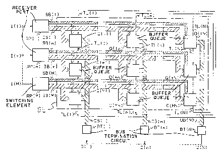
The communication switching element SE shown in
Fig. 1 forms part of a communication switching network
wherein a plurality of such elements are interconnected
in a modular way and of which an example will be given
later. Each switching element SE is able to switch fixed
length packets or cells of digital signals transmitted
according to Asynchronous Transfer Mode (ATM~, previously
called Aynchronous Time Division (ATD), techniques from a
plurality of M signal inputs I(l) to I(M), coupled
thereto via respective like receiver ports RP(l) to
RP(M), to a Plurality of N signal outputs 0(1) to O(N) to
which the element is coupled via respective like bus
termination circuits BT(l) to BT(N). A description of
the structure and the operation of a receiver port, saY
RP(m) with m being an integer between 1 and M, will be
given later by making reference to Fig. 3. Any bus
termination circuit, say BT(n) with n being an integer
between 1 and N, performs a buffering function and, if
required, a parallel-to-series conversion of the cells
supplied to it. Each cell comPriseS for instance 35
bytes of which 3 bytes are used as a header containing 2
bytes or 16 bits constituting a virtual circuit number, 5
bits for error checking and correction and 3 spare bits,
and of which the 32 remaining bytes constitute an
information field.
The switching element SE includes M x N buffer
means or queues arranged in a matrix of M rows Q(ll~ to
- 1335609
-- 7
Q(lN); ...; Q(ml) to Q(mN); ...; Q(Ml) to Q(MN) and N
columns Q(ll) to Q(Ml); ... Q(ln) to Q(Mn); ...; Q(lN) to
Q(MN). Each of these queues Q(ll) to Q(MN) is for
instance constituted by a first-in-first-out (FIFO)
memory able to store, e.g., 10 cells of 35 bytes. Each
of the M receiver Ports RP(l)/(M), e.g. RP(m), is
connected to a respective m-th row comprising a set of N
queues Q(ml) to Q(mN) through an associated 8 lines
common inPut data bus IB(m) and an associated N lines
selection bus SB(m) with each of these N lines associated
to a distinct one of the N columns of queues. Each of
these N columns, saY the n-th, comprises a set of M
queues Q(ln) to Q(Mn) and is connected to a resPeCtive
bus termination circuit BT(n) by an associated 8 lines
common output data bus OB(n). The receiver port RP(m)
associated to the sets of N queues of an m-th row is able
to convert the cells received, e.g., in a serial way on
its signal input I(m) into a succession of parallel bytes
and applY them to anyone of the N queues of the set of-
this m-th row via the associated input data bus IB(m).
One or more queues into which a cell has to be loaded are
selected by means of the lines of the selection bus SB(m)
respectively associated to the sets of columns to which
these queues belong. A Point-to-POint transmission is
thus performed when only one column, i.e. one queue, is
selected, whilst a point-to-multiPoint transmission, also
called multicast, takes Place when more columns, i.e.
more queues of a same row, are selected as will become
clear later. On the other hand, multiPoint-to-Point
transmission, also called concentration, may be performed
when several queues of a same column are selected by
different selection busses.
All the queues Q(ln) to Q(Mn) of a set of a same n
th column are further interconnected by a PrioritY
circuit constituted by a token line TL(n) which is
I335609
connected in a ring and wherein a token signal is
transmitted between the interconnected queues according
to an algorithm described later and indicating the queue
having transmission Priority as well as the number of
cells this queue is allowed to transmit to the
corresponding bus termination circuit BT~n) via the
output data bus OB(n).
Due to the modularity of the switching element SE,
all the queues Q(ml) to Q(mN) of a same m-th row or all
the queues Q(ln) to Q(Mn) of a same n-th column may be
arranged for instance on a same chiP of integrated
circuits and these chips or modules maY be easily
interconnected. As a consequence, the number M of signal
inputs of an existing M x N switching network may be
increased just by adding rows of queues. Similarly, the
number N of signal outputs of an existing M x N switching
network maY be increased bY adding columns of queues.
The only restriction in this last case is the number of
selection lines constituting the selection bus SB.
Indeed, as mentioned above, each queue of a row is
associated to a distinct line of this selection bus SB.
An example of a 16 x 16 switching network wherein
switching elements SE each comPrising 4 x 4 queues
grouped on a same chiP are used is shown in Fig. 2.
This switching network comprises 4 rows of 4 such
switching elements SE(ll) to SE(14); ... ; SE(41) to SE
(44). The left hand side of Fig. 2 shows 16 receiver
ports RP(l) to RP(16) all connected to a Processor PR via
a bidirectional bus ADP and having respective signal
inputs I(l) to I(16). For each receiver port the input
data bus and the selection bus are rePresented together
by a single line. For instance SB(1~+IB(l) is associated
to the receiver Port RP(l). The outPUt data busses OB(l)
to OB(16) connected to the respective bus termination
circuits BT(l) to BT(16) are also each represented by a
1 33$609
single line. The switching elements of each of the
columns SE(ll) to SE(41); ... ; SE(14) to SE(44) are
interconnected via a respective token line TL(l); ... ;
TL(4). Each of these token lines is connected in a ring,
i.e. that the token line output of a bottom switching
element, e.g. SE(41), is connected to the token line
input of a toP switching element, e.g. SE(ll).
Depending on thé application different algorithms
may be used to control the token lines.
The most straightforward one consists in passing
the token signal successively to all the queues of a same
column :
- if a queue is not empty when receiving the token
signal it has priority to transmit one cell to the
associated output data bus and holds the token signal for
the duration of the transmission of this cell;
- if the queue is emptY, the token signal is immediately
passed to the next queue in the column so that no time is
wasted.
A variant of the above is to make the number of
cells which are allowed to be transmitted by the priority
dependent on the degree of filling of this queue. This
reduces the danger of cell loss bY queue overflow.
In another solution the token ring is constituted
by a ring of status lines (not shown) interconnecting all
`;~he queues of a same column and indicating the one
having the highest degree of filling. In order to
decrease the danger of cells loss the token signal is
given in PrioritY to this queue storing the highest
number of cells.
The receivèr port RP(m) with its signal inPut
I(m), its input data bus IB(m) and its N-lines selection
bus SB(m) is shown in more detail in Fig. 3. It includes
a synchronisation circuit INC which has the signal input
I(m) and is connected by a data bus Bl to a first input
- 1335609
-- 10 --
of a multiPlexer MXI and bY a control line Ll to a
controller CT. INC is also able to perform
series-to-parallel conversion if the internal width of
the data busses, e.g. the bus Bl, is wider than that of
the input line, by which INC is connected to the signal
input I(m), i.e. for instance when the cells are received
in a serial way on this signal inPut I~m) as mentioned
above. The output of the multiplexer MXI is connected by
a data bus B2 to a single cell buffer SCB which is itself
connected, in series with a header check and correction
circuit HC, to a routing circuit R0. The routing circuit
R0 is connected to a first terminal of a
multiplexer/demultiplexer MDC bY a bidirectional bus B3.
A second terminal of this multiplexer/demultiplexer MDC
is connected to a routing table RT bY a bidirectional bus
B4 whilst a third terminal of MDC is connected to a first
terminal of another multiplexer/demultiplexer MDP via a
bidirectional bus B5. The multiplexing part of MDC has
inputs constituted bY the above first and third terminals
and an output constituted by the above second terminal,
whilst the demultiplexing part of MDC has an input
constituted by the second terminal and outputs
constituted by the first and third terminals. The single
cell buffer SCB is also connected via a bus B6 to the
input of a demultiplexer DX0 which has a first output
connected to the input data bus IB~m), whilst the routing
circuit R0 is directly connected to the selection bus
SB~m) and controls the selection input of this
demultiplexer DX0 via a control line L2. The controller
CT receives a clock signal via a line CK and control
signals from the series-to-parallel converter and
synchronization circuit INC via the line Ll and from a
processor PR ~shown in Fig. 2) via a selection line CS
(Chip Select). This controller CT controls the operation
of the above multiplexer MXI and the
33s609
multiplexers/demultiplexers MDC and MDP via the
resPective selection lines L3, L4 and L5. As shown in
Fig. Z, the processor PR is connected to all the receiver
ports of a switching network by a bidirectional data and
address bus ADP which is connected to a second terminal
of the multiplexer/demultiplexer MDP. MDP has a third
terminal connected via a bus B7 to an input cell buffer
CBI which is itself connected to a second input of the
multiplexer MXI via a bus B8. A second outPUt of the
demultiplexer DX0 is connected to an output cell buffer
CB0 via a bus B9 and this output cell buffer CB0 is
connected to a fourth terminal of the
multiplexer~demultiplexer MDP via a bus B10. The
multiplexing part of MDP has inputs constituted by the
above first and fourth terminals and an output
constituted by the above second terminal, whilst the
demultiplexing Part of MDP has an inPut constituted bY
this second terminal and outputs constituted by the first
and third terminals.
The cells supplied in a serial way to the
series-to-parallel converter and synchronization circuit
INC are converted therein into sets of e.g., 8 parallel
bits which are then transmitted and latched into the
single cell buffer SCB via the multiplexer MXI. When an
error in the synchronization of an incoming cell is
detected by the series-to-Parallel converter and
synchronization circuit INC, a signal is transmitted via
the line Ll to the controller CT which is able to execute
the appropriate action. When a cell is stored in SCB the
~ 30 header thereof is sent to the header check and correction
circuit HC for testing its validitY and for correcting
some types of recoverable errors. This header is then
transmitted via the multiplexer/demultiplexer MDC to the
routing table RT which contains a table wherein headers
of cells and associated routing information are stored.
- 12 - 1335609
In the routing table RT the incoming header acts as a
pointer for this table and is translated into an outgoing
header which is returned, together with routing
information, to the routing circuit R0. The outgoing
header is directlY transmitted to the single cell buffer
SCB where it is substituted for the incoming header and
the updated cell is then transmitted on the input data
bus IB(m) via the demultiplexer DX0. Simultaneously, the
routing information constituted, e.g., by an N-bits
binary word is transmitted to the routing circuit R0
which applies it, one bit per line, to the N-lines
selection bus SB(m) and at the same time activates the
selection line L2 of the demultiplexer DX0 which
accordingly selects its first output. Each line of the
selection bus SB being connected to a distinct queue, the
value of the bit transmitted on this line indicates
whether the corresPonding queue is selected (bit=l) or
not (bit=0) for receiving the cell then transmitted on
the input data bus IB(m).
The contents of the routing table maY be updated
by the processor PR which has a direct access to it via
the busses ADP, B5 and B4 and the
multiplexers/demultiplexers MDP and MDC. Furthermore,
the processor PR may transmit a cell on the input data
bus IB(m) or receive a cell via the signal input I(m) as
will be described below. In case of a cell to be
transmitted by the processor PR to the input data bus
IB(m), this cell is loaded by PR in the input cell buffer
CBI via the bus ADP, the multiplexer/demultiplexer MDP
and the bus B7. As soon as no cell is transmitted by the
parallel-to-series converter and sYnchronization circuit
INC on the bus Bl, the cell stored in the input cell
buffer CBI is transmitted to the single cell buffer SCB
via the busses B8 and B2 and the multiplexer MXI. From
there this cell follows the same way as those coming from
- 13 - 1335609
the input I(m). On the other hand, a cell destined to
the processor PR follows the same waY as a cell going to
the input data bus IB(m) but in the demultiPlexer DXO it
is routed to the output cell buffer CBO via the bus B9.
From the outPUt cell buffer CBO this cell is transmitted
to the processor PR via the multiplexer/demultiplexer MDP
and the busses B10 and ADP.
A point-to-multipoint transmission of cells is
largely facilitated by the structure of the switching
element SE and its associated receiver Ports RP(l) to
RP(M). More particularly, contrary to a switching
element wherein point-to-multipoint transmission is onlY
possible by making copies of the cell to be transmitted
and by changing the headers of these copies to address
corresponding signal outputs, the present element SE
operates in a different way. Indeed, the header of a
cell is here not directlY used to address a signal output
so that this header needs not be changed for each signal
output particiPating in the multipoint transmission.
Instead, in this switching element SE the correct signal
outputs O(l) to O(M) are solely selected by means of
their respective associated lines of the selection bus
SB. These lines are activated (bit=l) when the
associated signal output is selected, and de-activated
(bit=0) otherwise. As a consequence, each cell
transmitted by a receiver port RP(m) on the input data
bus IB(m) is copied into all the selected queues
Q(ml)/(mN) and from there to all the selected signal
outputs O(l)/(N).
While the principles of the invention have been
described above in connection with specific apparatus, it
is to be clearly understood that this descriPtion is made
only by waY of example and not as a limitation on the
scope of the invention.