Note : Les descriptions sont présentées dans la langue officielle dans laquelle elles ont été soumises.
1 336725
73834-14
BACKGROUND
Thls lnventlon relates to slgnal processlng technlques
and clrcults whlch remove an unwanted segment from a slgnal and lt
has partlcular applicatlon to derlvlng such a slgnal for drlvlng
servo-mechanlsms where the unprocessed slgnal contalns undeslrable
portlons. It ls particularly useful for slgnals ln whlch the
deslred portlon of the slgnal contalns a leg of relatlvely mlld
slope and a rapld leg of relatlvely large opposlte slope. Thls
clrcult has partlcular appllcatlon to derlvlng useful veloclty
lnformatlon from the "trl-phase servo patterns" as descrlbed
herelnafter.
Thls speclflcatlon assumes some famlllarlty wlth the
constructlon of magnetlc dlsk drlve data storage systems and means
for generatlng and uslng servo lnformatlon from coded lnformatlon
on the dlsk medla but lts teachlngs can be applled to analogous
art as well.
In the speciflc system for whlch this invention was
developed, removlng unwanted slgnal portions and dlfferentlatlng
thls slgnal wlth respect to a reference voltage provldes a
contlnuously accurate, useable, llnear veloclty slgnal
correspondlng to the radlal speed and dlrectlon of the servo
reading head (whlch provldes the orlglnal lnput for thls slgnal).
Where thls readlng head ls mechanlcally (or otherwlse) llnked to
other heads travelllng over data dlsks the lnformatlon ls dlrectly
indlcatlve of thelr radial speed also.
6082-243
1 336725
An example of a system for generating a continuous servo
signal is printed in U.S. Patent No. 4,130,786 issued to Jacques.
The Jacques' patent uses two-phase signals to generate a saw-
tooth waveform and adds this saw-tooth waveform with a staircase
waveform also generated by reference to the two-phase signal.
The result is a continuous slope linear signal.
It has also beenkncwn to charge a capacitor in a circuit and
employ the discharge to smooth a signal, as for example in U.S.
Patent No. 4,584,559, issued to Penny. Penny does not provide
for differentiation of the input signal. In addition, the Penny
circuit contains offset errors contributed by two op amps (main-
ly from 56 and 52 with minor contribution from 48). The present
invention only contains offset errors contributed by one op amp
(Ul-A, with minimum contribution from Ul-B).
1 336725
SUMMARY OF THE INVENTION
This invention produces a differentiated signal representing a
velocity with a stair-step after a reset interval proportional
to the relatively slower slope of a saw-tooth wave signal which
is the input signal. In the context of the device for which it
was developed, it synthesizes a useful differentiated signal
during ~reset~ intervals.
The input signal builds a voltage level VH substantially
representing the current through an input capacitor and is
located between two input resistors on the signal voltage input
line, presenting the signal's time varying voltage for
processing (in this case by differential amplifier also called
an op amp, which yields a signal representing a difference from
a reference voltage). Between the occurrences of the unwanted
signal portion (in this case between the reset intervals) a
second op amp receiving the VH voltage as positive input
creates a voltage level to be stored by a second (storage)
capacitor which will then hold a voltage level representative
of the input signal current.
During unwanted signal portions (in the preferred embodiment),
the voltage level of the input signal changes rapidly.
A ~reset~ signal switches the output of the second op amp to a
circuit having an amplifier gain adjusted to produce the
appropriate output voltage level from the representative
_ ~ 33672~ 73834-14
voltage level input to lt vla the second op amp. This gain
ad~usted output ls provlded to cover the input slgnal untll the
reset slgnal pulse ls over.
To use an op amp for dlfferentlatlon the op amp would
have lts negatlve lnput tled to its output vla a reslstor and the
lnput slgnal llne would have a capacltor ln lt. For thls clrcult,
reslstors R2 and R3 and a capacltor C2 located between them and
tylng the reference voltage llne to the other slde of C2, they
then act as an addltlonal fllter to prevent saturatlon of Ul-A on
the occurrence of hlgh noise signals.
The reset slgnal ls derlved from a trl-phase servo
pattern (dlscussed later) and ls responslve to lt. It ls
trlggered upon the crosslng polnts of the upward-golng slopes of,
for example, the flrst of the three trl-phase slgnals wlth the
downward-going slope of the thlrd. The clrcult could, of course,
be used ln any devlce ln whlch a rapld slope transltlon on an
lncomlng slgnal must be removed from lnfluenclng the processed
outgolng slgnal. For any appllcatlon, lt ls assumed that the
unwanted portlons wlll have some lnherent lndlcator of thelr
occurrence so that a reset slgnal may be derlved therefrom.
In accordance wlth a broad aspect of the lnventlon there
ls provlded a clrcult for removlng unwanted temporal portlon of a
voltage varying slgnal current lnput thereto on the occurrence of
a reset slgnal and for dlfferentlatlng the resultant corrected
slgnal wlth respect to a reference voltage provlded by one of at
least one reference voltage sources whereln sald clrcult has:
~ 3 3 6 7 2 ~ 73834-14
swltch means responslve to sald reset slgnal havlng as a
flrst lnput sald reset slgnal and havlng a second lnput and havlng
a
4a
~ 3 3 6 7 ~ 5 73834-14
first and second output, wherein sald swltch means in response
to said reset signal diverts the second input to said second
output from said first output and thence returns said second
lnput connection to said first output,
input capacitor for receiving said input signal
current,
op amp means having a positive and negative input, and
an output connected to said second input of said switch, and
having said positive input connected to receive voltage repre-
sentative of the current through said input capacitor by being
in electrical connection therewith,
storage capacitor means having one side connected to
any reference voltage and having its other side in electrical
connection to said op amp means' negative input and with said
first switch output,
a first resistor,
a feedback resistor,
an inverting amplifier means connected to receive said
second switch output, and
second op amp means for receiving the second switch
output as a corrected input signal having a negative input which
is connected through the first resistor and through the inver-
ting ampllfler means to sald second switch output and which
negative input of said second op amp means ls also in electrical
connection through said first resistor with said input capacitor
and with said positive input of said first op amp means,
4b
1 3 3 6 7 ~ 5 73834-14
a positive input connected to a reference voltage, and
which provides as output, said differentiated corrected signal,
and this output is also connected via a feedback reslstor to
said negative input.
1 33672S
BRIEF DESCRIPTION OF THE DRAWINGS
Figure 1 is a simplified diagram of the circuit employed in the
preferred embodiment.
Figure lA is a detailed diagram of the circuit of the preferred
embodiment. Where Alphanumeric indicators on this Figure which
are the same as those in Figure 1, the element indicated is or
represents the same structure or provides the same function as
the element with the corresponding indicator in Fig. lA.
Figure 2 is a graph with a set of voltage signals with respect
to time.
Figure 3 is a diagram of a typical practical differentiator.
Alphanumeric indicator correspondence with elements of
Figures 1 and lA means similar structure or function is
portrayed.
Figure 4 is a graph of a nonideal input signal.
Figure 5 is a graph of a possible ideal output signal.
Figure 6 is a diagram of a circuit for deriving the digital
pulse stream for deriving a reset signal from a tri-phase servo
pattern.
1 3 3 6 7 2 5 73834-14
Flgure 7 ls a graph of three slgnals, palrs of whlch are
related to the clrcuit of Flgure 6.
Flgure 8 on the thlrd sheet of the drawlngs, ls a graph
of an output slgnal.
Flgure 9 ls a schematlc dlagram for a clrcuit for
derlving the reset signal in accord wlth the preferred embodlment.
Flgure 10 on the sixth sheet of drawings, is a timing
diagram for use with Figure 9.
Figure 11 is a schematic vlew of a magnetlc lnformation
storage disk with servo patterns positioned thereon.
Figure 12 is an enlarged schematic view showlng a
surface portlon of the dlsk of Flgure 11.
Flgure 13 is a timing diagram corresponding to the disk
surface portion of Figure 12 illustrating the writing of servo
information on the disk.
Figure 14 is a graphical representation of the signals
generated by the servo patterns.
Figure 15 is a schematic view of apparatus illustrating
the recovery of information using the signals ln Figure 14.
Flgure 16 ls a graphlcal representatlon of dlfference
slgnals obtalned by comparlng selected palrs of the slgnals ln
Flgure 14.
Flgure 17 ls a graphical representation of summing
signals obtained by combinlng selected pairs of the slgnals ln
Flgure 14.
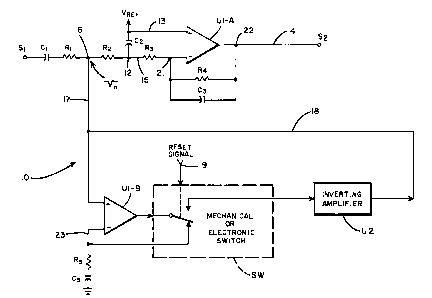
Flgure 18 shows an alternatlve embodlment of the present
lnvention.
_ 1 336725 73834-14 Note that the reference characters used ln Flgures 11-
18, if the same as ln Flgures 1-10, do not lndlcate the same ltems
as ln Flgures 1-10.
6a
DETAILED DESCRIPTION OF PREFERRED EMBODIMENT
~ 1 336725
In Fig. 1, a simplified diagram is presented detailing the
relevant features of the preferred embodiment circuit 10. (The
term ~line~ is used herein to denote electrical connection via
wire or other means.) The signal is input to the circuit 10 at
point Sl charging capacitor Cl and thence through resistors Rl,
R2, and R3 to the negative input of op amp Ul-A. The line
between resistor R3 and the negative input to op amp Ul-A is
also linked to resistor R4 and capacitor C3 which are connected
in parallel between the point 21 and point 22, on line 14.
Line 14 is the output of op amp Ul-A provided as output from
circuit 10at point S2. The positive input line 13 to op amp
Ul-A provides a reference voltage and is connected across
capacitor C2 to point 12 on the signal input line. Between
resistors Rl and R2 on the signal input line, a point 16
connects line 17 to positive input of op amp Ul-B. Line 17 is
also connected to line 18. The negative input of op amp Ul-B
is connected to ground (GNDJ through resistor R5 and capacitor
C5 (on line 23). The output of op amp Ul-B is selectively
connected between: (a), a point on line 23 between the negative
input to op amp Ul-B and resistor R5, and (b), approximate
minus one amplifier U2. The selection is governed by a reset
signal provided on line 19 to the mechanical or electronic
switch SW. On the occurrence of a reset signal on line 19, the
switch directs the output of op amp Ul-B to the approximate
-
1 3 3 67 2 ~ 6082-243
minus one amplifier U2. After the reset signal indicates that
the reset is no longer occurring, the switch is set to provide
the output of op amp Ul-B to line 23. The output of the ampli-
fier U2 is provided on line 18 to its connection to line 17.
The differentiator with hold while reset functions as fol-
lows.
The input signal charges capacitor Cl and provides a voltage
level VH at point 16 which represents the charging current ~
through Cl. (Referring briefly to Figure 3, it will be noted
that resistors R2 and R3 and capacitor C2 are additions to this
circuit which are not found in the typical practical different-
iator of Figure 3.)
Note that op amp Ul-A connected as shown will tend to stab-
ilize itself at a point where the voltage on the negative input
is brought up to the level of voltage on the positive input
(VREF). Therefore, op amp Ul-A's output voltage will tend to
be proportional to VH. It should be recongnized that because the
changes in VH may be very small (about 0.1 millivolt) any am-
bient current leakage will affect the circuit performance. This
fact must be considered in component choice, described in detail
within, with reference to Figure lA.
1 336725
~he~ voltage VH on line 17 is provided as positive input to
operational amplifier Ul-B. During the normal operation of the
circuit when the wanted portion of the signal is provided as
input on Sl and no reset signal is present on line 19, the
output of op amp Ul-B is provided to line 23 as input to the
negative input of op amp Ul-B and through resistor R5 to
capacitor C5 and to ground, or as in the preferred embodiment
may employ a 5 volt reference in place of the ground.
(Resistor R5 can provide filtering to the voltage provided to
capacitor C5, as shown, if desired.) On the occurrence of a
reset signal the mechanical or electronic switch SW transfers
the output of op amp Ul-B to the approximate minus one
amplifier U2. Thus the voltage level on capacitor C5 provides
an error voltage to the minus one amplifier U2 which provides a
voltage level equal to the voltage level on capacitor C5 on
line 18 to line 17 and to point 16, thus sustaining the voltage
level to the negative input of op amp Ul-A during the reset
interval.
A more detailed schematic diagram is provided in Fig. lA in
which the resistance and capacitance values are provided and
references made to standard industrial use numbers for
designating particular integrated circuit and other component
parts. As with Fig. 3 identical numerals correspond to the
same elements.
1 336725
~erring now to Fig. lA, a circuit lOA is provided to show the
details of the preferred embodiment circuit used in this
invention. Reference numerals in this circuit, which
correspond to reference numerals in circuit 10 of Fig. lA,
indicate a correspondence of function. Resistance,
capacitance, and voltage values may be varied in accord with
principles known to those in the art without deviation from the
inventive concepts described herein. Certain characteristics
of some of the devices pictured, however, are important to
prevent problems with ambient voltage affecting the performance
of the differentiation characteristics of op amp Ul-A. For
instance, the circuit elements designated U2 comprise a low
leakage, high output impedance inverter amplifier when not
operating so transistors Q3 and Q4, for instance, must be low
leakage transistors. The numbers 2N3904 designate transistors
of this type to one of ordinary skill in the industry.
Likewise, op amp Ul-B, designated by the industry standard
number LF412A (currently available through National
Semiconductor Corp.), is high speed op amp with high input
impedance (100 pico amp input), which will have no leakage
current to affect the operation of Ul-A, which will most likely
be on the same circuit board.
1 3 3 6 7 2 5 6082-243
Figure 4 illustrates a small segment of a possible nonideal
input signal. This signal would correspond to some portion of
the WFl waveform of Figure 2. Because the signal is originally
generated by digital circuits in the preferred embodiment, it
takes on a stairstep form as shown. Due probably primarily to
irregularities on the data disk itself, transients or spikes tl,
t2, and t3 will often be found in the preferred embodiment, non-
ideal input signal. These transients, as well as the stairstep
configuration of the input signal, will be smoothed and filtered
out by the circuit described herein. (The curve described by
numeral 40 is the signal with reference to the VREF or reference
voltage level in Figure 4.)
It must be noted that the reference voltages need not be the
same DC potential for any of the three points to which they are
introduced into the circuit, however the potential values must
be constant. A reference voltage of 5 volts for the op amp pos-
itive input worked best with the preferred embodiment to achieve
the greatest dynamic range for the power supplies used.
Figure 5 describes by curve 41 a possible ideal output sig-
nal. Segment 42 would correspond to the negative output signal
portion described by line WF3 in Figure 2.
1 336725
rh~re are flve waveforms illustrated in Fig. 2, including:
WF-1, an input signal with a negative going slope and a
positive slope transition;
WF-2, the reset signal, consisting of a series of pulses
indicating the time period for the slope transition;
WF-3, being the negative output signal provided on signal
cutput point S2 for the negative slope input WF-l;
WF-4, which is an input signal of positive slope and its
corresponding output for positive output WF-5.
All these waveform signals occur over the same length of time
and the voltage value is plotted against a voltage reference
level as illustrated by the lines marked VREF. WF1, WF2,
and WF3 may occur concurrently, and WF4, WF5, and WF2
may also occur concurrently, using this invention.
Deriving the Reset Signal
Referring now to Fig. 6, a circuit diagram is provided for
circuit 100 through which the reset signal may be derived from
1'~"
1 3 3 6 7 2 5 73834-14
the tri-phase signal's input in the preferred embodlment use of
this lnvention. Three triangle wave signals A, B, and C, are
provided on llnes 31, 32, and 33, respectively. The triangle
waves are derived from tri-phase spaced signals located in the
formatted data dlsk used wlth the prepared embodlment as descrlbed
later. Clrcult 100 of Flgure 6 provides the slgnal lnput at Sl of
Flgures 1 and lA from llne 36. A detalled representatlon of thls
output slgnal is found in Figure 8 and of the tri-phase lnput
slgnals is found at the top of Flgure 7.
Note that in Figure 7, three "bit" signals, 0, 1 and 2
(square wave signals or digital "pulses") are shown in their
radial relation to the tri-phase input signals which occur at the
same time and radial posltlon. These blt slgnals 0, 1, and 2 can
be found on output llnes B0, Bl, and B2, respectlvely. The
negatlve golng slope of each one of these three slgnals produces a
reset slgnal of a flnlte duratlon. Thls could be done wlth a
mlcroprocessor decode of the three blt pulses or, lf one ls
wllllng to accept only generatlng reset slgnals durlng the head-
ln (l.e. head movlng towards the center of the dlsk), one could
use two EXCLUSIVE-0~ gates such as gates 52 and 53 arranged and
connected as shown. The preferred
-
6082-243
1 336725
embodiment decode circuit is explained with reference to Figure
9, which generates a reset signal during rapid transition periods
in the servo position error signal, but any number of embodiments
may be constructed to accomplish this once it is understood. The
bit signals used to generate the reset signal are produced by a
circuit such as the preferred embodiment circuit 100 of Figure
6, which acts in the following manner.
The three phase signals (A, B, and C) are compared by the
three comparators U81, U82, and U83 as shown. Where the A
phase signal (on line 31) is higher voltage than the B phase
signal (from line 32), the output of non-inverting buffer circuit
U21 is "hi" and the output of inverting circuit U11 is "lo".
Otherwise, the reverse is the case. The other two comparators
and their associated inverting and non-inverting circuits func-
tion in the same way for their inputs.
Referring now to Figure 6 in which the generalized circuit
diagram employed by this invention to derive the reset signal
is shown, signals A, B, and C are input into the circuit 100 on
lines 31, 32, and 33, respectively. In Figure 7, typical sig-
nals A, B, and C, are shown with respect to a reference voltage
level VREF. One of each of the signals is fed into the
positive input of a co~arator circuit U81, U82, or U83. 1 336725
Or~ of the other of the three input signals is input into the
negative input of these same three comparator circuits. LM339
is the industry standard numerical designation for the U8
circuits used in the preferred embodiment and it is currently a
available from National Semiconductor Corp.
Each one of the input signals (A,B, and C) is also input to two
of the six analog switches U14(1 6)' to be passed through to
inverting and non-inverting differential amplifier input lines
34 and 35, respectively, to create the SPE or servo position
error signal shown in Figs. 7 and 8.
The peak input signals A, B and C input to the comparitors
U81, U82 and U83 in turn drive logic inverters Ull,
U12, and U13, and also drive logic buffers U21, U22,
and U23. The output of theses logic inverters and buffers
provide the proper switching of the analog switches U141_6.
Resistor Capacitor pairs 101,102 and 103 provide hysteresis to
the respective comparitors U81, U82, and U83 to prevent
multiple switching during noise transients which may appear in
the A, B, or C signals.
Circuit Ul9 is a differential amplifier which produces a signal
Ig-
-
` 1 3 3 6 7 2 5 6082-243
on line 36 as shown in Figure 8. The alphanumeric indicators
attached to the signal graphed in Figure 8 (for Head-in sequence)
correspond to the decimal or SPE indicators shown in Figure 7.
The outputs of the U8 circuits produced on bit lines B1, B2,
and B0, are shown in Figure 7, as 0, 1, and 2. Therefore, look-
ing at the signals in a Head-In direction in Figure 7, because
the transition or unwanted signal portion occurs between the
areas designated 6 and 2, the areas designated 3 and 1 and the
areas designated 5 and 4 (see Figure 5 and bottom of Figure 7)
and because a downward going pulse occurs at each one of these
area interfaces and because only one of the three bit signals is
hi at a downward going signal area, all that is necessary is to
fire a reset signal at a downward going pulse. Going Head-out,
each upward going pulse will signal that a reset signal is nec-
essary; i.e., that the slope transition occurs at that interface.
A microprocessor could receive these digital bit signals as in-
put and based on a program generate a reset pulse at the proper
upward or downward going transitions of each of the bit signals.
It is simplest and most efficient to think of this in terms of
two EXCLUSIVE OR gates such as 52 and 53, which will provide an
output pulse of relatively short duration in conjunction with a
digital one shot for each of the indicated transistors.
In the pre~erred embodiment, the decode of the sit signals
0, 1, and 2 is accomplished with the equivalent of three AND gates
with an ouput each to one of three flip-flops whose outputs are
OR'd together. The output of this OR would be the reset signal
for both Head-In and Head-Out orientations. In practice the re-
set signal generation is more complicated and is explained with
16
~ , 1 3 3 6 7 2 5
6082-243
reference to Figure 9, wherein a circuit 200 to accomplish this
is shown, however it should be noted that other decode schemes
are produceable and that reset signals may come from things other
than the Tri-Phase servo signal of this embodiment.
In Figure 9, a clock input, which is of a period length smal-
ler than the desired duration of the reset signal, is provided to
the circuit at input 201. The clock pulse should be a short por-
tion of the clock period. It (clock 1 - see Figure 10) is pro-
vided as the clock input to flip-flop F7. A second clock,
clock 2 provides a delayed clock to NAND gate N2, and its in-
verse is provided to NOR gate N4~
-- 1 33672~
73834-14
The output of F7 where "10" provldes the Reset Slgnal
used ln the clrcults 10 and 10A to control the swltch.
Clrcult 200 recelves the three "B" or blt outputs of
Flgure 6's Circult 100 (shown ln tlmed relatlon to each other ln
Fig. 7) as lnputs. They are provlded, lnverted and non-lnverted
as lnput to NOR gates Nl, N2, and N3, as shown. The outputs of
these NOR's are lnput to fllp-flops F4, F5, and F6. The Q-bar
output of these fllp-flops ls lnput to NAND gate NAl, whose output
ls provided as lnput to NAND gate NA2. The output of NAl also
clears flip-flop F7. NAND gate NA2 also receives the Q-bar output
of F7 and the Q-bar output of F8 as lnput, and on the NAND of
these three lnputs provldes a clear slgnal to fllp-flops F4, F5,
and F6. The D lnputs of fllp-flops F4, F5, F6, and F8 are all
tled to a "hl" slgnal or voltage level as lndlcated by the arrows
attached thereto ln the drawlng.
It should be clear that thls clrcult schematlc ln Flgure
9 and lts assoclated tlmlng dlagram of Flgure 10 only provlde for
an efflclent decode for the reset slgnal and ls not presented to
llmlt the lnventlon clalmed to thls clrcult.
The followlng descrlptlon, ln connectlon wlth Flgures 11
to 18 of the drawlngs, ls provlded to explaln ln some detall the
"trl-phase servo patterns" mentloned above.
In Flgure 11, there ls shown a magnetlc lnformatlon
storage dlsk 16 rotatable about a central axls 18 by means of a
dlsk drlve, not shown. Dlsk 16 ls a "dedlcated servo" dlsk, and
contalns no worklng data-only servo data.
Certaln parts of a magnetlc dlsk drlve are shown ln
1 336725 73834-14
Flgure 11 to lllustrate the wrltlng of lnformatlon on the upper
surface of dlsk 16 and the subsequent readlng of such lnformatlon.
These parts lnclude a read/record transducer 20. The transducer
ls mounted to a movable carrlage 22 by means of a support arm 24.
A voice coll 26, mounted to the drlve, supports carrlage 22 for
llnear movement toward and away from axls 18, thus movlng
transducer 20 radlally wlth respect to the dlsk. Typlcally,
carrlage movement and posltlon are controlled through controlllng
electrlcal current to volce coll 26. By varylng transducer radlal
posltlon and rotatlng dlsk 16 wlth a drlve motor ~not shown~,
lnformatlon may be wrltten at any deslred locatlon on the dlsk
surface.
Servo lnformatlon ls wrltten on dlsk 16 by lntroduclng
an electrlcal current I to the transducer through a flrst llne 28,
wlth transducer 20 posltloned over a selected portlon of the dlsk
surface. Transducer 20 also ls adapted to read lnformatlon
prevlously wrltten on dlsk 16, generatlng an electrlcal slgnal as
represented by voltage V ln a second llne 30. As lndlcated by a
thlrd llne 32, voltage V ls an lnput to volce coll 26. Responslve
to the V lnput, and a source of veloclty commands (not shown),
volce coll 26 elther moves carrlage 22 or malntalns lt
substantlally statlonary ln order to control the radlal posltlon
of the transducer.
Shown on part on the surface dlsk 16 are slx servo
groups, Rl-R6, radlally and unlformly spaced apart from one
another and generally concentrlc about axls 18. Each group can be
a separate rlng, or all groups can be part of a contlnuous splral
18a
1 3 3 6 7 2 5 73834-14
group, there belng a selected index or angular posltlon on dlsk 16
as a cutoff point between a group and the next subsequent group.
The types of servo pattern groups, labelled A, B and C
respectlvely, are written on dlsk 16 durlng formatting, and need
not be rewritten durlng normal operatlon. Servo pattern groups Rl
and R4 contain only type A servo patterns, servo pattern groups R2
and R5 contain only type B servo patterns, while servo pattern
groups R3 and R6 contaln servo patterns only of type C. It should
be understood that thls sequence of A, B and C is repeated for the
deslred number of servo tracks on dlsk 16, typlcally ln the
hundreds or thousands.
Servo patterns A, B and C are further arranged angularly
in sectors and radially in groups, such as represented by radll 1-
7. Radll 1, 4, and 7 contaln only type A servo patterns, radll 2
and 5 contaln only type B patterns, while radli 3 and 6 contaln
only type C patterns. This A, B and C sequence ls repeated
through the entlre revolutlon of disk 16. Servo patterns A, B and
C thus are radially and angularly offset from one another, and
arranged ln a repeating sequence both in the radial and angular
dlrectlons. Each indlvldual A, B and C pattern wrltten by
transducer 20 can be also read by transducer 20 at a later tlme
for purposes of indicting radlal positlon of arm 22 on disk 16.
As is well understood by those skllled in thls art, a transducer
20 when writlng on a disk 16 produces individual A, B and C
patterns whose physical width, whlch ls measured along a dlsk 16
radius (vertically ln Flgure 12), ls related to the width of the
flux gap of transducer 20 itself, also measured along a radlus and
18b
- 1 336725 73834-14
usually approxlmately equal to the physlcal wldth of the flux gap
of transducer 20. Durlng readlng the transducer produces a slgnal
whenever a pattern passes beneath lt. The strength of that slgnal
ls approxlmately proportlonal to the radlal wldth of the portlon
of the transducer 20 flux gap beneath whlch the pattern sweeps.
Thus, if the pattern sweeps beneath 40% of the gap width, the
level of the signal generated by the wlnding of transducer 20 wlll
be approximately 40% of the level generated by a pattern sweeplng
beneath all of the wldth of the transducer 20 flux gap. Thus, the
slgnal level from transducer 20 ls a measure of lts allgnment wlth
a partlcular pattern. In general, the apparent wldth of a
transducer 20 flux gap when readlng substantlally equals that when
writlng, and both are substantlally equal to the physlcal wldth of
the transducer ltself.
Each group of consecutlve radll contalnlng A, B and C
servo patterns forms one of a serles of substantlally ldentlcal
data frames F. One such frame Fl, and a portlon of the followlng
frame F2, ls shown ln Flgure 12, which ls an enlargement of a
selected portlon of the surface of dlsk 16.
At the leadlng edge of frame Fl ls a column of
overlapplng code blts Cl, C2, C3, C4 and C5 correspondlng to servo
tracks Rl through R5. Spaced angularly from the code bits ls a
column of sync blts Sl, S2, S3, S4 and S5. Nelghbourlng code and
sync blts overlap one another, and are sllghtly angularly
dlsplaced from one another because lt ls not posslble wlth current
technology to allgn them perfectly.
The code blts are used to lndlcate an lndex (a speclflc
18c
~,
1 3 3 6 7 2 5 73834-14
angular location) and to lndlcate the innermost and outermost
servo tracks. For example, an index can be marked by
lntentlonally avoldlng wrltlng code blts, as lndlcated at C12 and
C13. Sync blts contrlbute to establlshlng the level for automatlc
galn control (AGC), and they enable dlfferentlatlon between servo
patterns A, B and C based on thelr dlfference ln phase or angular
locatlon.
Each data frame conslsts of 50 equal dlvlslons. The
lead edge of each servo pattern A ls approxlmately seven dlvlslons
dlstant from the tralllng edge of lts assoclated sync blt (e.g.,
Sl or S4). The leadlng edge of each servo pattern B ls separated
from the tralllng edge of lts correspondlng sync slgnal by
approxlmately elghteen dlvlslons, whlle the dlstance between the
leadlng edge of each servo pattern C and the end of lts assoclated
sync blt ls twenty-nlne dlvlslons. The dlfference ln separatlon
ls sufflclent to avold any overlap between the patterns ln
ad~acent servo groups. As a result, the electrlcal slgnal
generated by transducer 20 when posltloned over rotatlng dlsk 16
can be recognlzed as a slgnal of three separate phases, one phase
correspondlng to each type of servo pattern.
Note that the angular offset enables servo patterns A, B
and C to have a radlal dlmenslon wlder than the correspondlng
radlal dlstance between servo track centers. In thls lnstance the
servo pattern wldth ls equal to 1.375 tlmes the track space,
though the optlmal pattern wldth can vary wlth the speclflc
appllcatlon. These wlder servo patterns have been found to
lmprove slgnal amplltude by 43 percent. The greater slgnal
18d
1 336725 73834-14
amplltudes thus permlt lmproved accuracy ln posltlonlng transducer
20. Flgure 12 also shows on the frame Fl the pro~ectlon 20a of
the flux gap of the transducer 20 whlch reads and wrltes the servo
patterns wlth relatlve movement from left to rlght on the medlum.
Pro~ectlon 20a represents the physlcal wldth of the transducer 20
and can be seen to be substantlally equal ln radlal wldth to each
servo, sync and code pattern as orlglnally wrltten. Gap
pro~ectlon 20a represents transducer 20 whlch has ~ust swept past
B pattern 94 at a radlal positlon whlch generates a slgnal whose
level ls approxlmately 65% of maxlmum ln that approxlmately 65% of
the gap wldth passed over B pattern g4. Transducer 20 as shown by
pro~ectlon 20a ls posltloned to contlnue lts motlon by sweeplng
next across C pattern 95. By comparlng the approprlate two slgnal
levels the control system can determlne the radlal movement of
transducer 20 necessary to center lt on a deslred track. In fact,
the gap pro~ectlon 20a ls shown radlally posltloned so as to allow
C pattern 95 to sweep past about 65% of transducer 20's wldth.
Wlth the two slgnals thus generated by B pattern 94 and
C pattern 95 nearly equal, transducer 20 ls by deflnltlon centered
on a track whose centerllne ls lndlcated by the D hash mark 96.
By selectlng dlfferent palr comblnatlons of radlally ad~acent A, B
and C patterns for comparlson and shlftlng transducer 20 to
equalize the slgnal levels from each pattern type ln the palr, the
transducer 20 may be centered on any deslred track. Each such
track is radlally spaced from lts nelghbors by the orlglnal radlal
spaclng of ad~acent A, B and C pattern groups. The lndlvldual A,
B and C pattern slgnals may be ldentlfled by the tlme whlch
18e
` -
1 336725 73834-14
elapses from the sync blt signal to the A, B or C pattern slgnal,
the times for each of the three types belng dlfferent from each
other. Thus, it may be seen that transducer 20 may have a wldth
or radlal dlmenslon greater than the lndlvldual track spaclngs and
yet be able to both wrlte and read the lndlvldual A servo patterns
92, 93, etc. Further, lt can be seen that each radlally allgned
pattern group, l.e., all patterns at the same nominal radlus, ln
con~unctlon wlth a radlally ad~acent group deflne a single servo
track. Thus, the number of pattern groups plus one equals the
number of servo tracks.
Flgure 13 shows how direct current ls introduced to
transducer 20 whlle dlsk 16 ls rotated, ln order to wrlte servo
patterns A, B and C on the disk. The writlng of servo pattern
groups Rl, R2 and R3 ls lllustrated. In each case, as dlsk 16 ls
rotated over the deslred servo pattern locatlon, transducer 20 ls
sub~ected to one of three levels of the dlrect current; a posltlve
level, a substantlally equal but negatlve level, and a zero level
equlvalent to the absence of any current. The whole dlsk surface
ls flrst sub~ected to the negatlve current level to cause lt to
assume a flrst magnetlc state or condltlon, e.g., "north". Each
code blt and each sync blt then ls wrltten wlth posltive current
over three angular divisions, followed immediately by negatlve
current over three angular dlvisions. In each case, it ls the
three divlslons of posltlve current which actually forms the blt,
by causlng the surface portlon to assume a second and opposlte
magnetlc state, e.g., "south". The tralllng three dlvlslons of
negatlve current serve to balance the posltlve current and avold
18f
1 3 3 6 7 2 5 73834-14
magnetizatlon of transducer 20.
Servo patterns A, B and C also are wrltten wlth posltlve
current followed by negatlve current for an equal number of
dlvlslons. In Figure 13, thls number of dlvlslons ls flve,
although thls ls not crltlcal. The zero level of current ls
applled whenever transducer 20, when wrltlng track R2, for
example, ls angularly allgned wlth elther servo pattern A ln track
Rl or wlth servo pattern C ln track R3. Thus, lnterference wlth
nelghbourlng tracks durlng wrlte ls avolded.
The broken llnes ln tracks R2 and R3 lndicate where code
blts are lntentionally not wrltten ln order to mark an lndex,
correspondlng to the cross hatched areas C12 and C13 ln Flgure 12.
The track-to-track tlmlng delay ls an unwanted consequence of the
inablllty to exactly allgn the sync and code blts as prevlously
explalned.
Flgure 14 shows peak voltage levels, generated by a
serles of servo patterns passlng by transducer 20 when dlsk 16
rotates. A first peak voltage slgnal 34 ls generated by servo
patterns A, a second peak voltage slgnal 36 ls generated by servo
patterns B, whlle a thlrd peak voltage slgnal 38 ls generated by
type C servo patterns. Slgnals 34, 36 and 38 are shown over a
radlal traverse of transducer 20 covering four data tracks
labelled T, D, U, and agaln T to show the beginning of the next
sequence. Each data track ls radlally located mldway between lts
two most ad~acent servo tracks. Also, lf a surface on dlsk 16 ls
dedlcated to servo data, tracks T, D and U wlll then be on a
dlfferent dlsk surface. Thus, the proper centerlng of a data head
18g
- 1 336725
73834-14
on a data track corresponds to the positioning of transducer 20
equidistant from the two ad~acent servo groups.
Whenever transducer 20 ls posltioned midway between
ad~acent servo groups, the voltage level of signals from the
tracks are equal. This is graphically represented by a series of
comparison or "null" points, one corresponding to each of data
tracks T, D and U. For example, when a data head i8 centered on
track T, peak signal 34 generated by servo patterns A equals peak
voltage slgnal 38 generated by servo patterns C as indicated at
null point 40. Likewise, with a data transducer centered at track
D, peak voltage signals 36 and 38 generated by servo patterns B
and C are equal, at point 42.
Three additional comparison points at 44, 46 and 48 are
generated when transducer 20 is located dlrectly on a servo
pattern group. For example, wlth transducer 20 directly on a
servo pattern group consisting of type B servo patterns, peak
voltage slgnals 38 and 34 of servo patterns C and A are equal.
The tri-phase servo signals can be selectively compared
and accumulated in order to control the posltlon of transducer 20
as is illustrated ln Flgure 15. A pulse detector 50 has four
inputs: a clocking input 52, a type A input 54 corresponding to
peak voltage signal 34, a type B input 56 corresponding to signal
voltage level 36, and a type C input 58 correspondlng to peak
voltage signal 38. Pulse detector 50 has two outputs 60 and 62
corresponding to selected palrs of lnputs 54, 56 and 58.
The clocking input 52, generated by a sync pattern Sl,
S2, etc. (shown in Flgure 12) enables the selectlon of a palr of
18h
_ 1 336725
73834-14
lnputs 54, 56 and 58 as the pulse detector outputs. Of the three
phases of lncomlng slgnals 34, 36 and 38, the two phases of the
deslred palr are selected ln accordance wlth the selected data
track locatlon. For example, for data track U the lnputs selected
are 54 and 56 correspondlng to peak voltage slgnals 34 and 36
generated by type A servo patterns 92, 97, etc. and type B servo
patterns 94, etc., respectlvely.
The pulse detector outputs are compared ln a subtractlng
ampllfler 64, and accumulated ln a cumulatlve ampllfler 66. Both
ampllfler outputs are fed to a mlcroprocessor 68 (or,
alternatlvely, an lntegrated clrcult), whlch generates movement
and veloclty commands to volce coll 26 ln order to control the
posltlon of transducer 20.
Flgure 16 shows the dlfference slgnals provlded to
mlcroprocessor 68 by subtractlng ampllfler 64 over a radlal
transducer dlsplacement correspondlng to that shown ln Flgure 14.
Dlfference slgnal 70 represents the dlfference between slgnals 34
and 36, dlfference slgnal 72 represents the dlfference between
slgnals 36 and 38, whlle dlfference slgnal 74 represents the
dlfference between slgnals 38 and 34.
When transducer 20 crosses the half track polnt 46 or 48
whlle movlng toward data track U as shown ln Flgure 14, lnputs 54
and 56 are selected as the pulse detector output and ampllfler 65
supplles dlfference slgnal 70 (Flgure 16) to mlcroprocessor 68.
In slmllar fashlon, dlfference slgnal 74 ls the output of
ampllfler 64 whenever transducer 20 ls wlthln a half track spaclng
of data track T whlle dlfference slgnal 72 ls the ampllfler output
181
1 336725
73834-14
whenever the transducer ls wlthln a half track of data track D.
The resultant slgnal ls a sawtooth wave, lncllnlng
upwardly and to the rlght ln Flgure 16, havlng a zero value at the
center of the correspondlng data track, then experlenclng a sharp
vertlcal drop as the head approaches the next data track.
Transducer radial veloclty can be derlved by dlfferentlatlng thls
sawtooth wave wlth respect to tlme, dlsregardlng the vertical drop
when swltchlng between successlve slgnals (mldway between zero
polnts).
Transducer radlal veloclty ls derlved dlrectly from the
dlfference slgnal, the slope of whlch varles llnearly wlth
veloclty. As the slope of the sawtooth wave ls always posltlve
when movlng rlghtward as vlewed ln Flgure 16 (dlsregardlng the
lnstantaneous vertlcal drop correspondlng to crosslng each servo
track), veloclty can be derlved dlrectly from the slope of the
dlfference slgnal. There ls no need for the less rellable
approach of lntegratlng transducer actuator current, or for any
addltlonal veloclty transduclng e~ulpment.
Flgure 17 shows three cumulatlve slgnals: a slgnal 76
obtalned by addlng peak voltage slgnals 34 and 36 ln Flgure 14, a
cumulatlve slgnal 78 obtalned by addlng voltage slgnals 36 and 38;
and a cumulatlve slgnal 80 obtalned by the addltlon of voltage
level slgnals 34 and 38.
As was the case ln connectlon wlth subtractlng ampllfler
64, the pulse detector outputs fed to cumulatlve ampllfler 66 are
controlled by the radlal locatlon of transducer 20. For example,
when transducer 20 ls wlthln one half track space of data track U,
18~
`- 1 336725
73834-14
pulse detector lnputs 54 and 56 are selected, to produce an output
of ampllfler 66 correspondlng to the sum of voltage level slgnals
34 and 36. The effect of senslng selected palrs of lnputs 54, 56
and 58 ln accordance wlth the partlcular data track traversed ls a
stralght llne V+ lndlcatlng a constant voltage level. When used
to establlsh AGC level, V+ ls a substantlal lmprovement over the
sync signal. Because the corresponding servo patterns A, B and C
are angularly offset, there ls no overlapplng of ad~acent servo
patterns and no problem wlth the sync blt track-to-track tlmlng
delay lllustrated ln Flgure 13 whlch avoids phase coherence
problems.
Flgure 18 ls equlvalent to Flgure 12, but illustrates an
embodlment ln whlch the wldth of servo patterns AA, BB and CC ls
less than the separatlon dlstance between ad~acent data tracks.
There are two servo tracks for each data track. The advantages of
angular offset are stlll achleved, wlth the addltlonal advantage
that servo patterns AA, BB and CC can be wrltten wlth the same
transducer that wrltes worklng data slgnals. Thls ls an advantage
particularly ln connectlon with embedded servo, where servo and
working data are written on the same surface. Servo data then
appear in bursts of the repeating sequence.
18k