Note : Les descriptions sont présentées dans la langue officielle dans laquelle elles ont été soumises.
-1- 1337829
The invention concerns a method for processing signals in an
identification system.
The invention is designed for application to an identification
system that consists of a transmitter, a mobile bit-coded passive
transponder that produces identification, and a receiver unit that in
combination make up a processing system.
The transponder can be realized by means of SAW technology
(Surface Acoustic Wave). This is a technology with many advantages
for such an application. It is inexpensive, straightforward to
produce, requires no maintenance, and is independent of external power
sources, etc. However a transponder realized in accordance with this
technology has a characteristic which initially has one drawback,
namely, high insertion loss. This means that the reflected return
signal is weak in relation to the incoming interrogator pulse. The
disadvantage is intensified as the transmitter unit utilizes a low
output radar to meet the beam output requirements in the frequency
used.
The combined result is that the output of the required return
signal to the system's receiver unit is very low in relation to
unwanted signals and noise and inherent noise in the receiver itself.
The traditional method for processing signals to improve the
signal/noise ratio for the applications mentioned is to digitize the
reflected signal directly with an A/D converter and follow this by
digital processing. The processing is done by averaging the digital
values of the analog signals for several repeated return signal
cycles. This will improve the signal/noise ratio because the required
signal is identical for each cycle whilst the noise is different. On
the other hand, this method necessitates a powerful digital processing
unit. The unit has to be fast and have substantial calculating power
to average an adequate number of cycles. At the same time, the A/D
converter must be one of the fastest and most advanced types
available. This solution means that the technology used clearly
limits how efficient the processing is. This will also necessitate
the use of expensive digital processors and A/D converters.
Another traditional method which is used in radar technology is
using delay lines so that a signal is delayed one cycle and averaged
by adding these signals analogously. This method has one limitation
1 337829
- 2 -
that the number of averages that can be made is very restricted and
there is no synchronization with the cycle.
U.S. Patent 3,706,094 describes a receiver for a low output radar
surveillance system, where the receiver consists of equipment for
analog processing of received, recurrent pulse signals whereby each
pulse signal is divided up into a certain number of time slots in gate
control circuits. Further, the signal from each gate circuit is led
to an integrator for the recurrent integration of the pulse signals as
the repetition frequency of the pulse signals is considerably higher
than the integrator's low-pass filter frequency. The pulse signal can
be reconstructed from the responder by reading the output from the
integrator.
The main objective of the present invention is to create a safe
means of recognizing a radar signal which is reflected from a passive,
coded transponder by the phase modulation of the transmitted signal.
The present invention can be distinguished from the technique
adopted in the patent specification referred to by the fact that the
present invention utilizes interaction between the transmitted and
reflected signals. This is done by a random binary digital sequence
which modulates the transmitted signal, and employing the same bit
sequence when the demodulated reflected signal is to be recognized.
This generates a large number of phase-modulated pulse trains, which
are preferably different. This is achieved by dividing the
above-mentioned random bit sequence and using these divisions of the
random bit sequence to lead the demodulated reflected signal into a
storage medium such as an integrator link that is designed so that the
medium will contain values from the means of the required signals,
whilst the unwanted signals and noise are greatly reduced.
The technique used in the invention consists of an analog
averaging of the signal before it is digitized. This has several
advantages over traditional techniques. A huge processing capacity
can be achieved using only completely conventional, commercially
accessible, inexpensive components. This results in a speed and
averaging capability for recurrent cycles that is far in excess of any
of the above-mentioned traditional approaches. At the same time, the
lower reading rate will mean that a standard conventional type of A/D
.~,~.- i9
;~ _ 3 _ l 337829
converter and later a standard conventional digital processing unit
can be used so that this will be commercially attractive.
As a bit sequence is used both for the transmitter to modulate
the transmitted signal and for the receiver to control the storage and
average the demodulated, reflected signal, all types of noise and
unwanted signals are reduced significantly compared to the required
signal. Since the above bit sequence is part of a random bit
sequence, noise and unwanted signals will be greatly reduced even if
they are part of an unfavourable recurrent cycle.
It is also possible to achieve better transmission by using
phase-modulated and preferably different pulse trains instead of a
single pulse, where the increased length of a pulse train is limited
ahead by the time of the first reflected pulse train.
The invention will now be described further by way of example
only and with reference to the accompanying drawings, wherein:
Fig. 1 is a block diagram of one embodiment of the invention, and
includes the main components;
Fig. 2 shows a more detailed presentation of the transmitter unit
in the embodiment of Fig. l;
Fig. 3 shows a more detailed presentation of the receiver and
decoder unit in the embodiment of Fig. l; and
Fig. 4 shows a chronological presentation of the transmitted and
reflected signals in the embodiment of Figs. 1 to 3.
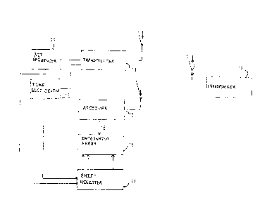
The design in Fig. 1 consists of a transmitter unit 11, an
identification chip 12 which could for example be a passive SAW
transponder, and a receiver unit 13 which is connected to an array 16
of integrator sections. A bit sequencer 14 creates a random bit
sequence which is fed to the transmitter unit 11 and a shift register
17 connected to the integrator array 16. A time slot device 15 forms
a signal with time boundaries which is fed to the transmitter unit 11
and the shift register 17.
The transmitter unit 11 transmits a phase-modulated pulse train
which is received and reflected by the coded transponder 12, so that
the reflected signal consists of a series of pulse trains and spaces
where there are no pulse trains, which together form an identity that
equates to the transponder code, which also consists of
_ 4 _ l 337829
phase-modulated pulse trains. The required signal is picked up by the
receiver 13 which then demodulates it and sends it to an integrator
array 16. This is controlled by the above-mentioned bit sequence from
device 14 together with the time slot from device 15.
Fig. 2 gives a more detailed presentation of the transmitter
unit. This consists of an oscillator 21 which provides a fixed
frequency signal. At phase-modulator 22, this signal is
phase-modulated by a random bit sequence from device 14. Once
modulated, the signal is divided up into pulse trains by means of a
gate device 23, controlled by the time slots from device 15. The
pulse trains are then amplified by an amplifier 24 prior to
transmission.
Fig. 3 shows a more detailed presentation of the receiver and
decoder unit. The signal is demodulated in a receiver 13 into a
time-coded and phase-coded signal 31a, superimposed upon unwanted
noise. In this example of the invention the signal 31a enters a
switch 36a which leads the signal 31a into an integrator section 37.
This integrator section 37 can, for example, be an RC filter with a
high time constant compared to the individual signal cycles (e.g.,
20 10,000 times greater).
The bit sequence from device 14 and the time slot signal from
device 15 form the input to an AND-gate 32a, where the output goes to
a shift register 33a, which then receives exactly the same bit
sequence as that used in the transmitter to form the phase-modulated
pulse train. This bit sequence is then clocked along the shift
register 33a by means of an external clock signal (not illustrated on
the figure). It is possible to obtain a signal from different
positions on the shift register 33a, i.e., after certain intervals of
time after the signal has been fed into the shift register 33a. When
the time interval which equates the time delay for the first bit on
the transponder 12 has elapsed, the signal is removed from the shift
register and used to control the switch 36a that opens or closes the
path for the demodulated signal 31a from the receiver 13 to the
integrator section 37.
The signal 31a can be inverted by means of an inverter 34 to a
signal 31b, which is also fed into the integrator section 37. This is
done by feeding the random bit sequence 14 through an inverter 35 to
- 5 - 1 337829
another shift register 33b and removing it at an equivalent position
to the first shift register 33a and controlling the switch 36b so that
it opens or closes the path for the inverted signal 31b to the
integrator section 37. Both switches 36a and 36b can be controlled
for instance so that a logical "1" in bit sequence 14 opens the switch
for the non-inverted signal 31a from the receiver, and the switch for
the inverted signal 31b closes; if a logical "0" occurs in the bit
sequence 14, the opposite will occur.
In the time interval where pulse trains are not formed from the
transmitter 13 because the signal from device 15 has a logical value
of "0", the AND-gates 32a and 32b will always have a logical "0" in
their output, this ensures that both switches 36a and 36b will be open
to hinder unwanted noise from entering the integrator section.
The integrator array 16 is formed from a number of integrator
sections 37, which typically equate the number of bits or the multiple
of the number of bits in the reflector device 12. The individual
integrator sections 37 can be read whenever the required number of
pulse trains have been processed. This reading can be done
asynchronically without any attention having to be paid to anything
that has happened previously.
Fig. 4 shows a chronological presentation of how two pulse trains
are transmitted from the transmitter 11 and are reflected from the
transponder 12, in an example where the transponder 12 has a
resolution of four bits. Here the transponder 12 is coded with the
bit sequence 1101.
The first pulse train 41a is a phase modulated signal which is
modulated by the first part of a random bit sequence from device 14,
with a length determined by the time slot formed by device 15. The
first pulse train 41a is received by the transponder 12 and reflected
where it is coded to logical "1". As the transponder in this example
has the code 1101, the reflected signal will form a pattern as shown
in 41b where bit 1, bit 2 and bit 4 reflect a pulse train, whilst bit
3, which has the logical value of "0", will not reflect any signal.
The reflecting pulse trains 41b can and will overlap each other in the
various bit positions without having any negative consequences on the
result.
.~
y
- 6 - 1 337829
Once the last reflected pulse train is received, the second pulse
train will be transmitted. This pulse train is phase modulated by
another part of a random bit series, different from that in the first
pulse train, from device 14, with a certain length of time decided by
the time slot in device 15. This second pulse train 42a is then
reflected from the transponder 12 as in the first case, thus forming a
row of reflected pulse trains 42b.
A large number of pulse trains, equivalent to pulse trains 41a
and 42a, all phase modulated in different ways, can be transmitted,
reflected, and led into the integrator array 16 so that the required
signal is averaged and unwanted signals that are random and
asynchronous will be greatly reduced.