Note : Les descriptions sont présentées dans la langue officielle dans laquelle elles ont été soumises.
- ~J-7170
-- 1 --
1 3382 1 8
ECHO CANCELLER
BACKGROUND OF THE INVENTION
1. Field of the Invention
The present invention relates to an echo canceller
used, for example, for a two-wire full-duplex data modem
etc-
In a full-duplex communication system using
the above-mentioned two-wire full-duplex data modem, a
hybrid circuit is adopted for the two wire-four wire
conversion in the data modem and exchange. At the
portion where this hybrid circuit is provided, as
mentioned later, a near-end echo and far end echo return
to the transmission side modem and interfere with normal
communication. An echo canceller is used to eliminate
this interference with communication.
2. Description of the Related Art
One of the technical problems in conventional
echo cancellers has been the frequency offset, explained
in detail later. This is a problem unique to frequency
division multiplex (FDM) type communication systems. If
the echo is cancelled with consideration given to this
frequency offset too, a high quality of echo cancella-
tion can be realized. Therefore; in the past, a
frequency-offset correction circuit has been built into
the echo cancellers.
However, the echo cancellers in the prior art
cannot correct the frequency offset for all far end echo
characteristics. From this viewpoint, there is a first
problem in that an echo canceller with a sufficiently
good quality cannot be realized.
Further an echo canceller must process two
echoes, the near-end echo and far-end echo, separately,
but in actuality since the two echoes return to the
transmission side modem simultaneousIy with the low
level far end echo buried in the high level near end
echo, there is a second problem that the two are
~L
- 2 - 1338218
-
difficult to distinguish. This second problem makes the
resolution of the above mentioned first problem
increasingly difficult. The reason for this is that the
above-mentioned first problem is caused due to only the
far-end echo and has nothing at all to do with the
near-end echo.
SUMMARY OF THE INVENTION
Therefore, the present invention has as its first
object the provision of an echo canceller which can
correct the frequency offset for the far-end echo
characteristics and
has as its second object the provision of an
echo canceller which can distinguish the far-end echo
characteristics from the near-end echo characteristics.
To achieve the above-mentioned objects, the present
invention is first constituted so as to detect the level
of the echo in a received signal, normalize the phase
error between the expected echo and the actual echo
using the detected echo level, and estimate the offset
frequency to be collected using the normalized phase
error and
is second constituted so as to start
cancellation of the near-end echo during a training term
for cancellation of the near-end écho and far-end echo
and to start the cancellation of the far-end echo after
there are no longer any variations in the level of the
near-end echo.
BRIEF DESCRIPTION OF THE DRAWINGS
The above object and features of the present
invention will be more apparent from the foIlowing
description of the preferred embodiments with reference
to the accompanying drawings, wherein:
Fig. 1 is a block diagram of a two-wire full duplex
communication system;
Fig. 2 is a waveform diagram showing the impulse
response of an echo;
Fig. 3 is a block diagram of an example of the
~ 3 ~ l 33821 8
constitution of a data modem provided with a
conventional type of echo canceller;
Fig. 4 is a block diagram of an example of the
constitution of a conventional frequency-offset
correction circuit;
Fig. 5 is a block diagram of the principle of a
first embodiment according to the present invention;
Fig. 6 is a block diagram of details of an echo
canceller of the first embodiment according to the
lQ present invention;
Fig. 7 is a view showing the concrete constitution
of an offset frequency estimation circuit 82;
Fig. 8 is a block diagram of another embodiment of
an echo canceller based on the first embodiment of the
present invention;
Fig. 9 is a block diagram of the principle of a
second embodiment according to the present invention;
Fig. 10 is a block diagram showing in detail a
starting means 140 of Fig. 9;
Fig. 11 is a circuit diagram of details of an echo
canceller of the second embodiment according to the
present invention;
Figs. 12A, 12B, and 12C are signal waveform
diagrams of various portions of the training starting
means for explaining the operation of the circuit of
Fig. 11;
Fig. 13 is a block diagram of the principle of a
third embodiment according to the present invention;
Fig. 14 is a circuit diagram showing the third
embodiment wherein the second embodiment according to
the present invention is incorporated into the echo
canceller of Fig. 6;
Fig. 15 is a circuit diagram for explaining the
gain switch generally used for echo cancellers;
Fig. 16 is a view showing the circuit constitution
when the starting means of the second embodiment is
introduced into an echo canceller including a gain
1 3382 1 8
switch; and
Fig. 17 is a view showing the constitution when the
third embodiment is introduced into an echo canceller
including a gain switch.
DESCRIPTION OF THE PREFERRED EMBODIMENTS
Before describing the embodiments of the present
invention, the related art and the disadvantages therein
will be described with reference to the related figures.
An example of the constitution of a full-duplex
communication system using a two-wire circuit is shown
in Fig. 1. In the figure, the own side data modem 10
includes a modulation circuit (MOD) 11, a hybrid circuit
(HYB) 12, a balancing network (BN) 13, and a
demodulation circuit (DEM) 14 and is accommodated in an
own side exchange through a two-wire subscriber line 15.
The exchange 20 is provided with a hybrid circuit 22 and
a balancing network (BN) 23 and is connected to the
other side exchange 30 through a four-wire transmission
line 24 by the hybrid circuit 22. The other side
exchange 30 is provided with a hybrid circuit (HYB) 32
and a balancing network (BN) 33 and houses the other
side data modem 40 through a two-wire subscriber
line 34. The data modem 40 includes a modulation
circuit (MOD) 41, a hybrid circuit (HYB) 42, a balancing
network (BN) 43, and a demodulation circuit (DEM) 44.
Note that illustration is made of a system using a V.32
modem.
In the communication system, use is made of the
hybrid circuits 12, 22, 32, and 42 for two-wire to four
wire conversion in the data modem and exchange, but if
the impedances of the subscriber lines 15 and 34 and
balancing networks 13, 23, 33, and 43 connected to these
hybrid circuits are not balanced, an echo is caused due
to the leakage of the transmitted signal. As a result,
the transmitted signal sent from the own side modem 10
becomes an echo and returns to the own side modem to
interfere with normal communication.
_ _ 5 _ 1338218
Echoes include, depending on the position of
generation, near-end echoes which are caused by the
leakage of the transmitted signal sent from the modem 10
to the receiver side by the hybrid circuit 12 in the
modem 10 and far-end echoes which are caused by the
leakage of the transmitted signal which reaches the
far-end other side exchange 30 to the opposite side
circuit by the hybrid circuit 32. For full-duplex
communication free from data error in the modem 10, both
of these far-end and near-end echoes have to be
sufficiently suppressed.
An example of the impulse response of near end and
far-end echoes is shown in Fig. 2. In the figure, the
horizontal axis shows the amount of delay from the
transmission of the transmitted signal to the generation
of echo, while the vertical axis shows the amplitude
level of the echo. As shown in the figure, the near-end
echo is comparatively large in level and the amount of
delay is small. On the other hand, the far-end echo
passes through the transmission line 24, so the amount
of delay is great, for example, in the case of a one-hop
satellite transmission path, there is a delay amount of
about 600 msec, and the level is small. Further, the
far-end echo sometimes has a frequency offset.
An echo canceller is known as a means for
suppressing echoes. An echo canceller estimates the
same echo (expected echo) as the resounding echo and
subtracts this from the received signal so as to
suppress the echo. An example of the conventional
constitution of a full-duplex modem provided with such
an echo canceller is shown in Fig. 3.
In Fig. 3, the transmission data is modulated by a
modulation circuit (MOD) 53 through a scrambler 51 and a
data symbol generating circuit 52, then is transmitted
to a two-wire subscriber line lS through a hybrid
circuit (HYB) 12. Further, the reception signal
received from the subscriber line 15 is input to tne
- - 6 - 1338218
demodulation circuit (DEM) 77 through an analog/digital
conversion circuit (A/D) 56 and subtraction circuits 72
and 77 for demodulation, then used as received data
through the automatic equalizing circuit (EQL) 58, code
decision circuit 59, and descrambler 60.
The echo canceller unit includes a near-end echo
canceller 70 for the near-end echo and a far-end echo
canceller 74 for the far-end echo. Before the far-end
echo canceller 74 is placed a bulk delay circuit 73 for
compensating for the transmission delay of the far-end
echo and after it is placed a frequency-offset
correction circuit 75 for correcting the frequency
offset.
The near-end echo canceller 70 generates a signal
the same as the near-end echo based on the transmission
signal, applies the same modulation to this as with the
modulation circuit 53 by the modulation circuit 71, then
subtracts this from the received signal by the
subtraction circuit 72 so as to cancel the near-end echo
in the received signal. Further, the far-end echo
canceller 74 delays the transmission signal by the
amount of delay of the far-end echo by the bulk delay
circuit 73, then generates the same signal as the
far-end echo based on this transmission signal, performs
a frequency offset on this signal by the frequency
offset correction circuit 75, then applies the same
modulation as the modulation circuit 53, and subtracts
the result from the received signal by the subtraction
circuit 77 to cancel the far-end echo in the received
3n signal. The tap coefficients of the near-end echo
canceller 70 and the far-end echo canceller 74 are
subjected to adaptive control based on the error signal
e of the output of the subtraction circuit 77.
The frequency-offset correction circuit 75 corrects
the frequency offset occurring due to the deviation of
the modulation frequency and demodulation frequency for
the frequency division multiplex in an exchange and is
-~ - 7 - l 33821 8
required only for the far-end echo going through the
opposite side exchange.
An example of the constitution of a conventional
frequency-offset correction circuit 75 is shown in
Fig. 4. As illustrated, this includes a phase shift
circuit 83 which rotates an output signal ~n from the
far-end echo canceller 74 by a phase rotation amount ~n
and generates an expected far-end echo signal Yn,, a
phase error extracting circuit 81 which extracts a phase
error ~e between the expected far-end error signal Yn,
and an error signal en, and an offset frequency
estimation circuit 82 which estimates the offset
frequency based on the phase error ~e and outputs a
phase rotation amount '~n so as to make the phase error
~e zero.
This frequency offset correction circuit 75
extracts the phase error ~e using the expected far
end echo Yn, obtained by correction of the frequency
offset with respect to the output signal Yn of the
far-end echo canceller 74, the received signal Yn,
or the error signal en obtained by subtraction of
the expected far-end echo Yn, from the received
signal Yn, corrects the estimated offset frequency
by this phase error ~e I and uses the result as the
correction value for the next sample Yn+l. The above
operation is repeated with every sampling, whereby
adaptive correction of the frequency offset is
performed.
That is, the output signal Yn of the far-end
3~ echo canceller 74 is rotated in phase by exactly
a phase rotation amount ~n from the offset frequency
estimation circuit 82 by the phase shift circuit 83
and the expected far-end echo signal Yn, is produced.
The expected far-end echo Yn, is subtracted from the
received signal rn including the far-end echo Yn,
with a frequency offset by a subtraction circuit 77,
whereby the far-end echo Yn, is cancelled.
_ - 8 ~ l 338 2l 8
The phase error extraction circuit 81 extracts the
phase error ~e between the actual far-end echo Yn, and
the expected far-end echo Yn, from the error signal en
with the expected far-end echo Yn,, and the offset
frequency estimation circuit 82 performs estimation of
the correct offset frequency based on the phase error ~e
and decides the phase rotation amount ~n+1 with respect
to the next sample Yn+1-
An explanation of a first embodiment of the present
invention will be given below.
In general, the size of the far-end echo Yn, in the
received signal rn differs in value for each line to
which the modem is connected, it is known. This is
because the transmission loss differs with each line.
On the other hand, the size of the phase error ~e
which is extracted by the phase error extraction
circuit 81 in the frequency offset correction circuit 75
depends on the size of the far-end echo Yn, in the
received signal rn (proportional to the far-end echo
power or the far-end echo amplitude) and therefore the
estimated offset value of the offset frequency
estimation circuit 82 is also affected by the level of
the far-end echo Yn, . As a result, the characteristics
of the frequency offset correction circuit 75 are
influenced by the connected line, i.e., the size of the
far-end echo Yn, in the received signal. For example,
when the level of the far-end echo Yn, is small, correct
frequency offset correction is not possible, the
following speed becomes slower, or other problems arise.
Therefore, the first object of the present
invention is to make possible stable frequency offset
correction of far-end echoes which is not dependent on
the variations of level of the far-end echoes.
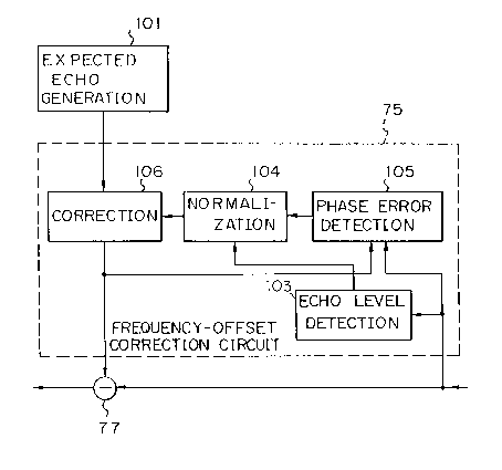
Figure 5 is a block diagram of the principle of a
first embodiment according to the present invention.
The echo canceller according to the first
embodiment of the present invention is provided with an
- 9
1 3382 1 8
expected error generation circuit 101 which generates an
expected error of a transmission signal and a frequency
offset correction circuit 75. The frequency offset
correction circuit 75 is provided with a phase error
detection circuit 105 whick detects the phase error
between the echo in the received signal and the expected
echo of the expected echo generation circuit 101, a
correction circuit 106 which corrects the frequency
offset of the expected echo by the frequency offset
estimated based on the phase error, an echo level
detecting circuit 103 which detects the size of the echo
in the received signal, and a normalizing circuit 104
which normalizes the phase error by the echo level
detected by the echo level detection circuit 103. The
echo in the received signal is suppressed by use of the
expected echo after correction of the offset by the
frequency offset correction circuit 75.
The phase error detected by tbe phase error
detection circuit 105 differs in size along with
variations in the echo level in the received signal.
This variation interferes with normal estimation of the
offset frequency. Therefore, use is made of the echo
level detected by the echo level detection circuit 103,
the phase error is normalized by the normalizing
circuit 104, and the offset frequency is estimated based
on the normalized phase error. The offset frequency
estimated in this way is used for correction of the
frequency offset of the expected echo, then the expected
echo is used for cancellation of the echo in the
received signal.
Figure 6 is a block diagram of details of an echo
canceller of the first embodiment according to the
present invention. In the figure, the transmission
circuit includes a scrambler 51, a data symbol
generating circuit 52, a waveform shaping filter 55, a
modulation circuit 53, a D/A conversion circuit 54, and
a hybrid circuit 12. The reception circuit includes
- 10 _ 1338218
hybrid circuit 12, an A/D conversion circuit 56,
subtraction circuits 72 and 77, a demodulation
cilcuit 57, an automatic equalizing circuit 58, a code
decision circuit 59, and a descrambler 60.
The complex transmission signal an output from the
data symbol generating circuit 52 in the transmission
circuit is input through the modulation circuit 61 to
the near-end echo canceller 70 and along with this is
input through the bulk delay circuit 73 which corrects
the delay of the far-end echo to the far-end echo
canceller 74. Note that the n in the suffix means the
sampling number. Further, the underbar indicates a
vector quantity. The output signal of the far-end echo
canceller 70 is input to the subtraction circuit 72
where it is subtracted from the received signal. The
result is used for cancellation of the near-end echo in
the received signal.
On the other hand, the output signal Yn of the
far-end echo canceller 74 is input through the frequency
offset correction circuit 75 to the subtraction
circuit 77, where it is subtracted from the received
signal, whereby the far-end echo Yn, in the received
signal rn is cancelled. Note that the modulation
circuit 61 performs the same modulation as the
modulation circuit 53 on the input signal.
The near-end echo canceller 70, far-end echo
canceller 74, and frequency offset correction circuit 75
are constituted so as to be adaptively controlled by the
error signal en output from the subtraction circuit 77.
The frequency offset correction circuit 75 is
provided with the abore-mentioned phase error extraction
circuit 115, offset frequency estimation circuit 82, and
phase shift circuit 83 and also a far-end echo power
measuring circuit 113 which measures the signal power y2
of the far-end echo Yn, in the received signal rn and a
divider 114 which forms a normalizing circuit 104 which
normalizes the phase error ~e from a multiplier 115
- 11 - 1 33821 8
which forms a phase error extraction circuit 105 using a
far-end echo power Y measured by the far-end echo power
measurement circuit 113. The offset frequency
estimation circuit 82 is constituted so as to perform
estimation of the offset frequency using the phase error
~e' normalized by the normalizing circuit 114.
The operation of the apparatus of Fig. 6 will be
explained below:
The echo canceller is constituted by a near-end
echo canceller 70 and a far-end echo canceller 74. The
echo cancellers 70 and 74 receive as input the complex
symbol an, obtained by rotating the complex transmission
signal a = Xn + jy of the baseband at the carrier
-n n
frequency WC by the modulation circuit 61 . That is,
a , - an.exp (-jwc.nT) (1)
Here, WC is the carrier frequency and l/T is the
modulation speed. Note that the far-end echo canceller
74 receives as input a signal delayed by the bulk delay
circuit 73 by exactly the amount of delay of the far-end
echo Yn, measured in advance.
If the input data vector sequence AnT is
A (-n'' -n-l' ' -n-2' -T ' -n-N+l) (2)
and the tap coefficient vector H is
T ~ ~ ~ -n A
H (hn,0 ' hn,l ' hn,2 ' hn,N-1) (3)
the far-end echo canceller 74 outputs the output
vector yn calculated by the following equation (4).
Note that here N is a tap coefficient and the hat
"A" shows the estimated value.
Yn = An Hn ( ~ Yn ~ i Yn
The output signal Yn of the far-end echo
canceller 74 is next input to the frequency offset
correction circuit 75 and is rotated by exactly the
phase rotation amount ~n of the offset frequency
estimation circuit 82 by the phase shift circuit 83 of
the frequency offset correction circuit 75. By taking
an imaginary part thereof,
the expected far-end echo Yn, is produced. That is,
- - - 12 -
1 3382 1 8
Yn = Im [YneXPti~n)]
= Yn sin~n + yn*cos~n (5)
Note that the tap coefficient vector HnT of the
far-end echo canceller 74 is adaptively controlled based
on the error signal en
en rn Yn' (6)
Here, rn is the received signal after cancellation of
the near-end echo.
On the other hand, the phase error extraction
multiplier 115 receives as input the expected far-end
echo Yn, and the received signal rn . By finding the
product of the same, the phase error ~n of the far-end
echo Yn, , that is, the phase deviation between the
actual far-end echo Yn, and the expected far-end echo
Yn~.
That is,
~e = Yn'~rn
y~, (Yn~ + ~n)
= (Yn sin~n + Yn*CS~n)
x (Yn CS~n ~ yn*sin~n + ~n)
Here, ~n is signal components other than the
far-end echo, such as the noise, residual near-end
echo, far-end data signal.
In the above equation (7), the actual far-end
echo Yn, is expressed by
Yn~ Yn cS~n ~ Yn* sin~
Here, Yn is the output of the echo path not
having a frequency offset, Yn* is the Hilbert
Yn, n 0 0
3~ is the offset angular frequency. That is, the actual
far-end echo Yn, is considered the output Yn f
the echo path not having a frequency offset subjected
to single side band modulation at the offset fequency
o
Here, if the estimation of the transmission
characteristics of the echo path by the echo canceller
is assumed to be done well, the approximation Of Yn ~
- 13 - 13382~8
Yn ~ Yn* ~ Yn* stands, so equation (7) can be
approximated as follows:
$e = y2 cos~n sin~n
- y* cos~n sin~n
+ YnYn* (cosr~n coS~Sn ~ sin~n sin~n)
+ (yn sin~n + Yn* CS~n) ~n (8)
Here, the estimated value E [~e] of the phase error
~e is found as follows from the fact that YnYn* are
noncorrelative signals.
E [~e] = Y s~in (~n ~n)
~ Y (~n ~ ~n) + Y R (9)
Here, Y = E [y ] = E [y* ]
R = E [~ ]
As will be understood from equation (9), the phase
error ~e is proportional to the phase error (~n ~ ~n)
between the expected far-end echo yn' and the actual
far-end echo Yn, and further is proportional to the far
end power Y (Y.R time average is 0). Therefore, when
the level of the far-end echo is small, the phase error
2~ ~e becomes small, so there is a possibility of the
frequency offset estimation not going well.
Therefore, the far-end echo power y2 is measured
from the received signal rn in advance by the far-end
echo power measurement circuit 113 and the phase error
~e from the phase error extraction multiplier 115 is
divided by the far-end echo power y2 and normalized,
whereby a phase error ~e' not dependent on the far-end
echo level is obtained. The offset frequency estimation
circuit 82 estimates the offset frequency of the far-end
3~ echo based on this phase error ~e' and decides on the
phase rotation amount '~n+l for the next output sample
Yn+l of the echo canceller.
Note that the measurement of the far-end echo power
Y by the far-end echo power measurement circuit 113 is
performed in the training term performed before the data
communication and that the measurement value is held
continuously during the foIlowing communication term.
- 14 - l 33821 8
As opposed to this, the offset correction performed by
the phase error extraction circuit 115, offset frequency
estimation circuit 82, and phase shift circuit 83 is
performed with every sample while communication is
underway.
Figure 7 is a view showing the concrete constitu-
tion of an offset frequency estimation circuit 82. In
the figure, reference numeral 116 is an integration
circuit which includes a delay circuit T, a tap setter C
which multiplies the output by a suitable control
coefficient, and an adder ~ . After this there is a
vector integration circuit 117 which has a multi-
plier ~ . A multiplier 118 forms a complex multiplier.
Note that reference numeral 119 is a feedback path which
stabilizes the operation of the offset frequency
estimation circuit 82.
In realizing the first embodiment of the present
invention, various modifications are possibIe. In the
above-mentloned specific example (Fig. 6), use is made
of the power y2 of the far-end echo for normalizing the
phase error from the phase error extraction circuit
(115), but the present invention is not limited to this
and use may be made of the amplitude Y of the far-end
echo for normalizing the phase error ~e.
That is, Fig. 8 is a block diagram of an embodiment
in the case of normalizing the phase error using this
far-end echo amplitude Y, wherein there is shown a
far-end echo canceller 74 and a frequency offset
correction circuit 75.
In this embodiment, the phase shift circuit is
constituted by multiplication circuits 131 and 132 which
respectively multiply the Yn ~ Yn* of the Yn = Yn + iYn
output signal of the far-end echo canceller 74 and the
rotational phases sin~n, cos~n from the offset frequency
estimation circuit 92 and an addition circuit 133 which
adds the outputs of the multiplication circuits 131
and 132. The phase error extraction circuit is
13382~8
constituted by the sign function circuits 134 and 135 to
which are input the output signals of the multiplication
circuits 131 and 132, multiplication circuits 136
and 137 which multiply the received signals rn with the
output signals from the sign function circuits 134
and 135, and an addition circuit 138 which adds the
output signals from the multiplication circuits 136
and 137. Further, the far-end echo amplitude
measurement circuit 123 is a circuit for measuring the
amplitude ¦Y¦ of the far-end echo Yn, in the received
signal rn . The already mentioned normalization
circuit 104 is formed by the multiplier 124 for
normalizing the phase error ~e by dividing it by the
far-end echo amplitude Y.
The operation of the example of Fig. 8 will be
explained below. In this example, the phase error ~e is
found by the following equation (10):
~e = (sign [Yn sin~n]
+ sign [Yn* cos~n]) rn
= (sign [Yn sin~n] + sign [Yn* cos~n])
(Yn cS~n ~ Yn* sin~n)
= sign [Yn sin~n] Yn cos~n
- sign [Yn* cos~n] Yn* sin~n
+ sign [Yn* cos~n] Yn cos~n
- sign [Yn sin~n] Yn* sin~n (10)
where,
sign [A sin 0] A = ¦A¦ sign [sin 0]
sign [A cos a ] A = ¦A¦ sign [cos o]
Further, if y and y* are approximated as y and y*,
~n = IYnl sign [sin~n] cos~n
- IYn*l sign [cos~n] sin~n
+ sign [Yn* cos~n] x Yn cos~n
- sign [Yn sin~n] Yn* sin~n (11)
The third term and fourth term at the right side of
equation (11) are noncorrelative signals, so the
expected value E [~e] of the phase error ~e becomes as
follows:
- 16 - 1 33821 8
E [~e] ~ YSin (~n ~n)
~ ( n ~n) (12)
where, Y = E [IYnl] = E [¦Yn*¦]
As will be understood from equation (12), the phase
error ~e found from the equation (10) is proportional to
the average amplitude of the far-end echo. Therefore,
if the average amplitude is measured by the far-end echo
amplitude measurement circuit 123 and the phase error ~e
is divided by the amplitude Y by the divider 124, it is
possible to obtain the normalized phase error ~e'
Based on this phase error ~e'' the offset frequency is
estimated by the offset frequency estimation circuit 92.
As explained above, according to the first
embodiment of the present invention, it is possible to
correct the frequency offset of a far-end echo in a
stable manner not dependent on variations of the level
of the far-end echo.
Note that to speed understanding of the invention,
the afore-mentioned constituent elements are expressed
as independent functional blocks, but in actuality they
are realized in a program by software processing of a
processor and the echo canceller is constituted by a
microprocessor consisting of several chips. The same
applies to the next explained second embodiment.
Below, an explanation will be made of the second
embodiment. As mentioned before, the near-end echo
canceller 70 and the far-end echo canceller 74 are
refreshed using the same error signal en (that is, the
error signal e output from the subtraction circuit 77 in
Fig. 3). This error signal en is as follows in the
conventional apparatus of Fig. 3:
n Yl,n Y2~n
Yl~n Y2~n ~ n (13)
Here, Yl is the near-end echo, Y2 is the far-end
echo, Y1 is the output of the modulation circuit 71, Y2
is the outpu~ of the demodulation circuit 76, and ~ is
noise or another signal which cannot be cancelled.
_- 17 - 1 33821 8
Therefore, it is possible to find from the
following equation the tap coefficient vector hl of the
near-end echo canceller 70 and the tap coefficient
vector h2 of the far-end echo canceller 74. Note that
here an is the input data vector of the near-end echo
canceller 70 and that bn is the input data vector of the
far-end echo canceller 74.
hl,n+l hl,n (Ylln Yl,n) an
~ A+ ~ (Y2,n ~ Y2~n + ~n) an (14)
k2,n+1 h2,n + (Y2,n Y2,n) bn
(Yl,n Yl~n ~n) bn (15)
In the conventional apparatus, when finding the tap
coefficient of the echo canceller based on the
above-mentioned equations (14) and (15), the third term
on the right side in the equations is a noncorrelative
signal, so interferes with the estimation of the correct
coefficient vector. In particular, the near-end echo is
larger than the far-end echo by 40 to 50 dB in some
cases, so in the training term before the communica-
2~ tions, the far-end echo canceller will operate unstably
and not be able perform correct adaptive operation in
the period until the near-end echo canceller is
sufficiently restrained and the residual near-end echo
level becomes sufficiently small.- In some cases, during
that period, normal training cannot be performed.
Therefore, in the training, consideration may be
given to the method of first training just the near-end
echo canceller and after the residual echo of the
nearend echo is suppressed to about the same level as
the far-end echo, starting to train the far-end echo
canceller and the attendant frequency offset correction
circuit, thus preventing the far-end echo canceller from
operating unstably. In this case, the level of the
far-end echo is very different with each connection
line, so it is necessary to measure the far-end echo
level for the training with each communication.
However, it is in general difficult to extract just the
- 18 - 1338218
-
far-end echo from the echo signal and measure its level
since the frequency band region is the same as the
near-end echo.
Therefore, in the second embodiment of the present
invention, a circuit which can accurately detect the
timing at which the near-end echo is sufficiently
suppressed to about the level of the far-end echo
without the direct measurement of the level of the
far-end echo during training is realized by a simple
construction and thereby the training of the far-end
echo canceller is started at a precise timing to
eliminate instability in the training operation of the
far-end echo canceller. This is very beneficial to the
previously mentioned first embodiment wherein the
assumption is the extraction of just the far-end echo.
Figure 9 is a block diagram of the principle of the
second embodiment according-to the present invention.
The echo canceller according to the second embodiment of
the present invention is provided with a starting
means 140 which finds the rate of change of the error
signal ~ between the output signal of the near-end echo
canceller 70 and tke received signal R and starts the
training of the far-end echo canceller when the rate of
change is sufficiently small. The training of the
near-end and far-end echo cancellers 70 and 74 is
designed so that during the training, the training of
only the near-end echo canceller 70 is first started and
that the training of the far-end echo canceller 74 is
started by the starting signal S from the starting
means 140. In the figure, note, reference numerals 72
and 77 are subtraction circuits.
Next, an explanation will be given of the operation
of the echo canceller of Fig. 9. In the training
preceding the communications, first, training of only
the near-end echo canceller 70 is performed. This
enables adaptive determination of the tap coefficient of
the near-end echo canceller 70. The near-end echo in
- 19 - 1338218
the received signal R is gradually suppressed by the
output signal of the near-end echo canceller 70, and the
error signal ~ which is the difference of the received
signal R and the output signal of the near-end echo
canceller 70, becomes gradually smaller. Finally, it is
restrained to a certain level consisting of a noise
component, far-end echo, or residual echo component
which cannot be eliminated. Therefore, if the rate of
change of the error signal ~ is measured, it is possible
to detect that the error signal has been restrained to a
certain level by the fact of the rate of change becoming
sufficiently small. If the training of the far-end echo
canceller 74 is started at this timing, the residual
level of the near end echo becomes about the same as the
far-end echo and training is possible without
instability of operation of the far-end echo canceller.
Figure 10 is a block diagram showing in detail the
starting means 140 of Fig. 9. The means includes an
error signal level detecting means 141 which detects the
level of the error signal ~, a differentiating means 142
which extracts the change in the error signal level
detected, and a differential coefficient detecting
means 143 which detects the differential coefficient of
the output of the said differentiating means. The
means 143 outputs a starting signal S when the
differential coefficient becomes almost zero.
Figure 11 is a circuit diagram of details of an
echo canceller of the second embodiment according to the
present invention. In the figure, constituent elements
the same as in Fig. 6 are given the same reference
numerals or symbols.
The near-end echo canceller 70, the far-end echo
canceller 74, and the frequency offset correction
circuit 75 are constituted so as to be adaptively
controlled by the error signal e output from the
subtraction circuit 77, but the embodiment is set up so
that the far-end echo canceller 74 and the frequency
- 20 - 1 3382 ~ 8
offset correction circuit 75 are begun to be trained
only after receipt of a starting signal S from training
starting means 140 shown by the broken lines in the
figure.
The training starting means 140 includes a
square circuit 150 which squares the error signal ~,
obtained by subtracting the output signal of the
near-end echo canceller 70 from the received signal R
by the subtraction circuit 72, to find the power,
a low pass filter (LPF) 151 which filters the output
signal of the square circuit 150, a differentiating
circuit 152 which differentiates the output signal
of the low pass filter 151, and a differential
coefficient detection means 143 which outputs a
starting signal S to the far-end echo canceller 74 and
frequency offset correction circuit 75 in accordance
with when the output signal of the differentiating
circuit 152 becomes zero or sufficiently small. Note
that, referring to Fig. 10, the constituent element 141
of Fig. 10 is realized by the constituent elements 150
and 151 of Fig. 11, and the constituent element 142 of
Fig. 10 is realized by the constituent element 152 (153,
154, and 155) of Fig. 11.
The differentiating circuit-152 includes a
switch 153 for down-sampling to 1/16 the input signal by
closing for one time with each 16 clock timings, a
delay circuit 154 which delays the input signal by 16
clocks, and a subtraction circuit 155 which generates
the differential of the input signal by taking the
difference of the input signal and the output signal
of the delay circuit 154. Regarding this down sampling
circuit, the differential is obtained by the
differentiating circuit 152 by taking the difference
with the past sample, but usually the sampling frequency
of the output signal of the subtraction circuit 72 is a
high 9600 Hz or 7200 Hz or so, so the differential of
the subtraction circuit 155 sometimes becomes ~oo small.
- 21 - 1338218
Therefore, the down sampling is performed so as to
prevent this.
Below, an explanation will be made of the operation
of the echo canceller of Fig. 11 with reference to
Figs. 12A, 12B, and 12C. Figures 12A, 12B, and 12C are
diagrams of signal waveforms at various portions (12A,
12B, and 12C) of the training starting means 140 in
Fig. 11. In the figure, Fig. 12A shows the restraint
characteristics of the residual echo power in the case
where just the near-end echo canceller is operated
during training and shows the power of the input signal,
i.e., error signal, to the training starting means 140,
that is, the waveform of the output signal of the square
circuit 150. Figure 12B shows the waveform of the
output signal of the low pass filter lSl, and Fig. 12C
shows the waveform of the output signal of the
differentiating circuit 152.
First, training of the echo canceller is performed
before the communication, but at the start of tke
training, only the near-end echo canceller 70 is
trained, i.e., the far end echo canceller 74 and the
frequency offset correction circuit 75 are in an idle
state. The near-end echo canceller 70 is controlled
adaptively in its tap coefficient-by the error signal e
of the output of the subtraction circuit 77. As a
result, the A/D converted received signal R gradually
has the near end echo removed at the output of the
subtraction circuit 72. The residual component of tke
near-end echo, which was the level LN (L: Level, N:
Near-end) at the start of the training as shown by
Fig. 12A, gradually declines along with the restraint of
the near-end circuit 70 and stabilizes at the level LF
(F: Far-end) of either the far-end echo level or noise
level, whichever is greater.
Therefore, the timing at which the training of the
far-end echo canceller 74 is started may be made the
timing tl where the residual echo level becomes LF, so
1 33821 8
- 22 -
by squaring the residual echo signal ~ by the square
circuit 150 to obtain the power value and then smoothing
the result by the low pass filter 151 to obtain the
waveform of Fig. 12B and further by differentiating in
time the result by the differentiating circuit 152 to
obtain the waveform of Fig. 12C, the time tl can be
detected by when the differential output signal of the
differentiating circuit 152 becomes zero or sufficiently
small. This is detected by the differential coefficient
detecting means 143, which generates a starting
signal S, whereby the training of the far-end echo
canceller 74 and the frequency offset correction
circuit 75 is started.
According to the above, it is possible to detect
the optimum starting timing tl of the far-end echo
canceller 74 without prior measurement of the far-end
echo level LF by when the output signal of the
differentiating circuit 152 becomes zero or sufficiently
small.
In the working of the present invention, various
modifications are possible. For example, in the
above-mentioned embodiment, the input signal of the
training starting means 140 was obtained from the
subtraction circuit 72 directly after the removal of the
far end echo, but the present invention is not limited
to this. It is possible to obtain it from the error
signal e from the subtraction circuit 77. Further, in
the training starting means 140, the differential is
found by converting the input signal to the power amount
by the square circuit 150, but of course the
differential may be found by the absolute value of the
input signal.
As explained above, according to the second
embodiment of the present invention, it is possible to
realize, by a simple construction, a circuit which can
accurately detect the timing at which, during training,
the near-end echo is sufficiently suppressed to about
1 3382 1 8
- 23 -
the far-end echo level without direct measurement of the
far-end echo level. By this, it is possible to prevent
instability of the training operation of the far-end
echo canceller by starting the training of the far-end
echo canceller at a precise timing.
The function derived from the above-mentioned
second embodiment can be effectively utilized in the
first embodiment which operates by extracting just the
far-end echo.
Figure 13 is a block diagram of the principle of a
third embodiment according to the present invention,
which constitutes the previously mentioned second
embodiment incorporated into the first embodiment. Note
that all the constituent elements in Fig. 13 have
been previously explained. In Fig. 13, the frequency
offset correction circuit 75 starts operating only when
the starting signal S is output.
Figure 14 is a circuit diagram showing the third
embodiment wherein the second embodiment according to
the present invention is incorporated into the echo
canceller of Fig. 6. All the constituent elements have
already been explained.
For efficient operation of the echo canceller, use
is generally made of a gain switch (SW). When the
starting means 140 is incorporated into the echo
canceller based on the above-mentioned second
embodiment, consideration must be given to cooperation
with the gain switch as well. Below, an explanation
will be given of the reasons why the gain switch is
needed. Further, an explanation will be given of the
modifications which should be made to the gain switch
when incorporating the above-mentioned second
embodiment.
When the echo cancellation algorithm in the echo
canceller is realized by fixed point calculation, it is
desirable in reducing the calculation error that the
level of the received signal input to the subtractor for
1 3382 1 8
- 24 -
subtracting the expected echo be made as large as
possible without overflow of the tap coefficient or
calculation value of the calculation process. This is
because when the received signal, more precisely the
echo level in the received signal, is small, the tap
coefficient of the echo canceller becomes small and the
number of digits of the effective numerals in a word
becomes small, which causes calculation error.
In general, the far-end echo becomes the same level
or lower as the far-end data signal. On the other hand,
when the line attenuation is large, the near-end echo
sometimes becomes larger than the far-end data signal by
30 dB or more.
Therefore, there are times when the output of the
subtractor 72 (Fig. 14), which subtracts the expected
near-end echo from the received signal, becomes
considerably small, but if this is input as is to the
subtractor 77 (Fig. 14), the calculation error of the
far-end echo canceller becomes large. Therefore, a gain
switch is inserted into the output of the subtractor 72
and thus the input of the subtractor 77 is held to a
constant level.
Figure 15 is a circuit diagram for explaining the
gain switch generally used for echo cancellers. The
gain of the gain switch 160 shown in the figure is found
by measuring the level of the far-end data signal before
the training of the echo canceller. Note that since in
this case the input level of the subtractor 77 is
maintained constant at all times, so it is possible to
adaptively change the gain of the gain switch 160, but
in this case it is necessary to change the gain of the
far-end echo canceller as well along with this.
Further, the effect of the echo canceller performing
this adaptive operation is felt and the two become
unstable in some cases, so this is not used too much.
On the other hand, the output of the subtractor 72
includes a large residual far-end echo before the
- 25 - l 3382 1 8
completion of the training, so the level is large.
Therefore, if a gain found from the far-end data signal
is given in advance to the gain switch 160, the output
overflows. For this reason, it is impossible to make
the gain of the gain switch 160 a suitable value until
the completion of the training of the echo canceller and
the calculation error of the far-end echo canceIler
dwing the training becomes large.
The present invention attempts to resolve
this problem of the prior art too and provides a
data modem echo canceller which has a near-end echo
canceller and far-end echo canceller, wherein it is
possible to switch to the most suitable gain for each
line and give the same to the gain switch during the
training and therefore it is possible to reduce the
calculation error during the training in the far-end
echo canceller which performs the fixed decimal point
computation.
As shown in the embodiment of Fig. 16, there is
provided an echo canceller having a first subtractor 72
which subtracts the expected near-end echo from the
received signal, a gain switch 160 which amplifies the
output of the first subtractor 72, and a second
subtractor 77 which subtracts the-extracted far-end echo
from the output of the gain switch 160, which echo
canceller is provided with a starting signal generating
means 140, the gain of the amplifier 160 being made a
predetermined low value during the training period of
the echo canceller and being made a high value when the
starting signal is generated from the starting signal
generating means 140.
When the training starts, the gain of the gain
switch 160 is made l, it is judged when the rate of
reduction of the error signal after subtracting the
expected near-end echo from the received signal becomes
small due to the restraint of the near-end echo
canceller, and subsequent to this the gain of the gain
_ - 26 - l 33821 8
switch is set to a pre-found value, whereby overflow of
the gain switch output is prevented.
Therefore, the square mean value of the signal
after removal of the near-end echo is found, the time
when the differentiating value in time becomes zero or
sufficiently small is detected, and a starting signal S
for switching the gain in the gain switch is generated.
In Fig. 12A, the time tl when the residual echo
became a constant value was the time when the
differential became zero or sufficiently small, as shown
in Fig. 12C, so if the starting signal S is generated at
that point of time, it is possible to switch the gain of
the gain switch at the optimal timing even without
measurement of the level LF
In this case, the level LF is the same as or
smaller than the level of the far-end data signal, so
even if the gain of the gain switch at the point of time
tl determined as mentioned above is switched to a gain
found in advance based on the level of the far-end data
signal, the output of the gain switch will not overflow.
In Fig. 16, the differential coefficient detecting
means 143 detects when the signal of the differential at
the subtractor 155 becomes zero or sufficiently small
and issues a starting signal. The gain switch 160
raises the gain of when this starting signal is
received. In this way, the starting means 140 can judge
the restraint of the near-end echo canceller by the
differential of the output of the subtractor 72 becoming
zero or sufficiently small and generate a starting
signal which switches the gain of the gain switch 160.
The far-end echo canceller 74 is adaptively
controlled by the error signal e at the output of the
subtractor 77. By this, the expected far-end echo Y2 is
subtracted at the subtractor 77 (point c) to remove the
far-end echo, but the gain switch 160 at the input side
of the subtractor 77 has a low gain at the start, so
even when the far-end echo is not sufficiently removed,
1 33821 8
- - 27 -
there is no overflow at the gain switch 160. Further,
when the near-end echo is sufficiently removed at the
output of the subtractor 72, the gain at the gain
switch 160 rises by the starting signal S from the
starting means 140, so it is possible to reduce the
calculation error of the far-end echo at the
subtractor 77. Therefore, with this echo canceller,
even if use is made of a fixed decimal point calculation
circuit, it is possible to reduce the calculation error
of the far-end calculation circuit during the training.
Note that in the circuit of Fig. 16, the waveform
shaping filter 55 is used to prevent the occurrence of
interference between symbols defined by the multivalue
signal output from the data symbol generating
circuit 52.
As mentioned above, it is possible to generate a
signal for switching the gain in the gain switch
inserted between the expected near-end echo subtractor
and expected far-end echo canceller during the training,
so it is possible to reduce the calculation error during
training at the far-end echo canceller which performs
the fixed decimal point computation.
Figure 17 is a view showing the constitution when
the third embodiment is introduced into an echo
canceller including a gain switch. This includes the
constitution of Fig. 13 plus a gain switch 160 which is
controlled by the starting signal S from the starting
means 140.
As explained above, according to the present
3~ invention, an echo canceller is realized which can
correct the frequency offset according to the far-end
echo characteristics.