Note : Les descriptions sont présentées dans la langue officielle dans laquelle elles ont été soumises.
1339553
MATERIAL FOR RESISTOR BODY AND NON-LINEAR RESISTOR MADE THEREOF
BACKGROUND OF THE INVENTION
Field of the Invention
The present invention relates generally to a
non-linear resistor which is suitable for use in a lightning
arrestor, surge absorber and so forth. More particularly, the
invention relates to a material for non-linear resistor which
has excellent electrical and mechanical characteristics.
Description of the Background Art
Non-linear resistors have known electric
characteristics to non-linearly increase current according to
increasing voltage and whereby lower voltage in non-linear
fashion. Such non-linear resistor are known as useful element
for absorbing extraordinarily high voltage. Therefore, the
non-linear resistors have been used in a lightning arrestor,
surge absorber and so forth.
One of typical composition of a material for forming
the non-linear resistor contains zinc oxide as primary
component. The non-linear resistor material is further
composed of relatively small amount of oxides, such as bismuth
trioxide (Bi2O3), cobalt oxide (Co2O3), manganese dioxide (MnO2),
antiminial oxide (Sb2O3) and so forth. The composite material
is prepared by mixing the compositions set forth above and by
crystalizing. The composite material is then shaped into a
desired configuration and fired at a given temperature. Such
non-linear resistor material has a three-dimensional structure
having ZnO crystal (10 ~1 - cm) of 10 ~m surrounded by high
resistance intergranular layer of less than or equal to 0.1 ~m
thick, which intergranular layer contains Bi2O3 as primary
component.
As is well known, the intergranular layer filling up
gaps between ZnO crystals has an electric property or
characteristics to substatially and non-linearly decrease
resistance according to increasing of chanrged voltage. When
composition is held unchanged, voltage/current characteristics
' 1339553
- 2 -
of each unit of crystal-lnsulative intecgranular layer-crystal
is considered to be substantially constant.
As set forth, the non-linear resistors have
considered useful because of excellent electric or non-linear
voltage/current characteristics. However, the conventional
non-linear resistors were not satlsfactory in mechanlcal
characteristics, such as compression strength, bending strength
and so forth because interest was concentrated to electric
characteeistlcs. Because of lack of mechanical strength,
appllcation of the non-llnear reslstor has been llmlted.
SUMMARY OF THE INVENTION
Therefore, it is an object of the present invention
to providè a material for forming a non-llnear reslstor whlch
exhibits not only excellent voltage/c,urrent characteristics but
also excellent mechanical characteristics.
Another object of the invention is to provide a
non-linear resistor which has satisfactory voltage absorbing
ability with sufficiently high mechanical strength.
In order to accompllsh aforementioned and other
objects, an average size of ZnO particles whlch are three
dimenslonally connected and serve as primary component of a
non-linear resistor, is adjusted to be withln a range of 5 ~m
to 10 ~m.
According to the present invention, there is
provided a non-linear resistor which includes a
resistor body formed wi ~
- 3 - 1339~5~
a composite material composed of:
Bi2~3 0.25 to 1.0 mol%;
Sb2O3 0 5 to 2.0 mol~;
C~2~3 0.25 to 1.0 mol%;
MnO2 0.25 to 1.0 mol%;
Cr2O3 0.1 to 1.0 mol%;
NiO2 0.1 to 1.0 mol%;
SiO2 0.25 to 2.0 mol%; and
ZnO remainder for 100 mol%, and
the resistor body including ZnO crystal, average
particle size of which is adjusted within a range of 5 ~m to 10
~m.
According to another aspect of the invention, a
non-linear resistor which includes a resistor body, an
insulating layer formed on the circumference of the resistor
body, electrodes formed on both axial ends of the resistor
body, the resistor body being formed with a composite material
composed of:
Bi2~3 0.25 to 1.0 mol%;
Sb2O3 ~ S to 2.0 mol%;
Co2O3 0.25 to 1.0 mol%;
MnO2 0.25 to 1.0 mol%;
Cr2O3 0.1 to 1.0 mol%;
NiO2 0.1 to 1.0 mol%;
SiO2 0.25 to 2.0 mol%; and
ZnO remainder for 100 mol%, and
the resistor body including ZnO crystal, average
particle size of which is adjusted within a range of 5 ~m to 10
~m.
Preferably, the resistor body is provided a
compression strength approximately and higher than 70 kgf/mm .
Also, the non-linear resistor has energy absorption capacity
ratio approximately or higher than 1.00, and/or ~V/V variation
ratio approximately or lower than 1.0
The preferred average particle size of ZnO crystal is
in a range of 7 ~m to 9 ~m. Further preferably, the non-linear
1339~i53
-- 4 --
resistor is provided a compression strength approximately and
higher than 80 kgf/mm , energy absorption capacity ratio
approximately or higher than 1.10 and/or ~VJV variation ratio
approximately or lower than 0.8.
According to a further aspect of the invention, a
process for producing a non-linear resistor comprising the
steps of:
preparing composite material by mixing the following
components
Bi2~3 0.25 to 1.0 mol%;
Sb2O3 0 5 to 2.0 mol%;
Co2O3 0.25 to 1.0 mol~;
MnO2 0.25 to 1.0 mol%;
Cr2O3 0.1 to 1.0 mol%;
NiO2 0.1 to 1.0 mol%;
SiO2 0.25 to 2.0 mol%; and
ZnO remainder for 100 mol~,
forming the composite material into a desired
configuration to form a shaped body; and
performing firing of the shaped body at a controlled
firing temperature, which firing temperature is adjusted to
adjust average particle size of ZnO crystal growing during the
firing process within a range of 5 ~m to 10 ~m.
Preferably, the process further comprises the step performed in
advance of firing step for pre-firing the shaped body at a
temperature lower than the firing temperature. The pre-firing
step is followed by a step of applying insulative material on
the circumference of the shaped body.
On the other hand, the firing process may be followed by
a step of applying insulative mater~al on the circumference of
the shaped body. The insulative material applying step is
further followed by a step of firing the insulative material to
form an insulation layer on the circumference of the shaped
resistor body and of heat treatment of the shaped resistor~5 body.
According to a still further aspect of the invention,
133g553
a process for producing a non-linear resistor comprising the
steps of:
preparing composite material by mixing the
following components
Bi2o3 0.25 to 1.0 mol%;
Sb2O3 0.5 to 2.0 mol%;
C~2~3 0.25 to 1.0 mol%;
MnO2 0.25 to 1.0 mol%;
Cr2O3 0.1 to 1.0 mol%;
Nio2 0.1 to 1.0 mol%;
sio2 0.25 to 2.0 mol%; and
Zno reminder for 100 mol%,
forming the composite material into a desired
configuration to form a shaped body;
performing firing of the shaped body at a
controlled firing temperature, which firing temperature is
adjusted at approximately or lower than 1150~C, and
Controlling, during the firing process, the
particle size of ZnO particles to be 5 ~m to 10 ~m in
average.
Preferably, the firing temperature is at
approximately or lower than 1100~C and at approximately or
higher than 1050 ~C.
BRIEF DESCRIPTION OF THE DRAWINGS
The present invention will be understood from the
detailed description of the invention in terms of examples,
which will be discussed hereafter with reference to the
accompanying drawings, and which, however, should not be
taken to limit the invention to the specific embodiments but
for explanation and understanding only.
In the drawings:
1339~53
- 5a -
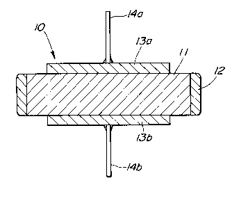
Fig. 1 is a cross-section of the preferred
embodiment of a non-linear resistor according to the present
invention, which non-linear resistor is composed of the
preferred composition and preferred structure of material;
Fig. 2 is an enlarged section showing general
structure of the non-linear resistor of Fig. 1;
Fig. 3 is an equivalent circuit diagram of the
~on lil~eA~ r~sistor 111
/
1339553
-- 6
Fig. 4 is a chart showing current/voltage
characteristics of the non-linear resistor;
Figs. 5~A) and 5(B) are scanning microphotography of
the first embodiment of non-linear resistor composed of zinc
oxide and metal oxides;
Fig. 6 is a chart showing relationship between
heating temperature and Vl A(DC)/mm in the first and second
embodiments of the non-linear resistors;
Fig. 7 is a chart showing relationship between
heating temperature and average particle size of zinc oxide in
the first and second embodiment of the non-linear resistors;
Fig. 8 is a chart showing relationship between the
particle size of zinc oxide crystal in the first and second
embodiment of the non-linear resistors, and compression
strength of the non-linear resistors;
Fig. 9 is a chart showing relationship between an
average particle sizes of the zinc oxide crystal in the first
and second embodiment of the non-linear resistor and energy
absorption ratio; and
Fig. 10 is a chart showing relationship between an
average particle sizes of the zinc oxide crystal in the first
and second embodiment of the non-linear resistor and variation
ratio of ~V/V.
DETAILED DESCRIPTION OF THE INVENTION
The present invention will be discussed herebelow in
greater detail with reference to the accompanying drawinqs of
the preferred embodiments. As shown in Fig. 1, the preferred
embodiment of a non-linear resistor 10 according to the present
invention, generally comprises a resistor body 11 and a
circumferential insulation layer 12. The insulation layer 12
surrounds the outer circumference of the resistor body 11. On
the both axial ends of the resistor body 11, electrodes 13a and
13b and electrode terminals 14a and 14b are provided for
external connection.
The resistor body 11 is composed of a composition
including zinc oxide (ZnO) as primary component. Generally,
1339S53
the resistor body 11 is provided non-linear characteristics for
reducing resistance according to increasing of voltage and thus
increasing current in non-linear fashion as shown in Fig. 4.
The resistor body 11 is also provided high dielectric constant.
As shown in Fig. 2, the resistor body 11 has a structure
disposing an intergranular layer 15 between ZnO crystals 16.
Between the ZnO crystal 16 is formed with a surface barrier
layer 17. Such structure of resistor body 11 can be
illustrated by an equivalent circuit diagram as shown in Fig.
3. In Fig. 3, Rl represents resistance of ZnO crystals 16, 16,
R2 and C2 represent resistance and capacity of the surface
barrier layers 17, 17, and R3 and C3 represent resistance and
capacity of the intergranular layer 15. The intergranular
layer 15 is provided electric property for non-linearly
reducing resistance R3 according to increasing of the voltage.
Therefore, with the structure interposing insulative layer
between ZnO crystal, good non-linear characteristics as shown
in Fig. 4 can be obtained.
Here, it should be appreciated that the
voltage/current characteristics in the resistor body 11 will be
held not significantly changed as long as composition of the
components of the resistor body is held unchanged.
In the preferred embodiment, the resistor body 11 is
composed of ZnO as primary component and metal oxides as
additives to be added to the primary component, which metal
oxides are composed of bismuth trioxide (Bi2O3), antimonial
oxide (Sb2O3), cobalt oxide (Co2O3), manganese dioxide (MnO2),
chromium oxide (Cr2O3), nickel oxide (NiO) and silicon dioxide
(SiO2). The preferred composition of the materials set forth
above is as follow:
bismuth oxide (Bi2O3) 0.25 to 1.0 mol%,
antimonial oxide (Sb2O3) 0.5 to 2.0 mol%,
cobalt oxide (Co2O3) 0.25 to 1.0 mol%,
manganese dioxide (MnO2) 0.25 to 1.0 mol%,
chromium oxide (Cr2O3) 0.1 to 1.0 mol%,
13~9~5~
nickel oxide (NiO) 0.1 to 1.0 mol%,
silicon dioxide (SiO2) 0.25 to 2.0 mol%, and
zinc oxide(ZnO) for remaining mol%.
With the composite material set forth above. the resistor body
11 is formed and fired. During firing process, particle size of
ZnO crystal is controlled to be 5 ~m to 10 ~m in average.
EXAMPLE 1
Composite material composed of ZnO 96 mol%, Bi2O3 0.5
mol%, Sb2O3 1.0 mol%, C02O3 0.5 mol%, MnO2 0.5 mol%, Cr2O3 0.5
mol%, NiO 1.0 mol% and SiO2 0.5 mol% was prepared. With the
prepared material, resistor body in a size of 40 mm in diameter
and 10 mm in thickness was formed. The formed body was subject
pre-firing at 900 C for two hours. The insulative material,
such as glass, is applied on the circumferential surface of the
pre-fired body. The pre-fired body with the insulative
material layer on the circumference was subject firing process.
Firing process was performed at a temperature in a range of
1050 C to 1250 C for ten hours to twenty hours. For the
circumference of the fired body, insulative material is again
applied. Thereafter, firing of the insulative material and
heat treatment of the resistor body were simultaneously
performed at a temperature in a range of 500 C to 700 C for
two hours to ten hours. The axial ends of the resistor body 11
2S thus prepared was grinded and electrodes 13a and 13b are formed
by spray coating of electrode material, such as aluminium.
In the experiments, two samples were produced at
different firing temperature. One of the sample was produced
through the firing process performed at a firing temperature of
1200 C. This sample will be hereafter referred to as ''sample
I''. The other sample was produced through the firing process
performed at a firing temperature of 1060 C. This sample will
be hereafter referred to as ''sample II''.
Figs. 5(A) and 5(B) are scanning electromicrographies
showing internal structure of the smaples I and II. These
electromicrographies show the structure in magnification of
1339553
g
1000. Fig. 5(A) shows the structure of sample I which was
prepared at firing temperature was 1200 C. In this case, the
particle size of the ZnO crystal was 13 ~m. On the other hand,
Fig. 5(B) shows the structure of sample II which was prepared
at the firing temperature was 1060 C. In this case, the
particle size of the ZnO crystal was 7 ~m.
EXAMPLE 2
Composite material composed of ZnO 96.5 mol%, Bi2O3
0.7 mol%, Sb2O3 0.5 mol%, C02O3 0.5 mol%, MnO2 0.5 mol%, Cr2O3
100.5 mol%, NiO 1.0 mol% and SiO2 0.5 mol% was prepared. The
components were mixed and subject the processes of forming,
pre-firing, firing, heat treatment and formation of electrode
in the same manner as set forth with respect to the former
example.
15Through the examples 1 and 2, relationship between
the firing temperature ( C) and V /mm was checked. The
lmA
results are shown in Fig. 6. In Fig. 6, line ~1 shows
variation of Vl A/mm in relation to the firing temperature in
the example 1, and line ~lb shows variation of Vl A/mm in
relation to the firing temperature in the example 2. As will
be seen herefrom, in either case, V
lmA/mm linearly proportional
to variation of the firing temperature.
Also, through the experiments in the examples 1 and
2, relationship between average particle size of ZnO crystal
which grows during firing process, and the firing temperature
was checked. The results are shown in Fig. 7. In Fig. 7, line
~2 shows variation of the average particle size of ZnO crystal
in the example 1 and line ~2b shows variation of the average
particle size of ZnO crystal in the example 2. As seen
herefrom, the average particle size of ZnO linearly varies
according to variation of the firing temperature.
With respect to samples produced through the examples
1 and 2 by varying the firing temperature and thereby varying
the average particle size of ZnO crystal, test for checking
compression strength (kgf/mm ) was performed. The results of
the compression test is shown in Fig. 8. In Fig. 8, line ~3
1339SI;3
-- 10 --
shows variation of compression strength in the samples produced
in the example 1 and line ~3b shows variation of compression
strength in the samples produced in the example 2. As will be
seen from the results of compression test in Fig. 8,
satisfactorily high compression strength can be obtained at a
ZnO crystal average particle size range smaller than 10 ~m in
either case. Particularly, when the ZnO crystal average
particle size is in a range of 7 ~m to 9 ~m, the compression
strength becomes maximum.
Additionally, energy absorption ratio was checked
with respect to various samples prepared through the examples 1
and 2. Results of energy absorption tests is shown in Fig. 9.
As will be seen from Fig. 9, energy absorption ratio varies in
similar characteristics to compression strength variation
characteristics. Therefore, from the view point of energy
absorption, the average size of the ZnO crystal is preferred in
a range smaller than 10 ~m.
From Figs. 8 and 9, the preferred average particle
size range of-the ZnO crystal can be appreciated in a range of
5 ~m to 10 ~m.
Another test for checking ~V/V was further performed
by applying impluse of 40 kA(4 x 10 ~S wave) to the samples.
The impluse was applied twice for each sample. The results is
shown in Fig. 9. In Fig. 9, line ~4 shows variation of QV/V
in the samples prepared through the example 1, and line ~4b
shows variation of ~V/V in the samples prepared through the
example 2. From this, it was found that the smaller average
particle size of ZnO crystal has better Vl A variation ratio.
Furthermore, better limited voltage ratio which is ratio of
terminal voltage upon application of impluse of 10 kA versus
terminal voltage upon applying DC current of 1 mA, when the
average particle size of the ZnO crystal is smaller.
In the samples produced in the example 1, the bending
strength of the sample having the average particle size of the
ZnO crystal of 10 ~m was 11.5 kgf/mm . The bending strength is
increased to 13.2 kgf/m when the average particle size of ZnO
- ll - 1339553
crystal was 8.5 ~m.
From these results, it will be appreciated that the
non-linear resistor provided according to the present invention
can provide not only good electric characteristics but also
good mechanical characteristics. This may sweep up the problem
in the conventional non-linear resistor to expand the field of
use and make application to various systems easier.
Therefore, the invention fulfills all of the objects
and advantages sought therefore.