Note : Les descriptions sont présentées dans la langue officielle dans laquelle elles ont été soumises.
CA 02001805 1999-10-14
-1-
METHOD AND APPARATUS FOR
SPUTTER COATING STEPPED WAFERS
Field of the Invention
The present invention relates to the sputter coating
of substrate surfaces and, more particularly, to a method and
apparatus for distributing coating material sputtered from a
magnetron sputtering target uniformly on the stepped or
unstepped surfaces of semiconductor wafers.
Background of the Invention
Sputter coating involves the process of sonically
bombarding the surface of a target of sputtering material to
eject from it particles of atomic dimension which redeposit
onto the surface of a substrate as a thin film. The process is
carried out in a vacuum chamber utilizing a neutral gas such as
argon for the source of ions. Ionization is achieved by
biasing the target with a negative potential to cause electrons
to be released from the target and to move toward an anode. In
the course of this motion, the electrons collide with and
ionize atoms of the gas above the target surface. The positive
ions
-1-
~~~~~~5
-2-
thus formed are attracted toward the target surface by
its negative charge and, upon impact, transfer momen-
tum to the target surface and eject atoms or small
particles of coating material from the target. The
ejected atoms move from their points of emission on
the target surface and strike and adhere to the
portions of the substrate surfaces in their paths.
Magnetron sputtering is an enhanced sput-
tering method in which a magnetic field is formed over
the target surface. The field deflects electrons
emitted from the target so that they move in confined
paths and are thus trapped in confined spaces above
the target surface. The confinement of electrons
greatly increases their density and the likelihood
that collisions of electrons with atoms of the gas in
the space near the target surface will occur, thus
increasing the useful production of ions. The concen-
tration of ions so produced is manifested in the form
of a glowing plasma in the confined space above the
target surface and results in a higher rate of ion
bombardment of the region of the target surface
adjacent the plasma. This causes an increased emis-
sion rate of sputtering material and thus a more rapid
erosion of the target surface adjacent the plasma.
A main problem in the sputtering technology
of the prior art has been in achieving uniformity in
the coating applied to the substrate surface. The
_2_
CA 02001805 1999-10-14
-3-
substrates are often wafers which are to be coated with
conductive material to form electronic circuits. Prior to the
performance of the sputter coating process, wafers are
frequently processed by other coating or etching processes to
prepare them for the deposition of multiple circuit layers.
These processes result in the formation of linear grooves in
the surface layers or in holes (called "vias") therethrough,
the vertical sides of which are perpendicular to the planar
surface of the wafer. In the sputter coating process, these
sides or "steps" must also be coated to provide for electrical
conduction between various conductive circuit layers joined by
the stepped surfaces. As a result, the problem of uniformly
coating the wafer is complicated by the need to uniformly coat
mutually perpendicular and differently facing portions of the
wafer surfaces in the sputtering process.
The sputter coating devices of the prior art have
encountered different types of problems in providing the
desired distribution of the coating applied to the substrates.
Some proposed solutions to certain problems have aggravated
other problems.
Planar targets have been employed with plasmas
confined by magnetic fields over the target area. See U.S.
Patents 3,878,085 and 4,166,018. Attempts to smooth the
erosion of the target have been
-3-
_4_
frequently made in the prior art. Moving magnetic
fields have been employed for this purpose, and this
has been attempted by both mechanically moving magnet
elements and by electrically moving magnetic fields by
5 changing magnet currents. See U.S. Patents 3,956,093
and 4,401,539, and Japanese Publication No. 58171569.
Some prior art devices have made efforts to
spacially adjust the flux of a sputtered coating
material to compensate to some degree for non-
uniformity of coverage of the substrate which would
otherwise occur. Such a technique is shown in U.S.
Patent No. 4,747,926, for example. This effort has
led in the prior art to the provision of separate
isolated targets with separately regulated power
15 supplies. Such targets, such as those shown in U.S.
Patent Nos. 4,606,806 and 4,595,482, may utilize a
planar target surrounded by an annular frustoconical
target electrically isolated from the planar target.
When using separately isolated targets, each target
20 may have a magnetic field over its surface and a
plasma which is separate and distinct from that
affecting the other target surface. A separate power
source may be used to independently energize each
target part, as shown in U.S. Patent No. 4,595,482.
25 Plural targets, however, require multiple
power components and duplicative circuitry and con-
trols for each of the target cathode power supplies
_4_
~(~~1.~~,
-5-
and for each of the magnetic field generating current
power supplies. From a mechanical point of view,
these plural targets also require separate seals to
maintain the vacuum in the chamber, require separate
installation and alignment procedures, require sepa-
rate manufacturing steps, and require separate means
to insure that the targets are properly cooled. All
of these requirements result in generally greater
cost, increased manufacturing and maintenance prob-
l0 lems, and greater complexity in the preparation and
operation of the machines.
One piece targets of the prior art have not
been amenable to regulation of the sputtering intensi-
ty from different regions on the sputtering surface.
Lack of an ability to effectively control emissions
from separate target regions has been a disadvantage
of one piece targets of the prior art, thus motivating '
the development of multiple target assemblies with
their inherent disadvantages.
Prior art developments directed at single
targets or at individual target components of target
assemblies have concentrated on preventing non-uniform
erosion, as discussed in Patent No. 4,401,539. Target
surfaces often exhibit undesirable erosion patterns
which alter the target surface geometry causing a
departure from the initial emission pattern of the
target. Consequently, the deposition distribution on
-5-
_6-
the substrate also changes as the target erodes.
Furthermore, the variation of the emission strength
and across the target surface and the resulting
variation in deposition uniformity across the sub-
strate continue to change with time. Thus, irregular
erosion has been regarded in the prior art, for
example, in U.S. Patent No. 4,100,055, as a phenomenon
to be prevented. ~teconfiguration of magnet poles or
moving of pole pieces has been employed to smooth
target erosion, for example, as shown in U.S. Patent
No. 4,622,121. In the prior art, non-uniform erosion
of single targets has been regarded as resulting in an
inefficient use of target material due to the non-
uniform consumption of the target across its surface.
Erosion also results in a change, generally
a decrease, in the sputtering rate as the target
erodes. With non-uniform target erosion this decrease
occurs non-uniformly across the sputtering surface and
results in a time varying change in the distribution
of sputtering power on the target surface and a
resulting change in the total amount and the dis-
tribution of coating material onto the substrate.
With separate electrically isolated targets, these
effects can be measured and compensation made through
control of electrical parameters. But with single
targets or target components, such effects occur in a
way which heretofore could not be measured or
_6_
-7_
controlled during the course of the sputtering pro-
cess. Visual inspection of the target and adjustment
of electrical parameters of the target based on
experience in observing the target erosion was the
only course which the prior art employed. For exam-
ple, U.S. Patent 4,166,783 relates to one attempt at
such control. Accordingly, the goal of intentionally
causing non-uniform emission rates from target sur-
faces was primarily restricted to the use of multi-
l0 part targets, and was inconsistent with the goal of
controlling erosion patterns on a one piece target.
Non-uniform emission patterns necessarily produce
non-uniform target erosion.
The need to uniformly coat substrates having
steps and vice with sides perpendicular to the sub-
strate wafer plane has been inadequately dealt with in
the prior art. Non-uniform target emission rates and
target erosion control remain problems in the prior
art, particularly for one piece targets.
Accordingly, there is a need for providing,
maintaining and controlling magnetron sputtering
targets for uniformly coating substrate wafers with
steps. Furthermore, there is a more specific need to
utilize heretofore incompatible features to solve the
problems of the prior art discussed above, particular-
ly in a one-piece sputtering target.
Summary of the Tnvention
-7-
_8_
It is a primary objective of the present
invention to improve the step coverage uniformity of
sputter coating deposition upon a substrate wafer,
particularly with respect to step surfaces generally
perpendicular to the substrate wafer which face in
different directions from each other, and are located
on different areas of the wafer. More particularly,
it is an objective of the present invention to provide
a method and apparatus for depositing a more uniform
sputter coating across a wafer substrate, particularly
a substrate having steps formed by adjacent planar and
perpendicular wafer surface areas.
It is an additional objective of the present
invention to minimize the adverse time varying effects
on uniform step coverage due to geometric changes in
the target surface caused by the progressive erosion
of the target.
Accomplishment of the objectives of the
present invention is based in part upon consideration
of the theory that the buildup of sputter coating at
any point on a wafer surface is the function of many
parameters, including the geometry defining the shape
and relative spacing of the target and of the sub-
strate, and those which shape and energize the elec-
tromagnetic fields which influence the sputtering of
the target.
_g_
CA 02001805 1999-10-14
_g_
Particularly, it has been considered that the point
to point geometry between each of the surface increments of the
target emission surface and each of the increments of the
substrate surface upon which emitted sputtering material is
deposited influence the transfer rate between the two
increments. The path distances as well as the angles which the
increments form with the paths of the particles are geometric
parameters influencing the sputtering transfer rates between
each pair of increments.
In addition, the shapes and strengths of the
magnetic fields which concentrate the plasma over the target,
the electric fields and potentials between the target and the
substrate, and the currents, voltages and impedances in the
circuit through the target and substrate, are considered as
parameters which affect the distribution of the coating over
the substrate. The effects which these parameters have upon the
paths and motion of ions and electrons in the space between the
target and the substrate, and consequently upon emission and
deposition patterns of the sputtered particles produced, have
been only partially controlled by the prior art and
inadequately managed to enhance coating uniformity.
These geometric and electric parameters have, in
approaching the present invention, been considered to also
affect the erosion pattern of the target.
_g_
CA 02001805 1999-10-14
-10-
Because the particles or atoms sputtered from the target are
heavy and usually neutral in charge, they are considered to
propagate from the point of emission on the target to their
destination on the substrate or elsewhere. Thus, the erosion
pattern of the target, including the target geometry in
relation to the substrate, is found to strongly correlate with
the distribution of the sputtering material deposited on the
substrate.
In approaching the objectives of the present
invention, it has been considered that increasing the strength
of one magnetic field increases the density of trapped
electrons in plasma adjacent one of the target regions. These
increases increase the ion flux onto the target surface at the
region near the strengthened field. The increased flux is
usually manifested in part in the form of a decreased
electrical impedance between the particular target region and
the circuit anode and increases the number of coating atoms
emitted from that region of the target. This increases the
erosion rate of the target in that region, which in turn
increases the deposition rate on the substrate surface areas
predominantly supplied by that target region. The increased
deposition is most pronounced on substrate faces more directly
facing or nearer to this target region.
-10-
CA 02001805 1999-10-14
-11-
According to principles of the present invention,
the objectives are in part accomplished by providing a one-
piece target having a concave, annular sputtering surface with
separately energized multiple erosion regions. The concave
target surface includes areas which approximately face the
differently facing step surfaces of the substrate. Preferably,
the annular target surface is smooth and continuous at every
increment. Multiple and preferably concentric erosion zones on
the target surface are separately controlled with plasma
supporting magnetic fields which are preferably switched with
the energization of the target.
According to further principles of the present
invention, the objectives are further accomplished in part by
separately controlling the electrical parameters of different
regions of the sputtering target. The parameters are controlled
so that the sputtering energy of each target region results in
the emission of the sputtered material which combined
deposition of coating across the substrate surfaces from all of
the target regions is uniform. This is preferably done by
alternately energizing the separate target regions. In the
preferred embodiment, electromagnet currents are switched on
and off to alternately activate the plasma supporting magnetic
fields over the separate target
-11-
-12-
regions while the power level at which the target is
energized is switched in synchronism with the
switching of the magnets. Preferably, the duty cycle
of this switching sequence is controlled to vary the
sputtering amount from the different target surface
regions, but cathode power or other electrical parame-
ters can similarly be controlled. The control may be
in response to measurement of erosion. The measure-
ment is, according to certain embodiments of the
invention, achieved by direct measurement of the
eroding surface, such as by laser device, by deposi-
tion rate monitoring, or by detecting or regulating an
electrical parameter such as cathode power which,
because the switching localizes power consumption to
the energized target region, is related to only a
certain region of the target.
According to certain other principles of the
present invention, magnetic pole pieces which underly
the target are made to extend into the target region
to bring their magnetic pole ends near the sputtering
surface of the target, reducing the width of the
non-erosion zone overlying the pole piece and thereby
increasing the efficiency of the use of target materi-
al. These embedded pole pieces serve to structurally
reinforce the target and its mounting device against
radial outward thermal expansion thereby reducing the
likelihood of unwanted thermal deformation. The
-12-
-13-
embedded pole piece structure is a means for intro-
ducing additional cooling into the target volume which
has a tendency to heat up when bombarded with ions.
Advantages of the present invention, and
particularly the preferred embodiment of the inven-
tion, are that a one piece annular concave target can
be employed in which the surface can be formed by a
simple machining step, such as, for example, may be
performed on a lathe. It can thus be more easily
fabricated than can a multi-part target having complex
geometries. The one piece structure is far easier to
seal with the sputtering chamber, easier to align and
adjust, easier to change, and easier to cool. The
infinite angles of the surface present better proximi-
ty and sputtering angles for the differently facing
surfaces of stepped wafers. The separate control of
the separate erosion regions allows the use of non-
uniform target erosion in order to enhance uniform
step coverage. By switching the activating plasmas in
synchronism with the energization of the target, a
single power supply can be used for two or more target
regions, and makes possible the separate control of
different sputtering areas of the same target surface.
The present invention has the further
advantages of providing for localized control of the
sputtering amounts from specific known regions of a
one-piece target, and thus for localized control of
-13-
~~~1~~
-14-
the erosion of the target and control of the resulting
deposition distribution uniformity across the sub-
strate surface. Accordingly, uniform step coverage
provided by initially selecting the geometric parame-
tern of the target in accordance with the present
invention, and the electrical parameters in energizing
the target initially, can be maintained notwith-
standing the time varying shape of the target as the
target erodes. With features of the present inven-
tion, it is possible to determine and differently
regulate parameters of two or more regions of a one
piece target for use in controlling the target perfor-
mance or condition region by region.
Thus, advantages heretofore available only
in one piece targets and others available in only two
part isolated targets, as well as additional advan-
tapes, are provided, according to the principles of
the present invention, in a single target assembly.
These and other objectives and advantages of
the present invention will be readily apparent from
the following detailed description of the drawings in
which:
Description of the Drawings
Fig. 1 is a schematic diagram of a sput-
tering system embodying principles of the present
invention, which includes a cross-section axially
through a sputtering cathode target and a schematic
_14-
~,~li'a~W a..:~~i
-15-
block and logic diagram of the control circuitry
therefor.
Fig. 2 is a transverse view of the sput-
tering target of Fig. 1, partially broken away, and
partly in cross-section, taken along line 2-2 of Fig.
1.
Fig. 3 is a simplified diagram of cathode
sputtering target assembly illustrating the flux lines
of the magnetic field, the plasma regions and the
erosion zones of a target having some features of the
present invention but with certain other features of
the invention omitted.
Fig. 4 is a simplified diagram of the
present invention, similar in format to Fig. 3, but
illustrating a target embodying principles of the
preferred embodiment of the present invention of Fig.
1.
Figs. 5A, 5B and 5C are diagrams illus-
trating progressive erosion patterns experienced by
certain target designs of targets of the prior art.
Figs. 6A, 6B and 6C are diagrams of the
erosion patterns, similar in format to Figs. 5A-C, but
for a target embodying principles of the present
invention.
Figs. 7A, 7B and 7C are diagrams illus-
trating sputtering emission patterns associated with
the erosion patterns of Figs. 5A-5C.
-15-
-16°
Figs. 8A, 8B and 8C axe diagrams of the
emission patterns, similar in format to Figs. 7A-7C,
but for the erosion patterns produced by targets of
the present invention as illustrated in Figs. 6A-6C.
Fig. 9A is a diagram of a substrate deposi-
tion pattern typical of a planar target of the prior
art; while Fig. 9B is a diagram similar in format to
Fig. 9A illustrating a typical two part target of the
prior art.
Fig. 10 is a diagram of the present inven-
tion, similar in format to Fig. 9A and 9B, but illus-
Crating further principles of the present invention in
a one piece target.
Fig. 11 is a diagram illustrating certain
phenomena which effect the coating thickness for step
coverage of a wafer illustrated in the context of
targets with the features shown in Fig. 3.
Fig. 12 is a diagram illustrating the step
coverage distribution fox the configuration of Fig.
11.
Fig. 13 is a diagram illustrating certain
principles affecting the distribution of coating
material in step coverage on a substrate, and illus-
trated in connection with a target design of Fig. 1
according to principles of the present invention.
-16-
CA 02001805 1999-OS-19
-1 ~-
Fig. 14 is a diagram of target erosion
patterns for multiple regions of the target of Fig. 13.
Fig. 15 is a graph illustrating erosion
rolloff of the target emissions for different regions of
a sputtering target as a function of time.
Fig. 16 is a block diagram of a control system
of a multiple emission region target assembly of the
prior art.
Fig. 17A is a simplified block diagram of the
control portion of the system of Fig. I for a sputtering
target assembly according to the principles of the
present invention.
Fig. 17B is a block diagram of another and 15
preferred embodiment of the control portion of the
system of Fig. 17A.
Figs. 18A, 18B and 18C are timing diagrams
illustrating the time-shared control concept of the
system of Figs. 17A and 17B.
Fig. 19 is a flow chart illustrating the
operation of the control portion of the system of Fig.
1.
Magnetron sputtering devices of the type to
which the present invention relates are described in
commonly assigned Canadian Patent No. 1,287,594.
CA 02001805 1999-OS-19
-18-
Referring to Fig. 1, a magnetron sputtering
apparatus 10 according to the principles of the present
invention is diagrammatically illustrated. The
apparatus 10 comprises a vacuum chamber 11 bounded by a
chamber wall 12 connected to an electrical ground
CA 02001805 1999-10-14
-19-
at 13. Within the chamber 11 is a support (not shown) on which
is mounted a workpiece 14. The workpiece 14 is typically a
silicon wafer substrate on which a conductive coating is to be
deposited by a sputtering process performed with the apparatus
10. The substrate 14 is usually a planar or patterned wafer,
often circular in shape, as shown on edge in Fig. 1 in
connection with the preferred embodiment of the present
invention. The wafer 14 has a geometric center as defined by a
central axis 15 perpendicular to the plane 16 of the wafer
substrate 14. The substrate 14 has a surface 17 parallel to the
plane 16 of the wafer 14 and oriented to receive a sputter
coating deposition from sputtering source.
Positioned in sealing relationship with the chamber
wall 22, as maintained by an o-ring seal 18, is a cathode
target assembly 20 which provides the source of sputtering
material for sputter coating the wafer 14. The target assembly
when positioned in the chamber wall 12 is, in the
illustrated embodiment, also generally circular and has an axis
19 co-extensive with the axis 15 of the wafer 14. The target
20 assembly 20 includes a sputtering target 21 formed of the
material to be sputtered upon the surface 17 of the substrate
14.
As can be better seen by referring concurrently to
Figs. 1 and 2, the target 21 is annular
-19-
~~~~.~~~
-20-
in shape with its axis 19 in common with the central
axis 15 of the substrate 14. The target 21 has a
sputtering surface 22 bounded by a circular inner rim
23 and a circular outer rim 24. The surface 22 is
smooth and continuous from the inner rim 23 to the
outer rim 24. By "smooth and continuous" is meant
that the surface 22 of the target 21 is, at every
point between the rims 23 and 24, of continuously
varying slope, having no angles or points at which the
slope is not mathematically defined.
Preferably, the curvature of the surface 22
is concave at every increment. In the embodiment
illustrated, the surface 22 represents a figure of
rotation about axis 19 of a circle of radius 26 whose
15 origin is located at a point 27 spaced a distance 29
from axis 19 and a circle 28. In other embodiments,
distance 29, point 27 and radius 26 may be variable
rather than fixed for different distances on the
surface 22 from axis 19, and may be related to para-
bolic, elliptical or other mathematical functions or
combinations or multiples thereof. In one preferred
embodiment, the figure of rotation is a modified
ellipse in which the surface at distances near the
inner rim 23, the outer rim 24 and a point intermedi-
ate the inner and outer rims are of three different
radiuses about three different points.
-20-
-21-
The outer rim 24 of the target 21 is, for
purposes which will be discussed in more detail below,
of greater diameter than that of the wafer 14.
Preferably, for wafers of diameter up to eight inches,
a target diameter of approximately eleven inches is
preferred. The outer rim 24 is the part on the target
21 which is in closest proximity to the plane 16 of
the wafer 14. With the diameter of the wafer 14 of
approximately four to eight inches and the diameter of
the target 21 of approximately six to eleven inches,
the spacing of the outer rim 24 of the target 21 from
the plane 16 of the wafer 14 is preferably approxi-
mately one inch.
It will be appreciated, therefore, that the
preferred geometry results in a target surface 22
which is farthest from the plane 16 of the substrate
14 at a radius 29 from the axis 19, is closer to the
plane 16 of the substrate 14 at its center rim 23, and
is closest to the plane 16 of the substrate 14 at the
outer rim 24 of the target 21. The target surface 22
nonetheless presents a generally overall concave
surface across the extent of the target 21 from outer
rim 24 to outer rim. The target 21 so configured is
preferably formed of a single piece of sputtering
material, and may be formed by cutting or machining
upon a lathe.
-21-
~~~~~i
-22-
The target 21 is supported in a target
holder 30 having a generally circular back plate 31
concentric with the axis 19. The target holder 30 has
an outer cylindrical wall 32 and an upstanding cylin-
drical midwall 33. The outer wall 32 surrounds the
outer rim 24 of the target 21. The holder 30 has an
inner surface 34 which bounds the back plate 31, outer
wall 32 and midwall 33 to support and conduct heat
from the target 21. The target 21 has an outer
cooling surface 35 which, when the target 20 is
mounted in holder 30, conforms to and lies in close
cooling contact with the inner surface 34 of the
holder 30. The target 21 also has a back 36 on the
cooling surface 35 which lies in contact with the
inner surface 34 of the back plate portion 31 ef the
target holder 30. In the back 36 of the target 21 is
an annular groove 37 having an inner surface 38 which
lies in partial contact with the midwall 33 of the
holder 30. As such; all surfaces of the target 21 are
capable of being turned on a lathe.
The target holder 30 is made of a heat
conductive material, usually copper, and is also
usually provided with a tube or other such means 39
for communicating with the cooling liguid to maintain
the holder 30 at a lowered temperature, and to thereby
withdraw heat from the target 21 which is generated
during sputtering by gas ion bombardment. Such means
-22-
CA 02001805 1999-10-14
-23-
are shown only diagrammatically but are employed in many
different forms in sputtering devices.
The target assembly 20 is provide with a magnet
assembly 40 which preferably includes a pair of electromagnets
41a and 42a having annular inner and outer windings 41 and 42,
respectively, lying concentrically in a plane behind the target
holder 30 and centered about and perpendicular to the axis 19
as shown in Fig. 1. For some applications, permanent magnets
may be employed or a combination of permanent magnets and
electromagnets. A rigid ferromagnetic material forms the
structural support for target assembly 20 and constitutes the
magnetic pole pieces which form the magnets 41a and 42a when
current is applied to the windings 41 and 42. This
ferromagnetic material includes a circular cap piece 44 which
forms the planar rear support of the assembly 20 and sustains
the transverse magnetic field between pole pieces of the
magnets 41a and 42a. A cylindrical outer pole piece 45
surrounds the outer wall 32 of the holder 30. The upper
exposed surface is covered by a shield 45a referred to as the
dark space shield which prevents sputtering of the pole piece
surface. An inner cylindrical pole piece 46 having as its axis
the axis 19 projects through the inner rim 23 of the target 21.
This pole piece 46 is also covered by a shield or cap 46a. A
cylindrical middle pole piece 47
-23-
-24-
also having as its axis the axis 19 underlies the
annular groove 37 in the target 21. A ring 48 of
rigid ferromagnetic material and having the same
diameter as that of the middle pole piece 47 lies and
is embedded within the annular groove 37 in the back
surface 36 of the target 21. The middle pole piece 47
has an upper end which is also embedded in an annular
groove 49 in the surface of the backplate 31 which is
opposite the midwall 33. The ferromagnetic ring 48
surrounds the midwall 33 of the holder 30 and with it
fills the groove 37 in the back 36 of the target 21.
The middle pole piece 47 together with the
ring 48 form a pole piece which the inner and outer
magnets 41a and 42a have in common. The ring 48 is
magnetically coupled to the middle pole piece 47 so as
to extend the effective pole piece at the annular
groove 37 of the target 21 to very near, but beneath,
the surface 22 of the target 21. In that the ferro-
magnetic ring 48 is~of a rigid ferromagnetic material,
it is substantially stronger structurally than the
soft copper of the holder 30. As such, it serves to
structurally reinforce the midwall 33 of the target
holder 30 against radial expansion caused by the
heating and radial expansion of the target 21, thereby
also restraining the target 21 against radial thermal
expansion.
-24-
CA 02001805 1999-10-14
-25-
The wall 12 of chamber 11 is maintained electrically
at ground potential through a system ground connection 13. The
wafer 14 is connected so as to be maintained at or near ground
potential or intentionally biased to be substantially negative
relative to ground. An electrical power and control circuit 50
is provided to apply a negative potential to the target 21 and
to energize the magnets 41a and 42a. The circuit 50 includes a
target power supply 51 for energizing the target 21 by
supplying sputtering power to the target 21, one or more magnet
power supplies 52 for activating the magnet windings 41 and 42
by supplying current to them, and control circuitry 53 for
controlling the operation of the power supplies 51 and 52. The
circuit 50 has a ground connected to the system ground
connection 13 and establishes the anode ground potential of the
chamber wall 12. The target 21 is energized at a negative
potential relative to the ground connection 13 through an
output conductor 54 of the cathode power supply circuit 51.
The magnet power supply circuit 52 delivers current to the
windings of electromagnets 41 and 42 through outputs 55 and 56
connected to the respective magnet windings. The components of
the circuit 50 and the operation which it controls are set
forth in more detail below.
-25-
CA 02001805 1999-10-14
-26-
The relationship of the magnets 41a and 42a and the
magnetic poles 45, 46 and 47 to the erosion of the target 21
during the sputtering process, according to the principles of
the present invention, will be best understood by reference to
Fig. 4. To aid in this understanding, however, an alternative
will be first described in connection with Fig. 3 which shows a
target assembly with certain features of the preferred
embodiment of the invention omitted.
Referring to Fig. 3, an annular one piece target 61,
supported in a holder (not shown), surrounds a central magnet
pole piece 62, is surrounded by an annular pole piece 63, and
overlies an intermediate annular pole piece 64. The magnetism
of the pole pieces 62, 63 and 64 is maintained either by
permanent magnets or, as in the device illustrated in Fig. 3,
by a pair of electromagnet windings including an inner winding
66 and an outer winding 67 energized in such a way that direct
currents flow about the center pole piece 62 in opposite
directions. An annular one piece target 61 includes an inner
planar surface 68 surrounded by an outer frusto-conical surface
69 which intersect at a circle 70 (a point in the cross section
of Fig. 3) to form an obtuse angle between the surfaces 68 and
69.
In the target of Fig. 3 a negative voltage is
applied to the cathode target 61, causing electrons
-26-
-27-
to be emitted from target 61 and to travel toward a
grounded anode wall 12', which is usually the wall of
a vacuum chamber 11'. The chamber 11' is maintained
at vacuum and contains an inert gas, usually argon.
Electrons emitted from the cathode 61 collide with the
argon atoms, cause the release of secondary electrons
which also move toward the anode wall 12' and also
collide with other argon atoms in their paths. The
collisions, by stripping electrons from argon atoms,
produce positive argon ions in the process. These
argon ions then are attracted toward the negatively
charged cathode target 61, bombard the surfaces 68 and
69 of the target 61 and cause the emission of parti-
cles or atoms of cathode material therefrom. The
particles sputtered from cathode target proceed to
travel from the emitting surfaces of the target 61,
many to impinge upon a substrate 14' to coat the
substrate with the target material.
The proper introduction of magnetic fields
into the process of Fig. 3 creates what is defined as
magnetron sputtering. Magnetic lines of flux 71 and
72 are produced between the opposing pole piece pair
62 and 64 and pair 63 and 64, and span, and in the
illustrated case encircle, regions 74 and 75 on the
respective surfaces 68 and 69 of the target 61. The
lines of flux 71 between the central pole piece 62 and
the intermediate pole piece 64 enclose the inner
-27-
~~~~~~~
_28_
region 74 of the target 61 while the lines of flux 72
between the outer pole piece 63 and the intermediate
pole piece 64 enclose the outer region 75 of the
target 61. The magnetic fields 71 and 72 exert a
transverse force on the charged particles moving
through the fields overlying these regions 74 and 75
of the target 61. The lightweight electrons having a
low inertia with respect to the farces produced as
they move through the magnetic fields are deflected
and caused to move in circular or spiral paths around
the magnetically encircled space immediately above the
respective target regions 74 and 75. The encircling
electrons thus become trapped, increasing the proba-
bility of a collision of each with a gas atom and
greatly increases the number of collisions between
electrons and argon atoms, and thus enhances the
production of argon ions above these regions 74 and 75
of the target 61. This ion concentration causes the
gas to glow adjacent the regions 74 and 75 and this
glow is visible as a pair of glowing annular clouds or
plasmas 84 and 85, respectively, adjacent the target
regions 74 and 75, respectively.
The use of magnetron sputtering increases
the sputtering rate. It results in increased emission
of particles or atoms of target material. This
emission is also, however, localized in the target
regions 74 and 75 due to the localized nature of the
-28-
CA 02001805 1999-10-14
-29-
Plasmas 84 and 85. By concentrating the production of gas ions
in the spaces occupied by the plasmas, irregular erosion
patterns 86 and 87, respectively, occur in the target regions
lying inside and outside of the pole piece 64. However, where
the magnetic lines of flux: 71 and 72 are perpendicular to the
surface of the target 61, emitted electrons move parallel to
the magnetic lines of force and are not deflected. Accordingly,
electrons are not trapped in the region over the pole piece 64,
little plasma is formed in this region, fewer ions bombard the
surface there, and the rate of erosion is not accelerated there
by the magnetron sputtering processes. Therefore, a wide
uneroded or minimally eroded region 88 is developed on the
target 61 immediately above the pole piece 64. This region 88
is a ring which surrounds the pole pieces 62 between the
regions 86 and 87 and overlies the pole piece 64 on the surface
of the target 61. Such a wide uneroded band results in an
inefficient use of the target material.
In accordance with one preferred embodiment of the
present invention, as illustrated in Fig. 4, the foregoing
problem is reduced by embedding the intermediate pole piece 47'
into the rear face 36 of the cathode target 21 by means of
annular groove 37. The proximity of the pole piece 47' to the
surface 22 of the target 21 has two effects which enhance the
-29-
CA 02001805 1999-10-14
-30-
efficient use of target material. First, the proximity of the
remote end of the magnetic pole piece 47' to the surface 22 of
target 21 narrows the region over pole piece 47' at which
magnetic fields 89 and 90 are generally normal to the target
surface 22. Thus, there is only a small region of the target
surface over which the magnetic field parallel to the target
surface is insufficiently strong to support inner and outer
plasmas 91 and 92. Accordingly, the inner and outer regions 94
and 95 of the target 51, respectively, are closer together, and
thus the uneroded region 96 is significantly narrower than the
corresponding region 88 of Fig. 3. Furthermore, the notch or
groove 37 displaces a volume of the target material, so that
the material which would normally be present underlying the
uneroded region 96, but not used in the sputtering process, is
omitted from the target 21, providing a cost savings.
Furthermore, in Fig. 3, the one-piece annular target
61 is configured with a plurality of surface segments such as
68 and 69. These surfaces join, as at the circular line 70, to
form an angular juncture in the cross-sectional view of Fig. 3.
' 20 It has been found that target surfaces near such angular
junctures tend to erode more rapidly than smooth regions of the
surfaces, and that they form deep cusps as shown in Fig. 5C.
In the preferred embodiment of
-30-
-31-
the present invention, a smooth surface of continuous-
ly changing slope, preferably of constant curvature
with a modified elliptical cross-section, or of a
circular cross-section 22 as shown in Fig. 4, avoids
these angular junctures, thus avoiding the deep cusp
formation which is shown in progressive stages of
erosion in Figs. 5A-5c.
Referring to Fig. 5A, the juncture 70, of
the surfaces 81 and 82, as found in certain prior art
targets is~illustrated. The plasma 85 overlies this
surface 69 and becomes the primary source of ions
which bombard the surface 61. As these ions strike
the target 61 near the juncture 70 of the surfaces 68
and 69, particles or atoms of target material are
emitted at rates which vary as a function of the
emission angle with the distribution which follows
approximately the law of cosines, as illustrated by
the distribution pattern 77 in Fig. 5A. As such, more
particles are sputtered normal to the surface than at
any other angle, and the average angle of emission
from each surface increment is perpendicular to the
surface. Nonetheless, a predictable percentage of the
emitted atoms are emitted at angles acute to the
surface. This is shown in the emission pattern 77,
where the lengths of the arrows represent the approxi-
mate relative emission rate in the respective direc-
tions.
-31-
J
-32-
Tt has been found that sharp junctures of
the type of juncture 70 affect the shape of the
electrostatic field and other factors which influence
the local erosion rate of the target surface. The
effect of such a juncture is an increased erosion rate
close to the juncture 70. The resulting erosion
causes the surface of the target 61 in the region of
the angle 70 to take the form of a V-shaped cusp
having walls which increasingly become steeper and
opposed to each other. As sputtering progresses
further, this erosion becomes exceedingly pronounced
in the region of the juncture 70 as shown in Fig. 5C.
Such a cusp will progress through the target and the
life of the target will be thereby substantially
reduced. With this form of erosion, substantial
amounts of the target material will go unused, and
sputtering efficiency will roll off rapidly in the ,..
eroded region around the juncture 70 as will be
explained further below.
Where ions strike a surface which is not
flat but contains angular junctures such as at 70 in
Figs. 5A-5C, atoms emitted at wide acute angles near
the juncture will, to some extent, strike the immedi-
ately adjacent surface. For example, atoms emitted
from the point 78 on the surface 68 in Fig. 5A imme-
diately adjacent the juncture 70 at shallow angles as
shown by arrows 79 will strike the surface 69.
-32-
~~~~~U~
-33-
In contrast, a target 21 according to
certain principles of the present invention, as shown
in Figs. 6A-6C, more widely distributes the acceler-
ated erosion effect. The provision of the smooth and
continuously curved surface 22 of the present inven-
tion makes uniform this erosion effect. Preferably,
the surface 22 has an elliptical, circular or similar
cross section. With a surface 22 being approximately
circular in section, the probability that an emitted
atom will strike adjacent target surface is uniform
across the surface. Thus, any non-uniforanity in
erosion will be caused by other more controllable
factors, such as the placement and intensity of the
magnetic field which concentrates the plasma 92, for
example. As such, the erosion pattern will progress
to resemble more the shape shown in Figs. 6B and 6C as
the sputtering process proceeds.
In addition to limiting the life of the
target, one other undesirable effects of the cusp
formation is the cathode "roll-off" effect which
occurs. As the targets erode as illustrated in Figs.
5A-5C, the deep cusp causes an increasingly greater
percentage of the emitted atoms to strike the adjacent
target surface. As this occurs, the erosion pro-
grasses through the stages as shown in Figs. A through
C of Fig. 7, and a self-shadowing effect occurs as
adjacent surface masks and narrows the angle 97 (Fig.
-33-
-34-
7B) and 97' (Fig. 7C) at which the emitted atoms can
leave the surface of the target 61. This causes a
loss of sputtering efficiency. It also causes an
increase in the separation between the substrate 14'
(Fig. 3) and portions of the target surface in the
eroded regions. The change in geometry results in
changes in electrical characteristics related to the
sputtering rate.
Furthermore, this roll-off is not uniform
across the surface of the target, compromising the
uniformity by which the material is sputtered from the
target surface, and consequently the uniformity by
which the coating is deposited across the substrate.
In addition, the shadowing itself intercepts sputtered
atoms which otherwise would impinge upon and coat the
substrate, further undermining the performance of any
target design geometry which had been selected to
uniformly coat the target. In contrast, with the
erosion pattern of this invention shown in Figs.
6A-6C, the self-shadowing effect and roll off due to
this phenomenon is substantially reduced. As the wide
angles 98 (Fig. 8B) and 98' (Fig. 8C) show, emitted
atoms leave the surface of the target 21 with little
or no shadowing.
The flat surfaces of planar and some other
target configurations of the prior art, while avoiding
the cusp formation problem to some degree, present
-34-
CA 02001805 1999-10-14
-35-
other undesirable features as illustrated in connection with
Figs. 9A and 9B. In Fig. 9A is illustrated a planar target 100
having a pair of concentric plasmas 101 and 102 producing two
concentric erosion regions 103 and 104 on the target 100. A
wafer 105, when positioned parallel to the target 100 will tend
to develop a coating distribution which is heavier in the
region immediately opposite the plasma bands as shown by
profile 106 in the diagram of Fig. 9A. This effect can be
reduced by separating the wafer 105 from the target 100 by a
greater distance, but when this is done, the sputtering
efficiency declines. Nonetheless, portions of the wafer closer
to the center are also closer to more portions of the target
and accordingly receive more intense and thicker coating layers
than do the regions near the target wafer edge.
Fig. 9B illustrates the prior art approach of using
geometrically and electrically distinct targets. In some such
devices, the plasma 102' adjacent the outer edge of the target
has a density which differs from that of the inner plasma 101'
In some two part targets, the outer edge of the target 100' is
beyond the edge of the wafer 105', thus making the target 100'
of greater diameter than that of the substrate wafer 105'. In
some prior art target assemblies, the outer target 108 is
closer to the
-35-
CA 02001805 1999-10-14
-36-
substrate wafer 105' than the inner portion 107 of the target
100'
In some prior art devices, the cathode electrical
energy to the outer target 108 is different than that applied
to the inner target 107. However, in the prior art, energizing
the various parts of the target differently has meant
separately isolating the inner region 107 of the target 100'
from the outer region 108 of the target 100' and in effect
using two targets. A combination of these efforts is shown in
Fig. 9B, which still results in less than totally uniform
coating 106' on the wafer 105'.
Fig. 10 illustrates certain aspects of the present
invention which achieves, in effect, the goals sought but not
satisfactorily achieved by the prior art. These problems, and
the value of the present invention in providing a solution to
the problems of the prior art, are most apparent where the
substrate wafers to be coated contain surface steps, the side
walls of which present surfaces perpendicular to the plane of
the wafer. Such surfaces also require coatings of significant
thickness compared to those deposited on the planar surfaces of
the wafer. This will be further explained in connection with
Figs. 11-13 below.
Referring to Fig. 11, a simplified diagram of the
arrangement of Fig. 3 is illustrated. The
-36-
~~~~~~s
-37-
wafer 14' to be coated may contain a number of vias in
the form of holes or linear grooves 109a, 109b and
109c in the wafer surface 17' which have nearly
perpendicular sides, referred to as steps. The steps
109a-c must also be coated with material sputtered
from the target 61 to provide, for example, for
connections between various layers of conductive
material. These steps 109a, 109b and 109c have side
surfaces 110' and 111' normal to the planar surface
17° and the plane 16' of the wafer 14'. The surfaces
110° and 111' are required to be coated with a thick-
ness equal to a substantial portion of that of the
surfaces parallel to the plane 16' in order to main-
tain adequate and sufficiently uniform conductivity.
The thicknesses of the coatings on the sides 110' and
111' of these steps 109a-109c can be analyzed with
respect to two phenomena discussed above: (1) the
effects of the relative geometry of the target with
respect to the substrate, and (2) the erosion pattern
of the target.
First of all, every increment of any portion
of the surface of a target, such as target 61, which
emits the coating material is a certain distance from
any other given increment of the surface of the
substrate 14°. This distance effects the density of
the sputtered coating onto that substrate increment
due to the emission of target material from that
_37_
~~~~~~5
_38_
increment of the target. Also, the angle of incidence
upon the substrate of the impinging sputtered coating
particle or atom, as well as the emission angle from
the target, causes the distribution onto the substrate
surface to be diminished roughly in proportion to the
cosine of the angle between the line joining the two
increments and the lines normal to the two increments.
In addition, the likelihood of a sputtered particle or
atom adhering to a surface declines if the angle of ....
incidence is too shallow. In addition to this, the
self-shadowing effect described in connection with
Figs. 7 and 8 above, shields some portions of the
substrate and target from each other as the target
erodes. Impinging sputtered particles or atoms
approaching a surface at an acute angle are also more
widely distributed over the actual surface area.
Furthermore, the sides of the step will "see" only
portions of the target which they face. The sides of
the steps also face plasmas of different intensities
which further influence concentration of sputtered
particles or atoms emitted from the underlying target
regions. This too causes the amount of the coating
material emitted from different target increments to
differ.
In summary, as a result of the above phe-
nomena, the thickness of the coating on a given
increment of the surface of the substrate will be the
_38_
CA 02001805 1999-10-14
-39-
result of an integration involving several variables over a
hemisphere overlying each increment of the substrate surface.
Generally, the result experienced by the prior art is non-
uniform step coverage such as is illustrated in Fig. 12. As the
geometry of Fig. 11 shows, the contributing factors result in
the condition whereby the outwardly facing sides 110' of the
steps, such as step 109a which are near the outer edge of the
wafer 14', receive less coating thickness than those sides 111'
facing inwardly. On the other hand, the coating deposition
distribution on the outwardly and inwardly facing sides 110"
and 111", respectively, of identical steps, such as step 109b,
located near the center of the wafer 14' are less so effected.
The parameters which must be integrated to arrive at
the deposition distribution include the geometric parameters
described above and other parameters which affect the
sputtering rate at each increment of target. These parameters
include the electrical parameters which are related to
sputtering power at local areas of the target, including the
strengths of the magnet currents which sustain and shape plasma
supporting magnetic fields over respective target regions, and
the currents and thus the power delivered to the target
circuit, and the duty cycle and thus the total energy at each
target region.
-39-
-4 0-
The geometric factors which affect the
thickness of the coating on the differently facing
surfaces of the substrate are illustrated in Fig. 13
with respect to the smoothly contoured concave surface
22 of the target 21 of the present invention. The
radial cross section at the surface 22 is preferably a
segment of a circle, that is, of constant radius. The
outer edge 24 of the surface 22 lies outside of the
wafer 14, but closer to the wafer plane 16 than the
10 inner edge 23 of the target surface 22. Thus, every
increment of the substrate 14 "sees" at least some
portion of the target surface 22. However, according
to the present invention, the target 21 is shaped and
energized so that the sum of material sputtered from
the entire target area visible from each increment
onto that increment is approximately the same far each
increment of substrate.
More specifically, the increment 112 is on
the surface 22 near its inner edge 23. The increment
2p 112 faces slightly outwardly as shown by the normal
unit vector 115. Coating material is emitted in this
direction normal to the surface 22 at that increment
112. As explained previously in connection With Figs.
5-8, however, material is emitted at all angles acute
to the target surface but at lesser intensity than in
the normal direction. As illustrated in Fig. 13, a
particular step 109a has an inwardly facing side near
-40-
~~~~.~~5
-41-
the edge of the wafer 14. The substrate increment 111
will receive particles emitted from a target increment
112 emitted in the direction of the arrow 114 at angle
113 from the normal unit vector 115. The emission
intensity in the direction of the arrow 114 is repre-
sented by the length of the arrow 114, which is
related to the intensity normal to the increment 112,'
represented by the vector or arrow 115, by approxi-
mately the ratio of the cosine of the angle 113.
Similarly, the particles or atoms emitted from incre-
ment or point 112 impinge upon the surface 111 at the
angle 116. These particles or atoms also travel
through a distance represented by the length of the
line 117. As the particles travel the length 117,
they diverge so that the farther they travel, the
thinner the coating deposit from the target increment
becomes.
The inwardly facing step side 111 receives a
deposit of sputtering material from the emission from
2p all increments or points of the sputtering target 21
which are visible from the increment 111 in strengths
which diminish with increases of the distances and
angles as described above.
Accordingly, material is sputtered from
target increment 122 and toward the substrate incre-
ment 111 at an angle 123 from the unit vector 125
which is normal to the surface increment 122. Its
-41-
CA 02001805 1999-10-14
-42-
intensity relative to that in direction 125 is the cosine of the
angle 123, and is illustrated by the arrow 124. This emitted
material travels a distance 127 to impinge upon the substrate
increment 111 at an angle 126 with its normal surface 111.
The relative distances 117 and 127 affect a dilution
in the intensity of coating atoms impinging upon the surface
increment Ill in approximately inverse proportion to the
squares of those distances. It can be appreciated however that
no energy from an invisible point or increment, such as
increment 130, will impinge upon the surface increment 111
since point 130 cannot be "seen" from surface 111. Atoms or
particles emitted from point 130, however, will impinge upon
the outwardly facing step surface 110. The same relationships
with respect to angles and distances discussed above apply as
they applied to the emissions from points 112 and 122 upon
surface 111.
It will be immediately appreciated that far less
target is visible to the incremental surface 110 than to the
surface 111. However, with the target configuration
illustrated in Fig. 13, the point 130 of the target is closer
to surface 110 than are the points on the target 112 and 122 to
the surface 111. This closeness will, in part, compensate for
the lack of target area visible to the surface increment 110.
In addition, the increment 130 and other increments of
-42-
~~~~~~s
-43-
the surface 22 near the outer edge 24 of the target 21
are positioned closer to the plane 16 of the substrate
14. As such, increments of the surface 22 nearer the
target edge 24 face inwardly approximately toward and
in line with the outwardly facing sides, such as side
110, of the step 109a. Therefore, the angles between
the increment normal vectors and the line joining the
increments is less, so that a greater proportion of
material sputtered from increments near the edge 24 of
the target surface 22 is deposited into increment 110.
The above analysis of geometric parameters
in connection with Fig. 13 treats every increment of
target surface as emitting sputtered material at the
same rate. The actual emission rates of the each
target surface increment depend, however, on the
electrical parameters which determine the ion bom-
bardment rate upon each such increment. These include
primarily those affecting the intensity and location
of the plasmas and of the cathode energy.
Accordingly, the present invention contem-
plates the increase in erosion rate and particle
emission rate from the region of the outer plasma 92
than from the inner plasma 91. This is done by
increasing the relative strength of plasma 92 with
respect to plasma 91. This is in turn preferably
accomplished by increasing the power supplied to the
plasma 92. As such, the rate of deposition of coating
-43-
~~~~~~5
-44-
on surface 110 from the target region underlying
plasma 92, such as the increment 130, is increased in
relation to the deposition upon surface 111 from
regions underlying the weaker inner plasma 91, as for
example, from increment 112. Emissions from the
regions on the far side of the target containing
points such as point 122 which also underlie the
stronger plasma 92 are far removed and effect coating
thickness only slightly.
The electrical parameters which determined
the intensities of the plasmas 91 and 92 can be
established with knowledge of the geometry of the
target 21. The currents through the magnets produce
the magnetic fields supporting the plasmas 91 and 92.
These can be established at levels which contribute to
the uniform distribution of the deposition of coating
material on the surface 17 of the substrate 14.
However, additional complications arise during the
course of the process of sputtering as erosion of the
target occurs.
The features described above for estab-
lishing parameters to provide uniform step coverage of
wafer substrates do not account for time varying
changes in the emission from the target 21 with time.
As shown in Fig. 14, and discussed above in connection
with Figs. 3-8, erosion of the surface 22 of the
target 21 will result in an increase in the concavity
-44-
~~~~~~5
-45-
of the surface 22 in the localized regions 94 and 95
respectively underlying the plasmas 91 and 92. This
will cause a decrease in the effective rate of emis-
sion of particles from the target surface 22 in the
eroded regions 94 and 95. Furthermore, the erosion of
those regions will be unequal.
Prevention of irregular erosion, as many
efforts of the prior art have stressed, is not a
solution to the problems of time varying emission
caused by erosion. This is because unequal erosion is
the natural result of the use of unequal plasma
strengths to help correct for non-uniform deposition
distribution caused by geometric factors. Because the
outer region 95 is preferably operated with a more
active plasma 92 than the inner region 94, the erosion
is necessarily greater in this outer region 95. For
this reason, the target 21 of the present invention is
thicker beneath the region 95 than elsewhere to
provide the material necessary to allow for the
irregular erasion. Nonetheless, the erosion roll off,
or the decrease in target emission rate as a result of
erosion of the target, will be greater for the outer
target region 95 than for the inner target region 94
as is shown in the graph of Fig. 15. Thus, the
established electrical and geometric parameters must
be capable of selective adjustment if the coating
-45-
CA 02001805 1999-10-14
-46-
uniformity is to be maintained over the life of the target.
In order to increase the likelihood that the rate of
emission of sputtering material from specific inner and outer
regions of the target proceed at a desired rate, the sputtering
power of the respective inner and outer portions of the cathode
target can be specifically and separately controlled according
to the present invention.
Fig. 16 shows a prior art cathode structure 100' in
which two separate and electrically isolated target sections,
including an inner target 141 and an outer target 142, are
employed. Such target structures are commonly found in the
prior art, configured such that the inner target 141 is a
planar disc shaped target while the outer target 142 is an
annular frusto-conical target which surrounds the inner target
141. With this configuration, separate inner and outer annular
plasmas 101' and 102' are maintained adjacent the targets 141
and 142, respectively, through the generation of plasma
supporting magnetic fields by energizing the windings 151 and
152, respectively, of magnets 145 and 146, respectively. In
the structure shown in Fig. 16, a target assembly 100' which
includes the magnets 145 and 146 includes a central pole piece
147 on the axis of the target 100', an outer pole piece 148
surrounding the outer target 142, and a middle pole piece
-46-
CA 02001805 1999-10-14
-47-
149 which underlies the gap between targets 141 and 142. These
magnets 145 and 146 are sometimes permanent magnets but are
more often electromagnets energized by coils 151 and 152,
respectively. Magnet coils 151 and 152 are energized by a pair
of power supplies 153 and 154, respectively, and the separate
electrically isolated inner and outer targets 141 and 142,
respectively, are energized by power supplies 155 and 156. A
controller 158 is sometimes provided to control the power
output of the power supplies 153-156.
With such a configuration, it is possible to
regulate both the strength of the respective magnetic fields
101' and 102' and the level of the power supplied to the
targets 141 and 142. The disadvantage of this configuration is
that two separate targets are employed and, in addition, four
separate power supply outputs are called for. Such additional
power supply need increases the complexity and cost of the
apparatus. The use of separate electrically isolated targets
also increases the complexity of the target assembly in
requiring additional machine operations and construction,
additional care to maintain electrical isolation of the two
target sections, additional effort and added means to seal the
vacuum chamber at the multiple seams presented by the complex
target and other complexities which are manifested in the
-47-
~~~~~~5
-48-
added structural details of such an apparatus.
Further, not only the target, but many parts of the
assembly may have to be changed or redesigned when
different wafers are to be coated.
Fig. 17A and 17B show schematically a
sputtering apparatus according to principles of the
present invention. This apparatus includes the
one-piece smooth concave annular target 21, the
magnetic pole piece assembly 40 with the outer, inner
and middle pole pieces 45, 46 and 47, respectively,
and the inner and outer electromagnet windings 41 and
42, respectively. A single power supply 51 energizes
the target. A magnet power supply 52 energizes the
magnets. Control circuitry 53 controls both of the
power supplies 51 and 52.
In the embodiment shown in Fig. 17A, the
magnet power supply includes two separate power
supplies 161 and 162 to energize the magnet windings
41 and 42, respectively, with the power supplies 161
and 162 being controlled separately through the
controller or control circuit 53.
With the embodiment of Fig. 17B of the
present invention, the magnet power supply 52 includes
a single power supply source 165 and a switching
circuit 166 to alternately direct the output of the
power supply 165 through output lines 55 and 56 to the
inner and outer magnet windings 41 and 42,
-48-
-49-
respectively. The control circuit 53 operates the
switch 166 and magnet power supply 165.
i~ith the embodiments of Figs. 17A and 178,
no separate electrically isolated targets are
employed, but only a single integrally formed target
21. Only a single power supply 51 is provided for
energizing the target 21. Either one or two magnet
power supplies will operate the windings 41 and 42.
In accordance with the principles of the
present invention, the method and general operation
and control of the apparatus will be described first
with reference to Figs. 17A and 17B and 18, then the
circuit details will be explained more fully with
reference again to Fig. 1.
Curves A and B in Fig. 18 show the current
in the outputs 55 and 56 which respectively connect
the magnet power supply 52 with the inner and outer
magnet windings 41 and 42. The current waveforms are
square waves which alternate on and off, each
switching from zero to a current level predetermined
by controller 53 to supply current to the magnet
windings 41 and 42 at levels I1 and I2, respectively,
to activate plasma confining magnetic fields (Fig. 4j
adjacent respective regions 94 and 95 of the target
surface 22. The currents I1 and I2 are alternately
delivered to outputs 55 and 56, respectively, by
switching the outputs of magnet power supplies 161 and
-49-
~~~~~~s
-50-
162 in the embodiment of Fig. 17A, or by the switching
of the output switch 166 in the embodiments of Fig.
17B. The currents I1 and I2 endure for periods prede-
termined T1 and T2, respectively, established by
controller 53, and as such constitute the duty cycles
of the inner and outer target regions, respectively.
The current in the magnet windings 41 and 42
operating under the control circuitry 53 are, in the
preferred embodiment, alternately on and off. Neither
of the two magnet windings 41 and 42 is on while the
other is on during at least a portion of each duty
cycle, and preferably, during the entirety of each
duty cycle. The effect of this is to cause the two
plasmas 91 and 92 to be activated alternately. Since
the sputtering rate is substantially greater with an
energized plasma existing in the respective region 94
or 95 of the target 21 than with no energized plasma,
material is sputtered from the target 21 alternately
from the regions 94 and 95 underlying the plasma rings
91 and 92. As such, the power from the power supply
51 will be alternately drawn almost entirely to the
inner region 94 and then the outer region 95 of the
target 21, respectively in accordance with the
switching from the inner plasma 91 to the outer plasma
92.
When the inner plasma 91 only is energized,
the entire output, or substantially the entire output,
-50-
~~~1~~5
-51-
of power supply 51 will be delivered to the region 94
underlying the plasma 91. The energizing of a plasma
reduces the impedance at the target region underlying
the energized plasma. The impedance remains extremely
high at all other target regions. Thus, substantially
all target energy is expended in energized region 91.
Alternatively, when the outer plasma 92 only is
switched on, by energizing the winding 42, all of the
power or substantially all of the power from power
supply 51 will be delivered to the region 95 under-
lying the plasma 92.
Accordingly, the sputtering energy will be
almost completely switched between the inner and outer
regions 94 and 95, with neither region generating or
emitting significant sputtering material while the
other region is so energized. As a consequence,
certain established electrical parameters of the
single power supply 51 relate to only one selected
region of the target 21 during the time when that
region only is energized. More importantly, separate
electrical parameters may be established for different
regions of the target 21 without the need to have the
target divided into physically distinct or electrical-
ly isolated parts. Such parameters include, for
example, the current, voltage and/or the duty cycle of
power delivered by the power supply 51 to the target
21.
-51-
~~~~.~~s
°52°
Importantly, measurement of operational
electrical parameters associated with the power being
delivered from power supply 51 to specific regions of
the one-piece target 21 is now possible with the
present invention. From such measurement, the amount
of energy and the sputtering rate of the respective
inner and outer regions 94 and 95 of the one piece
target 21 can be separately determined. Such measure-
ments are capable of determining precisely the amount
of power that is being delivered from power supply 51
during the portions of each cycle during which either
the inner or outer plasma regions 91 or 92 are ener-
gi~ed.
If, for example, one electrical parameter
such as cathode voltage is being delivered to the
target, that voltage can be measured and regulated.
In addition, the current drawn by the target during
operation can be monitored for changes. These changes
or changes in other electrical parameters may occur as
a result of changes in target geometry or in other
geometric characteristics of the target surface due to
target erosion. Such changes will occur locally at
the different target regions 94 and 95 and can, with
the present invention, be measured by a detector at
the output of the power supply 51. Thus, changes can
be made by the controller, from information derived
from the selective measurement of the operational
-52°
-53-
electrical parameters of the respective target
regions, to change other regulated electrical parame-
tens to campensate for target erosion arid to maintain
a uniform deposition distribution across the substrate
surface. The output of the power supply 51 in
response to such control is illustrated in Fig. 18C.
As Fig. 18C shows, the level of the output
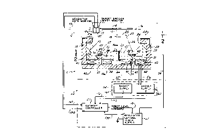
of the power supply 51 may initially switch from a
first level P1 to a second level P2 to maintain the
power levels differently between the inner and outer
regions 94 and 95, respectively. Such levels once
established would be maintained as long as the target
is in its original condition. As the target erodes,
however, these levels may be changed with time as
shown at the right in Fig. 18C. Due to a small amount
of erosion, for example, the inner region 94 is
energized at new level P3, only slightly greater than
level P1 at which it was initially energized. The
outer region 95 is energized at level P4, which may be
substantially greater than its initial level P2 due to
the more serious erosion which may be expected to
occur in the outer region 95.
While the control function is described in
terms of controlling the power from the power supply
51, a measurement of the power parameters of current,
voltage, impedance or a combination of any or all of
these or other related parameters may be used by the
-53-
2~~~~~S
-54-
controller 53 to adjust or modify any of those parame-
ters or other parameters with time. For example, such
measurements may be used to control the intensity or
duration of the current pulses to the magnets shown in
Figs. 18A and 18B and thus the duty cycles of the
respective target regions. In addition, while the
embodiments are described in connection with two
target regions, more than two regions can be con-
trolled in this manner.
10 The waveforms of Fig. 18A-18C illustrate a
controlling of the target emission distribution by
repeatedly alternating the energization of the target
from region to region. It is preferred that the
energizing of the target regions be done repeatedly
15 during the coating of each wafer. The waveforms of
Figs. 18A-18C also illustrate the timing of the
energization of the target regions such that no two
regions are simultaneously energized. In this way,
the sputtering energy expended at each target region
20 can be more readily known; accordingly, such timing is
preferred. Where more than one region is energized
simultaneously, that is, where the waveforms relating
to two regions overlap in time, the power consumed
cannot be related to one region of the target without
25 additional measurement, analysis, or calculation.
Similarly, measurements of electrical operating
parameters are more direct and yield information
-54-
-55-
relating to individual target regions when taken
during times when only one target region is energized.
Accordingly, for appreciation of certain features of
the invention, it is important that each region of the
5 target be energized for some period when no other
region is energized. For the appreciation of many of
the advantages of the present invention it is impor-
taut and preferred that at all times only one region
of the target be energized.
Returning now to Fig. 1, the electrical
control portion of the preferred embodiment of the
present invention can be more fully described. As
Fig. 1 shows, the electrical circuitry 50 includes the
control circuit 53 which contains microprocessor,
15 timers or other appropriate circuitry for performing
the steps described herein. The control circuit or
controller 53 has a pair of analog outputs 172 and 173
which carry signals which determine the timing of
activation and the energization levels far the magnet
20 power supply for alternately onto output lines 55 and
56 which are connected to the magnet windings 41 and
42, respectively.
As illustrated diagrammatically at 176 (Fig.
18), a square wave having a duration T1 in one state
25 and a duration T2 in the other state as controlled by
the circuit 53 applies the waveform 176 to switch the
signals on lines 172 and 173 of the switching circuit
-55-
CA 02001805 1999-OS-19
- 56 -
to alternately switch the magnet power supply output
currents between the lines 55 and 56 in accordance with
that shown in Fig. 18. The waveform 176 is also applied
to the current level outputs 172 and 173 to switch the
current levels between I1 and I2 to deliver the proper
currents I1 and IZ to the respective magnet windings 41
and 42 for respective time periods T1 and T2
The controller 53 includes a microprocessor
171 which has a pair of an output 191 which represents
the desired power levels at which the power supply 51
should energize the target 21 during the respective
portions of the cycle T1 and T2 during which magnets 41
and 42, respectively, are activated. The outputs 55 and
56 of the circuit 52 synchronize the power level setting
at output 191 with the energization of the magnets 411
and 421, respectively, thus regulating the power through
regulation of the voltage of an output amplifier.
CA 02001805 1999-OS-19
- 57 -
The output amplifier, which is contained in
the target power supply 51, switches its output between
the two levels predetermined by the controller 53, in
synchronization with the activation of the magnet 5
windings 41 and 42, respectively. The output amplifier
of the cathode power supply 51 has its output connected
to the output 54 which connects to the target 21. The
cathode power supply 51 also has an output 190 connected
to the controller 53 to communicate such information as
is desired to the controller 53 regarding the actual
power, impedance, current, voltage, or other such
parameter. The controller 53 has control output 191 for
controlling the operation of the power supply 51 will,
in the preferred embodiment be in accordance with the
waveform of Fig. 18C. More particularly, the detected
signal is used to readjust or change the electrical
parameters such as current to the magnet windings 41 and
42 as controlled by outputs 172 and 173, the regulated
levels of operation of the power supply 51, the duty
cycles or duration times TI and T2 or any other
electrically controllable parameters. This control is
done, for example, to fix the uniformity of the
deposition distribution of coating on the substrate 14.
The feedback signal on line 190 may be related
to changes in target geometry due to erosion.
2~~~~~5
-58-
To measure target erosion or sputtering rate, however,
other means are contemplated in accordance with
embodiments of the present invention, such that the
employment of a target deposition rate monitor 194 or
a target erosion depth monitor 195, illustrated in
Fig. 1 having outputs 197 and 198 connected to inputs
of the controller 53. The readjustment of parameters
may be performed by the controller 53 in accordance
with the signals from either lines 190, 197, 198 or
such other signal which is responsive to changes in
parameters, such as a geometric parameter, as for
example, target erosion. In this way, the electrical
parameters, such as I1, I2, T1, T2, or components of
P1 or P2, or other parameters are readjusted.
It should be understood that while the
discussion of this embodiment refers to control of the
power from the power supply 51, other parameters such
as the voltage or the current levels may be controlled
in either similar fashion or may be each otherwise
varied in accordance with the logic of or parameters
predefined within the controller 53.
The erosion depth monitor 195 may be an
adaptation of laser instrumentation technology for
measuring distance, and thus the erosion of, the
. 25 target surface 22 at a region toward which a laser
beam from the monitor 195 is directed. Such a monitor
would be positioned near the substrate.
_58_
CA 02001805 1999-10-14
-59-
The deposition rate monitor 194 may be of a quartz
crystal type known in the sputtering art, or such other type as
may have been or may hereafter be developed. Such a monitor,
positioned near the substrate, measures incident sputtered
material and produces a signal proportional to the sputtering
rate of the target, provided geometric relationships are taken
into account. Such a signal, with the present invention, will
reflect different sputtering rates as different regions of the
target are energized. Thus, the measurement, if synchronized
with the activation of the magnets, will provide information
related to the separate target regions for use in controlling
the operations from the controller 53. Similarly, output
signals on line 190 will be similarly synchronized to target
region activation.
In accordance with the principles of the present
invention, the advantages recited above and others are realized
and improved uniformity in the deposition distribution across
the substrate may be accomplished.
While the ability to isolate and separately measure
various parameters associated with the operation of different
regions of a one piece target has been provided by the present
invention, it is contemplated that other means for monitoring
parameters may be employed or hereafter developed which will
realize
-59-
CA 02001805 1999-OS-19
-60-
the advantages of the present invention. In addition to
or instead of measurement of erosion depth or deposition
rate, cathode current, voltage, impedance and power
measurements, glow discharge spectroscopy, film
reflectivity monitoring, or other such measurements may
be employed. The invention provides particular advantage
for measurements which differ during the respective
energization periods of the target regions to measure
parameters which correspond to the sputtering operation
during such periods.