Note : Les descriptions sont présentées dans la langue officielle dans laquelle elles ont été soumises.
p p ~
2~296~i
Specification
Title of the Invention
Method of Checking Test Program in
Duplex Processing Apparatus
Background of the Invention
The present invention relates to a method of
checking a test program in a duplex processing apparatus
and, more particularly, to a method of checking a test
program executed by a standby system simultaneously with
execution of a program by an active system.
In a conventional duplex processing apparatus, one
of two processors serves as an active processor, and the
remaining processor serves as a standby proces~or. The
active processor reads out instructions and data from its
main memory to perform on-line operations, while the standby
processor executes a test program for checking its
normality.
In a conventional duplex processing apparatus, an
on-line program runs in the memory for the active processor,
and the memories of the active and s~andby systems are
simultaneously updated to duplex the memory contents. A
test program for detecting a failure is executed by the
standby processor simultaneously with execution of the
on-line program by the active processor, thereby preventing
the failure of the standby system.
During checking of the conventional duplex
296~
processing apparatus, when a failure is detected in the
standby system, this is signaled to the active processor.
In this apparatus, no problem is posed when the test program
normally runs. However, for example, wh~n the standby test
program has a failure or overruns due to hardware fault or a
software bug, a on-line memory area of the standby processor
may be broken. Under this circumstance, since the tes-t
pro~ram itself overruns, and the standby processor cannot
acknowledge the failure to the active processor. As a
result, system reliability is adversely degraded.
Summary of the Invention
It is, therefore, a principal object of the
present invention to provide a method of checking a test
program in a duplex processing apparatus which can improve
system reliability.
In order to achieve the above object of the
present invention, there is provided a method of checking a
test program in a duplex processing apparatus comprising two
processors connected to each other through a failure
acknowledge line and an interprocessor communication line
and constituting an active system and a standby system, main
memories connected to the two processors through buses,
respectively, a queue connected to the buses which connect
the processors to the main memories, and bus arbitors for
controlling contention of a bus occupy right on the buses,
comprising checking normality of the test program from an
execution address of the test program executed by the
-- 2
2~Z96~
standby processor under the control of the active processor.
Brief Description of the Drawings
Fig. 1 is a block diagram of a duplex processing
apparatus according to an embodiment of the present
invention;
Figs. 2A and 2B are data formats of active and
standby memories shown in Fig. 1, respectively;
Fig. 3 is a detailed block diagram of the duplex
processing apparatus shown in Fig. l; and
Fig. 4 is a flow chart for explaining a program
for causing an active processor to monitor a running state
of a standby failure detection program.
DESCRIPTION OF THE PREFERRED EMBODIMENT
A preferred embodiment of the present invention
will be described in detail with reference to the
accompanying drawings.
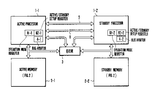
Fig. 1 shows an arrangement of a duplex processing
apparatus according to an embodiment of the present
invention.
Referring to Fig. 1, reference numerals 1-1 and
1-2 denote active and standby processors or 0- and l-systems
each incorporating a CPU; 2-1 and 2-2, active and standby
memories, respectively. Reference numeral 3 denotes a queue
for updating the memories. Reference numerals 4-1 and 4-2
denote active and standby bus arbitors contained in the
active and standby processors 1-1 and 1-2, respectively.
Reference numeral 5 denotes a failure acknowledge
- 3 -
., .
.:
- : ,.
929~6
line; 6, an interprocessor communication line for causing
the processors 1-1 and 1-2 to directly exchange data
therebetween.
The contents of the active and standby memories
2-1 and 2-2 shown in Fig. 1 are shown in Figs. 2A and 2B,
respectively. Each memory has a diagnostic program area A
and an on-line area B. In this embodlment, an area from
address 0 to address 1000 serves as the diagnostic program
area A, and a diagnostic program is stored therein. An area
from address 1001 to address 100000 serves as the on-line
area B, and an on-line program is stored therein. During
synchronous operation, the memory 2-1 is updated by a memory
write request generated upon execution of the active on-line
program. For this reason, the data at the addresses
identical with those of the memory 2-1 are also updated in
the standby memory 2-2. However, the program is created not
to update the data in the diagnostic program area A at
addresses 0 to 1000 of the memory 2-2. That is, the on-line
program should not access the diagnostic program area of the
memory 2-2. The standby diagnostic program stored in the
area B of the standby memory 2-2 at addresses 0 to 1000 is
executed to check normality of standby hardware. When a
failure is detected, a standby failure is acknowledged as an
interrupt to the active processor 1-1 through the failure
acknowledge line 5. Upon reception of the interrupt, the
active system detects the failure of the standby system and
disconnects the standby system by changing the operation
-- 4
~., : . .
,
Z~29~
mode from the synchroniæation mode to an asynchronization
mode.
In the synchronization mode, when a memory write
request is generated by the active system, a write address
signal and a data signal are written in the queue 3 arranged
between the mating processors 1-1 and 1-2. The standby
memory 2-2 is updated by the standby bus arbitor 4-2 using
an empty area of a standby memory bus in accordance wi-th the
content of the queue 3.
In the asynchronization mode, a memory write
operation from the active system to the standby memory 2-2
is not performed. The synchronization/asynchronization mode
is set by an operation mode register Rl-l (one bit) in the
active processor 1-1. The active/standby mode is set by an
active/standby setup register R2-1 in the active system.
When logic "0" is set in the register R2-1, a 0-system
processor is active, and a l-system processor is standby.
When the active/standby setup register R2-1 of the active
system is set at logic "1", the 0-system processor is
standby, and the l-system processor is active. In this
case, a register R2-2 stores an inverted content of the
register R2-1.
Operation mode registers Rl-l and Rl-2 and the
active/standby setup registers R2-1 and R2-2 can be set in
accordance with a program.
Fig. 3 shows a detailed arrangement of the duplex
processing apparatus shown in Fig. 1 and, particularly, a
-- 5
' ' ' ~ , ' ,'" ,
2~
detailed arrangement of the queue 3. Referring to Fig. 3,
reference numerals 31-1 and 31-2 denote input selectors;
32-1 and 32-2, output selectors; 33, an address queue; 3~, a
data queue; and 35, a queue controller.
Reference symbol Sl denotes a stop request line
for sending a request for stopping -the opposite processor
between the active and standby processors 1-1 and 1-2.
Reference symbol S2 denotes a signal line for reading a stop
address signal of the opposite processor between the active
and standby processors 1-1 and 1-2. These signal lines Sl
and S2 are represented as the interprocessor communication
line in Fig. 1.
Reference symbols Bl-l and Bl-2 denote control
buses for connecting the active and standby processors 1-1
and 1~2 to the queue 3 and transmitting control data
therebetween. Reference symbols Dl-l and D1-2 denote data
buses for connecting the active and standby processors 1-1
and 1-2 to the queue 3 and transmi-tting data signals
therebetween. Reference symbols Al-l and Al-2 denote
address buses for connecting the active and standby
processors 1-1 and 1-2 to the queue 3 and transmitting
address signals therebetween.
Reference symbols S5-1 and S5-2 denote bus enable
signal lines for connecting the queue controller 35 in the
queue 3 to the active and standby processors 1-1 and 1-2 and
sending a bus enable signal for assigning a bus occupy right
from the active or standby processor 1-1 or 1~2. Reference
,~
~2002~96~D
symbols S6-1 and S6-2 denote bus occupy signal lines for
connecting the queue controller 35 to the active and standby
processors 1-1 and 1-2 and sending a bus occupy signal to
the active or standby processor 1-1 or 1-2.
The input selectors 31-1 and 31-2 of the queue 3
write address and data signals required for write access in
the address queue 33 and the data queue 34 through the
address bus Al-l and the data bus Dl-l under the control of
the queue controller 35 when, e.g., the 0-system is active.
The address and data signals written in the address queue 33
and the data queue 34 are sent onto the standby address bus
Al-2 and the standby data bus Dl-2 through the output
selector 32-1 under the control of the queue controller 35
and are written in the standby memory 2-2. In this case,
the bus occupy signal is sent from the queue controller 35
to the CPU of the standby processor 1-2 so as to prevent a
conflict with memory access of the diagnostic program
executed by the standby system. A bus enable signal is sent
from the CPU of the processor 1-2 onto the bus enable line
S5-2. Upon reception of this bus enable signal, the address
and data signals written in the address queue 33 and the
data queue 34 are written in the standby memory 2-2. Note
that the operation mode registers Rl-l and Rl-2 and the
active/standby setup registers R2-1 and R2-2 control the
25 input selectors 31-1 and 31-2 and the output selectors 32-1
and 32-2 of the queue 3 through the queue controller 35.
- . ............... . : . :
..
In the above arrangement, the processor 1-1 is
active, and the processor 1-2 is standby.
The active processor 1-1 reads out an instruction
and data from the memory 2-1 and executes the on-line
program. In the write mode, both the memories 2-1 and 2-2
are updated. In this case, the write address and data
signals are simultaneously stored in the queue 3.
The queue 3 autonomously outputs the address and
data signals. After the queue 3 obtains a communication
right with the standby memory 2-2 by means of the bus
arbitor 4-2, write access of the memory 2-2 is performed.
The standby processor 1-2 stores the failure
detection program in an area which does not overlap the
on-line area in the memory 2-2. The standby processor 1-2
performs the failure detection program simultaneously with
and independently of the operation of the active processor
1 1. When a failure of the standby system is detected, the
failure detection program sends an interrup-t to the active
processor 1-1 through the failure acknowledge line 5.
The following program sequence is performed to
cause the active system to monitor a running state of the
standby failure detection program. The flow chart of this
,,1 program se~uence is shown in Fig. 4.
'~ The active processor 1-1 checks in step 100
whether the standby failure detection program is running.
This check operation is initiated once every minute. If
this check operation is successful, the flow advances to
-- 8
.
.,- , - . . , :
. . ~ - , ,
21[)C~29~6
step 101 to stop the standby system. The active processor
1-1 sends a command to the standby processor 102 through the
line 6. If the program stops in step 100, the flow advances
to step 107 (to be described later~ to set the
asynchronization mode.
The active processor 1-1 checks in step 102
whether the standby system is successfully stopped. If the
standby system is successfully stopped, the flow advances to
step 103. A standby stop address X is sent to the active
system. The active processor 1-1 checks in step 104 whether
the stop address X falls within a predetermined range (e.g.,
0 to 1000 in this embodiment) in accordance with memory
assignment information of the failure detection program. If
YES in step 104, the active processor 101 executes the
on-line program, and the flow advances to step 105 to
continue the failure detection program.
However, if the stop of the standby system fails
in steps 100, 102, and 104, the flow advances to step 107 to
set the operation mode register R1-1 in the asynchronization
mode. The flow then advances to step 108 to start the
program for diagnosing the standby system. Note that
processing from connector ~ is started if a failure other
than the above failure is acknowledged from the standby
system in Fig. 4.
According to the present invention, as has been
described above, the standby failure detection function can
... . . .
32~
be guaranteed, thereby providing a duplex processing
apparatus having improved system reliability.
.
- 10 -