Note : Les descriptions sont présentées dans la langue officielle dans laquelle elles ont été soumises.
2003471
IMPROVED FEED WAVEGUIDE FOR AN ARRAY ANTENNA
BACKGROUND OF THE INVENTION
Field of the Invention:
The present invention relates to slot array
antennas. More specifically, the present invention
relates to an improved feed for a slot array antenna.
While the present invention is described herein with
reference to an illustrative embodiment for a particular
application, it is understood that the invention is not
limited thereto. Those of ordinary s~ill in the art and
access to the teachings provided herein will recognize
additional modifications, applications and embodiments
within the scope thereof.
~escription of the Related Art:
Planar array ant~nn~ are used for a wide variety of
radar applications. One such planar array antenna is a
flat plate antenna. A flat plate antenna is typically a
family of coplanar linear arrays each containing a series
of resonant slot radiating apertures. Microwave energy is
provided to the radiating waveguides by a feed waveguide
which is in turn fed by an input waveguide.
Slot coupling is a desirable technique for coupling
energy from the feed waveguide to the radiating
waveguides for most applications. Slot coupling, for a
single feed, involves communication of energy through a
slot in a broadwall of a rectangular feed waveguide and
,~
2003A7~
_ 2
slots in a broadwall of a rectangular radiating
waveguide. Energy is typically provided to the feed
waveguide by an input waveguide located at either end of
the feed waveguide or somewhere along the length thereof.
The location of the input waveguide at the ends of
the feed waveguide may limit the bandwidth of the system
or be otherwise problematic because of the relative
inaccessibility of the ends of the feed waveguides.
The center feeding of the feed waveguide is
problematic with respect to the location of the input
slot of the input waveguide relative to the feed slot of
the feed waveguide. That is, if, as is common, the input
slot and the feed slots are placed on opposite broad
walls of the feed waveguide and at one-quarter wavelength
spacing down the waveguide, an impedance inversion
results on each half of the feed waveguide which must be
corrected in the design. A common technique for
- correcting the impedance inversion involves a design in
which coupling slots are at greater angles.
Unfortunately, this approach typically results in larger
coupling junction phase errors.
Location of the input slots on the opposite
broadwall at the same position along the length of the
feed waveguide as the feed slots has heretofore been
avoided because of difficulty in achieving independent
coupling of the input slot and the opposite feed slot.
There is therefore a need in the art for a planar
array antenna feed waveguide which has an input slot
located between the ends of the waveguide but does not
have any associated impedance inversion.
20034~1.
SUMMARY OF THE Ihv~NllON
The need in the art for a feed waveguide design that
reduces coupling junction phase errors is addressed by
the improved feed waveguide of the present invention. The
improved feed waveguide of the present invention includes
first and second slotted parallel walls. The first wall
includes a first elongate slot along a first longitll~i n~ 1
axis. The second wall includes a second elongate slot
located on the second wall opposite the first slot on the
first wall. The second slot has a second longitudinal
axis .
In a particular embodiment, the invention is adapted
to provide a planar array antenna including at least one
radiating waveguide having a first broadwall with a first
elongate slot therethrough and a first longitudinal axis.
A feed waveguide is coupled to the radiating waveguide
and has first and second parallel walls along the length
thereof. The first wall has a second elongate slot
therethrough which is in communication with the first
slot in the radiating waveguide. The second slot has a
longitudinal axis and is aligned with the slot in the
radiating waveguide. A third slot is located in the
second wall opposite the second slot in the first wall
and has a second longitudinal axis. An input waveguide
is coupled to the feed waveguide and includes a broadwall
with an elongate slot therethrough. The slot in the
input waveguide is in communication with the third slot
in the feed waveguide. The slot in the input waveguide
has a longitudinal axis aligned with the longitudinal
axis of the third slot. Thus, in accordance with the
present teachings, the slot in the input waveguide is
colocated with the slot in the radiating waveguide and
orthogonal thereto. This arrangement mitigates impedance
~ 4
200347 1
inversion and allows for optimum performance of an array
antenna.
Another aspect of this invention is as follows:
A planar array antenna comprising:
at least one radiating waveguide having a first
broadwall with a first elongate slot therethrough having
a first longitudinal axis passing through a center of
said first elongate slot;
a feed waveguide having first and second parallel
walls along the length thereof, said first parallel wall
having second elongate slot therethrough positioned
adjacent to said first elongate slot and having a second
longitudinal axis passing through a center of said
second elongate slot and parallel with said first
longitudinal axis and said second parallel wall having a
third elongate slot therethrough located opposite said
second elongate slot and having a third longitudinal
axis passing through a center of said third elongate
slot;
an input waveguide having a broadwall with a fourth
elongate slot therethrough positioned adjacent to said
third elongate slot and having a fourth longitudinal
axis passing through a center of said fourth elongate
slot, wherein the centers of said first, second, third
and fourth elongate slots are aligned along a vertical
z-axis such that the first, second, third and fourth
slots are in alignment permitting the coupling of energy
from said input waveguide to said feed waveguide without
impedance; and
said fourth longitudinal axis of said fourth
elongate slot in said input waveguide is orthogonal to
said second longitudinal axis of said second elongate
slot in said feed waveguide.
'C
~ 4a 200347 t
BRIEF DESCRIPTION OF THE DRAWINGS
Fig. l(a) is an illustrative representation of a
top view of a section of a flat plate slot array antenna
incorporating the principles of the present invention.
Fig. l(b) is an illustrative representation of a
- sectional side view of a section of a flat plate slot
array antenna incorporating the principles of the
present invention.
Fig. l(c) shows a side view of a feed waveguide in
a section of a flat plate slot array antenna
incorporating the principles of the present invention.
Fig. 2(a) shows a prior art feed waveguide wherein
the feed waveguide is fed via an input slot on one wall
of the waveguide which is located between a series of
feed slots which lie on the opposite wall of the feed
waveguide.
Fig. 2(b) shows a end view of the feed waveguide of
Fig. 2(a).
Fig. 3 shows the present invention feed waveguide
wherein the feed waveguide is fed via an input slot on
one wall of the feed waveguide and colocated with one of
a series of feed slots on the opposite wall of the feed
waveguide.
Fig. 4 is an expanded view showing the location of
an input slot and a colocated feed slot in the feed
waveguide of the present invention.
` . 2003471.
DESCRIPTION OF THE INVENTION
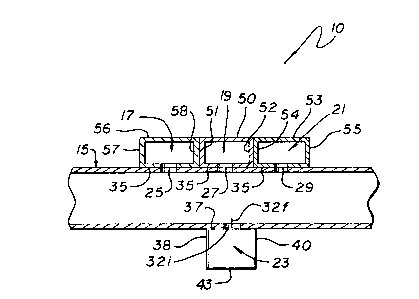
Fig. l(a) is a top view of a section of the flat
5 plate slot array antenna 10, incorporating the principles
of the present invention. The section of the antenna 10
includes first, second and third radiating waveguides 17,
19 and 21, respectively, mounted orthogonal to a feed
waveguide 15 in broadwall-to-broadwall relation. Each
10 waveguide may be of conventional fabrication, e.g., metal
or other suitably conductive material. The radiating
waveguides 17, 19 and 21 are spaced along the
longitudinal axis of the feed waveguide 15 and coupled
thereto by a plurality of inclined slots (shown in
phantom) 25, 27 and 29 respectively. The radiating
waveguides 17, 19 and 21 are spaced so that they lie
directly next to one another.
As shown in the sectional side view of Fig. l(b),
each radiating waveguide is rectangular having first and
second broadwalls and first and second sidewalls. For
example, the second radiating waveguide 19 has first and
second broadwalls 35 and 50 and first and second
sidewalls 51 and 52. Similarly, the feed waveguide 15
includes a front broadwall 35, a back broadwall 37 and
side walls 46 and 48. (See the end view of Fig. l(c).)
A rectangular input waveguide 23 is mounted on the back
broadwall 37 of the feed waveguide 15 and includes a
front broadwall 43, a back broadwall 32 and sidewalls 38
and 40.
The radiating waveguides 17, 19, and 21 are mounted
on the front broadwall 35 of the feed waveguide 15. The
feed waveguide 15 is coupled to the radiating waveguides
by a plurality of elongate inclined feed slots 25, 27,
and 30, in the front broadwall 35 of the feed waveguide
15. Each of the radiating waveguides 17, 19 and 21
- Z003471.
_ 6
contains a plurality of radiating slots which receive the
energy from the feed slots 25, 27 and 29, respectively.
Each of the radiating slots are spaced one-half
wavelength from each neighboring radiating slot. The
radiating waveguide 17 contains the radiating slots 71,
72, 73, 74, 75 and 76. The radiating waveguide 19
contains the radiating slots 77, 78, 79, 80, 81 and 82.
The radiating waveguide 21 contains the radiating slots
83, 84, 85, 86, 87 and 88. Each of the feed slots 25, 27
and 29 lie equidistant between two radiating slots. Thus,
there is a one-quarter wavelength spacing from each feed
slot and the closest radiating slot. Each feed slot 25,
27, and 30 is inclined with respect to a longitudinal
axis 39 of the feed waveguide 15 and has a longitudinal
axis 41, 44, and 45 respectively. The feed slots 25, 27
and 29 are shown in phantom in Fig. l(a).
The feed waveguide 15 also includes an input slot 32
on the back wall 37 thereof. The input slot 32 is
provided by a slot 32f in the feed waveguide 15 and a
slot 32i in an input waveguide 23. The input slot 32 is
also inclined with respect to the longitu~;nAl axis 39
of the feed waveguide 15 and has a longitll~;n~l axis 42.
As discussed below, a particularly novel feature of the
present invention is the colocation of the input slot 32
with the feed slot 27 along the longitudinal axis 39 of
the feed waveguide 15. The colocation of the input slot
32 relative to a feed slot 27 allows for the coupling of
energy from the input waveguide 23 to the feed waveguide
15 without an impedance inversion. The colocation of the
input slot 32 with a feed slot 27 is permitted by the
orthogonal arrangement of the input slot 32 relativé to
the feed slot 27. That is, the longitudinal axis 42 of
the input slot 32 is orthogonal to the longitudinal axis
44 of the feed slot 27. (This is illustrated more
clearly in phantom in Fig. l(a).) Thus, energy is
2003471.
provided to the feed waveguide 15 by the input waveguide
23 via the slot 32. The feed waveguide 15 then couples
the energy to the radiating waveguides 17, 19 and 21 via
slots 25, 27 and 29 on the broadwall 35. The energy is
then radiated to the atmosphere by the radiating
waveguides 17, 19 and 21 in a conventional manner.
The advantageous design of the improved feed
technique of the present invention is appreciated with
reference to the conventional feed arrangement of Fig.
2(a). Fig. 2(a) is an illustrative representation of a
conventional feed waveguide 15' which is fed via an input
slot 32' located between the ends of the feed waveguide
15'. Fig. 2(b) is a side view of the conventional feed
waveguide 15' showing the front and back broadwalls 35'
and 37', respectively. The conventional feed waveguide
15' includes a plurality of feed slots 25', 27', 2g', on
the front broadwall 35' of the feed waveguide 15'
inclined with respect to the longitudinal axis 39'
thereof and the input slot 32' (shown in phantom) on the
back broadwall 37' of the feed waveguide 15'. The input
slot 32' has a longitudinal axis 70 which is generally
normal to the longitudinal axis 39' of the feed waveguide
15'. The two feed slots 25' and 27' are generally
separated by a distance of one half of the wavelength of
the operating frequency. The input slot 32' is located
on the back broadwall 37' of the feed waveguide 15'
between two feed slots 25' and 27' on the front
broadwall 35' thereof. The input slot 32' is located
equidistant between the two feed slots 25' and 27'.
There is therefore a one-quarter wavelength spacing
between the input slot 32' and each of the two feed
slots 25' and 27'. The one-quarter wavelength spacing
between the feed slots 25' and 27' and input slot 32'
causes a one-quarter wave inversion in the characteristic
3S impedance of the waveguide each half of the feed
2003a~71.
waveguide 15'. This has previously precluded the
centerfeeding of feed waveguides for many conventional
planar array ant~nn~c.
As mentioned in the Background of the Invention, an
alternate conventional method of feeding the waveguide
15' is via either end of the feed waveguide 15'. The
advantage of the design is that impedance inversion is
avoided. However, as previously discussed, the location
of the input waveguide at the ends of the feed waveguide
15' may limit the bandwidth of the system or be otherwise
problematic because of the relative inaccessibility of
the ends of the feed waveguide 15'.
Fig. 3 is top view of the feed waveguide 15
constructed in accordance with the principles of the
present invention. As mentioned above, the input slot 32
is colocated with a feed slot 27 and orthogonal thereto.
The is effective to mitigate the impedance inversion. A
direct consequence of which is that smaller values of
coupling slot angles can be used which, in turn, reduces
coupling junction phase errors.
The expanded view of Fig. 4 better illustrates the
advantageous location of an input slot 32 and a colocated
feed slot 27 of a section of a feed waveguide 15 of the
present invention. The input slot 32 is shown in phantom
to indicate that it is located on the bottom broadwall 37
of the feed waveguide 15. The feed slot 27 is located on
the top broadwall 35 of the feed waveguide 15. Both the
input slot 32 and the feed slot 27 are inclined with
respect to the longitudinal axis 39 of the feed waveguide
15. The input slot 32 has a longitudinal axis 42 which is
orthogonal to the longitudinal axis 44 of the feed slot
27. The input slot 32 couples energy from an input
waveguide to the feed waveguide 15. The feed slot 27
couples energy from the feed waveguide 15 to a radiating
waveguide.
200~47~.
g
Those skilled in the art will appreciate that
an improved feed waveguide design has been disclosed
which provides a reduction of coupling junction phase
er~ors. Although the present invention has been described
S with reference to a particular illustrative embodiments
for particular illustrative applications, those of
ordinary skill in the art, having access to the present
teachings, will recognize additional modifications,
applications, and embodiments within the scope thereof.
For example, the number and orientations of the inclined
slots is not critical to the invention. And while the
invention is described with reference to a planar array
antenna, the present invention is not limited thereto.
The feed arrangement of the present invention is also
advantageous in a linear array antenna such as a small
Ka-band flat plate antenna. In addition, common forms of
input slot excitation may be utilized in connection with
present teachings.
It is intended by the appended Claims to cover any
and all such modifications, applications, and embodiments
within the scope of the invention.