Sélection de la langue

Search

Sommaire du brevet 2003831 

Énoncé de désistement de responsabilité concernant l'information provenant de tiers

Une partie des informations de ce site Web a été fournie par des sources externes. Le gouvernement du Canada n'assume aucune responsabilité concernant la précision, l'actualité ou la fiabilité des informations fournies par les sources externes. Les utilisateurs qui désirent employer cette information devraient consulter directement la source des informations. Le contenu fourni par les sources externes n'est pas assujetti aux exigences sur les langues officielles, la protection des renseignements personnels et l'accessibilité.

Disponibilité de l'Abrégé et des Revendications

L'apparition de différences dans le texte et l'image des Revendications et de l'Abrégé dépend du moment auquel le document est publié. Les textes des Revendications et de l'Abrégé sont affichés :

  • lorsque la demande peut être examinée par le public;
  • lorsque le brevet est émis (délivrance).
(12) Demande de brevet: (11) CA 2003831
(54) Titre français: APPAREIL DE COMMUNICATION RADIO
(54) Titre anglais: RADIO COMMUNICATION APPARATUS
Statut: Réputée abandonnée et au-delà du délai pour le rétablissement - en attente de la réponse à l’avis de communication rejetée
Données bibliographiques
(51) Classification internationale des brevets (CIB):
  • H04B 01/04 (2006.01)
(72) Inventeurs :
  • YONEI, YOSHIYUKI (Japon)
  • YONEI, YOSHIYUKI (Japon)
(73) Titulaires :
  • YOSHIYUKI YONEI
  • YOSHIYUKI YONEI
(71) Demandeurs :
(74) Agent: BORDEN LADNER GERVAIS LLP
(74) Co-agent:
(45) Délivré:
(22) Date de dépôt: 1989-11-24
(41) Mise à la disponibilité du public: 1990-05-28
Licence disponible: S.O.
Cédé au domaine public: S.O.
(25) Langue des documents déposés: Anglais

Traité de coopération en matière de brevets (PCT): Non

(30) Données de priorité de la demande:
Numéro de la demande Pays / territoire Date
63-301735 (Japon) 1988-11-28

Abrégés

Abrégé anglais


ABSTRACT
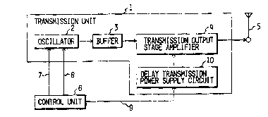
The invention provides a radio communication apparatus, which includes
means for preventing unwanted and unnecessary radiation at the start of a
radio transmission. The apparatus of the present invention has a simple delay
circuit for slowly increasing the voltage applied to an amplifier in a
transmission unit including an oscillator, which generates a high-frequency
signal of a desired carrier, a buffer, and the amplifier to which is input the
high-frequency signal from the oscillator via the buffer and which amplifies
the signal and transmits data via an antenna. The delay circuit is connected
to a voltage line applied to the amplifier and slowly increases the voltage at
the start of the radio wave transmission. The input impedance of the
amplifier is prevented from sharply changing and is only allowed to change
slowly. The change of the input impedance of the amplifier is translated into
a change of load impedance of the oscillator, the amount of such impedance
change being decreased by the operation of the buffer. Thus, it is possible
to prevent the generation of unnecessary radiation at the start of the radio
wave transmission.

Revendications

Note : Les revendications sont présentées dans la langue officielle dans laquelle elles ont été soumises.


THE EMBODIMENTS OF THE INVENTION IN WHICH AN EXCLUSIVE PROPERTY OR PRIVILEGE
IS CLAIMED ARE DEFINED AS FOLLOWS:
1. A radio communication apparatus comprising:
a transmission unit having
oscillation means for generating a high-frequency signal of a desired
carrier wave,
amplifier means for amplifying said high-frequency signal,
buffer means for preventing said high-frequency signal from
fluctuating due to changes of load of said amplifier means, and
delay means for constraining a voltage applied to said amplifier
means at the start of radio transmission to a rate of rise in which such
voltage change does not cause said high-frequency signal of said
oscillation means to fluctuate; and
control means for commanding said oscillation means so as to generate said
high-frequency signal of said desired carrier wave and for commanding said
delay means to operate after stabilization of said high-frequency signal.

Description

Note : Les descriptions sont présentées dans la langue officielle dans laquelle elles ont été soumises.


. ~003831.
Rl~DIO COMHUNICATION APPARAllJS
The present invention relates to a radio communication apparatus
capable of keeping one radio transmitter from interfering with another when
a plurality of adjoining radio transmitters are simultaneously transmitting
radio waves.
In a radio communication system having a plurality of radio
communication apparatuses capable of simultaneous communication, the
unwanted xadiation generated by one radio communication apparatus at the
start of radio transmission interferes with data transmission of other
apparatuses while the plurality of adjoining radio communication apparatuses
are carrying on communication simultaneously.
A radio communication apparatus generally comprises an oscillator for
generating a high-frequency signal of a carr~er wfive and an amplifier to --~
lS amplify the high-frequency signal. Conventionally, a buffer is placed
between the oscillator and the amplifier to reduce imped~nce changes seen
from the oscillator in order that changes in the input impedance of the
amplifier may not be translated directly into changes of load on the
oscillator when the power ~upply of the amplifier is switched from OFF to ON
or from ON to OFF.
The buffer i8 generally composed of an isolator, an attenuator, a
buffer amplifier or a combination of these.
However, the prior art has various disadvan~ages, including the fact
that ~he buffer circuit itself is bulky because the buffering capability
required for the buffer i8 high and this detracts from any attempts to make
the radio~transmitter compact and to reduce manufacturing cost.
If an isolator having high buffering capability i8 used, for instance,
the buffer i~ not suitable for general purpose use because its usable
frequency band is extremely narrow and is a relatively eYpensive product
30 because it isldifficultl,to luse it lin common with other models as a means of -
reducing co~t. As for an attenuator, on the other hand, its buffering ~ -
capability~improves~as the amount of attenuation is increased. However,
increased amplification is required to make up ~or the attenuation of the
attenuator, in order to obtain the same transmission power, which mitigates .
against reduction in power consumption.
PAT 15176~

Z003831
An object of the present invention i9 to provide a radio communication
apparatus, which includes means for preventing unwanted snd unneceissary
radiation at the start of a radio transmission.
Another object of the present invention is to provide a relatively
small and low-priced radio communication apparatus by utilizing a simple
circuit to prevent such spurious radiation.
To realize the above objects, the radio communication apparatus of the
present invention has a simple delay circuit for slowly increasing the
voltage applied to an ampllfisr in a transmission unit including an
oscillator, which generates a high-frequency signal of a desired carrier, a
buffer, and the amplifier to which is input the high-frequency signal from
the oscillator via the buffer and which amplifies the signal and transmits
data via an antenna.
The delay circuit is connected to a voltage line applied to the
amplifier and slowly increases the voltage at the start of the radio wave
transmission. The input impedance of the amplifier is prevented from
sharply changing but is only allowed to change slowly. The change of the
input impedance of the amplifier is translated into a change of load
impedance of the oscillator, the amount of such impedance change being
20 decreased by the operation of the buffer. Thus, it is possible to prevent ~-
~; ~the generation of unnecessary radiation at the start of the radio wave
transmission.
It may be noted that the delay time ~T should be 1 .TN (TN - 2-
~or more, when the oscillator consists of a frequency synthesizer using ~ L
circuits and has a natural frequency of WN.
The invention vill now be described further by way of eYample only and ~;
with reference to the accompanying drawings, wherein:
Fig. 1 is a block diagram illustrating transmission and control units
of a radio communication apparatus embodying the present invention;
30 ~ i Fig. 2 is~a circuit diagram illustrating a first example of a
transmission power supply circuit with delay, embodying the present
invention; and
Fig. 3 i8 a circuit diagram illustrating a second eYample of a
transmission power supply circuit with delay, embodying the present
- 35 invention.
PAT 15175-1
~:- : ,

20038~1
Referring to the accompanying drawings, and particularly to Fig. 1, a
transmission unit 1 has an oscillator 2, a buffer 3, a transmission output
stags amplifier 4, and a transmission power supply circuit 10 having
built-in delay. An output of the oscillator 2 is inputted to the
transmission output stage amplifier 4 via the buffer 3. The output of the
transmission output stage amplifier 4 i9 connected to an antenna S.
A control unit 6 sends out a frequency specifying signal 7 and a data
signal 8 to the osclllator 2, and a transmission power supply control signal
9 to the transmission power supply circuit 10.
In operation, the control un~t 6 sends out the frequency specif~ing
signal 7 to determine the oscillation frequency of the oscillator 2 when the
radio communication apparatus starts transmission. The oscillator 2 thereby
oscillates to provide a high frequency signal of a desired carrier frequency
at a predetermined time later. The control unit 6 subsequently sends out
the transmission power supply control signal 9 to the transmission power
supply circuit 10 with the predetermined passage of time needed to stabilize
the oscillation frequency of the oscillator 2 and applies the power supply
voltage to the transmission output stage amplifier 4. At this time, the
power supply voltage applied to the transmission output stage amplifier 4 is
prevented from sharply rising but allowed to rise slowly because of the
delaying operation of the transmission power supply circuit 10. In this
way, as the power supply voltage applied to the transmission output stage
`~ ampllfier 4 ~lowly changes from OFF to ON, the input impedance of the
transmission output stage amplifier 4 is also prevented from sharply ;~
changing but is allowed to change slowly. The change of the input impedance
of~the transmission output stage amplifier 4 is translated into a change of
load impedance of the oscillator 2 while the amount of the impedance change
is reduced by the operation of the buffer 3. With this arrangement, the
buffer 3 makes it possible to prevent the generation of unnecessary
~ 30 radiation at the start!,of radio waye transmission without using
- sophisticated devices or circuits.
Referring still to the drawings, the transmission power supply circuit
- embodying the present invention will now be described.
,rF,~
~ PAT 151~6~

~-` 2003831
In Fig. 2, an IC 21 is a stabilized power supply IC having a voltage
comparison input terminal. Input voltage 24 i8 applied to IC 21 when a
switch 22 is in it6 stationary closed state and the output of the IC 21 is
divided by voltage dividing resistors R2, R3 and received by a voltage
comparison input terminal of the IC 21 for comparison with a reference
voltage, so that a stabilized output voltage 25 is obtained.
Assume a transmission power supply control signal 23 i9 suddenly
applied, which closes the switch 22. Voltage appears at the output terminal
of the IC 21 because input voltage 24 is now applied to the IC 21. However,
the instantaneous operation of series-connected resistor Rl and capacitor C
(see Fig. 2) causes the voltage dividing resistor R2 to be bypassed and the
voltage divided by the resistor Rl and the voltage dividing resistors R2, R3
is applied to the voltage comparison input terminal of the IC 21.
Consequently, the IC 21 is controlled so that the rate of increase in output
voltage is reduced. As a result, the net effect upon the output voltage 25
is that it rises slowly instead of sharply.
Fig. 3 shows an IC 31 which is a 3-terminal regulator and is used as a
constant-voltage power supply. ~hen a transmission power supply control
signal 33 i8 applied to close switch 32, input voltage 34 is applied to the
20 IC 31 and output voltage 35 is integratet by the output impedance of the IC ~ -
31 and the capacitance of a capacitor Cl, to provide slow rising
characteristics.
As set forth above, the radio communication apparatus according to the
present invéntion has the transmission power supply circuit designed with a
25~ built-in delay to make the pover supplied to the transmission output stage ~ -
amplifier have slow rising characteristics, whereby it is possible to
prevent~the generation of the unwanted radiation at the start of radio wave
transmission~and to free other transmitte~s from interference.
AI 15176~

Dessin représentatif
Une figure unique qui représente un dessin illustrant l'invention.
États administratifs

2024-08-01 : Dans le cadre de la transition vers les Brevets de nouvelle génération (BNG), la base de données sur les brevets canadiens (BDBC) contient désormais un Historique d'événement plus détaillé, qui reproduit le Journal des événements de notre nouvelle solution interne.

Veuillez noter que les événements débutant par « Inactive : » se réfèrent à des événements qui ne sont plus utilisés dans notre nouvelle solution interne.

Pour une meilleure compréhension de l'état de la demande ou brevet qui figure sur cette page, la rubrique Mise en garde , et les descriptions de Brevet , Historique d'événement , Taxes périodiques et Historique des paiements devraient être consultées.

Historique d'événement

Description Date
Inactive : CIB expirée 2015-01-01
Inactive : CIB de MCD 2006-03-11
Inactive : Demande ad hoc documentée 1996-11-25
Inactive : Abandon.-RE+surtaxe impayées-Corr envoyée 1996-11-25
Demande non rétablie avant l'échéance 1992-05-24
Le délai pour l'annulation est expiré 1992-05-24
Inactive : Demande ad hoc documentée 1991-11-25
Réputée abandonnée - omission de répondre à un avis sur les taxes pour le maintien en état 1991-11-25
Demande publiée (accessible au public) 1990-05-28

Historique d'abandonnement

Date d'abandonnement Raison Date de rétablissement
1991-11-25
Titulaires au dossier

Les titulaires actuels et antérieures au dossier sont affichés en ordre alphabétique.

Titulaires actuels au dossier
YOSHIYUKI YONEI
YOSHIYUKI YONEI
Titulaires antérieures au dossier
S.O.
Les propriétaires antérieurs qui ne figurent pas dans la liste des « Propriétaires au dossier » apparaîtront dans d'autres documents au dossier.
Documents

Pour visionner les fichiers sélectionnés, entrer le code reCAPTCHA :


Pour visualiser une image, cliquer sur un lien dans la colonne description du document. Pour télécharger l'image (les images), cliquer l'une ou plusieurs cases à cocher dans la première colonne et ensuite cliquer sur le bouton "Télécharger sélection en format PDF (archive Zip)" ou le bouton "Télécharger sélection (en un fichier PDF fusionné)".

Liste des documents de brevet publiés et non publiés sur la BDBC .

Si vous avez des difficultés à accéder au contenu, veuillez communiquer avec le Centre de services à la clientèle au 1-866-997-1936, ou envoyer un courriel au Centre de service à la clientèle de l'OPIC.


Description du
Document 
Date
(aaaa-mm-jj) 
Nombre de pages   Taille de l'image (Ko) 
Revendications 1990-05-27 1 71
Abrégé 1990-05-27 1 107
Dessins 1990-05-27 1 37
Description 1990-05-27 4 427
Dessin représentatif 1999-07-25 1 8