Note : Les descriptions sont présentées dans la langue officielle dans laquelle elles ont été soumises.
- X004~65
.
CM00703J
.- REAC~!ANCE BUFli'lZRED LOOP ANT~NNA
AND ~ICTYOD FO~ ~ RING T~lC 8A~IC
FI~ OF 'rHE; TNVEN~
This invention relates generally to the field of loop
antennas, and more particularly to a reactance buffered
loop antenna suitable for use as a wristband antenna for a
wrist worn electronic device.
~E~GBIe~IQ~ OF ~HE PRIQ~ ABT
As electronic circuits have been miniaturized, and in
particular receivers, it has become possible to package the
electronics into housings suitable to be comfortably worn
on the wrist. Antennas used with these wrlstworn receivers
have often utilized simple single turn loop antennas which
have been incorporated into the wristband of the device.
Such an antenna generally used a nonstretchable two-piece
wristband i8 shown in FIG. l. Rivets, or similar
fasteners, were used to provide a series of regularly
spaced holeQ in one of the wristband sections required to
accommodate the varying sizes of the human wrist, often
providing the electrical connection to close the loop when
the wristband was fastened to the wrist. Since the
inductance of such a loop antenna is dependent upon the
physical geometry of the loop antenna, such as loop
diameter or length, the tuning of such a loop antenna
varled with the wrist size. Consequently, when the loop
antenna was tuned for a particular wrist size, increasing
or decreasing the loop diameter by increasing or decreasing
the loop length, as would happen when an ad~acent contact
point was selected when strapping the device to the wrist,
requlted in substantial changes in the antenna's resonant
frequency and correspondingly substantial changes in the
receiver's sensitivity. As a consequence, factory
pretuning of such a wristband loop antenna was not ~-~
po~sible. Commercialization of such wrist worn receivers
':....'. ~ ,
'~ '' ~" '' '
-. . , '
2004365
was consequently limited to retailers employing skilled
technicians capable of tuning the antennas on the devices
as they were sold. As noted, even thiq did not guarantee
antenna performance when the wearer wa~ incon~istent in
strapping the device to the wrist.
Other antenna structures have also been proposed for
use in wristworn receivers. One such wristband antenna
consisted of a number of fexrite antenna links affixed to a
rigid wristband. Another wristband antenna consisted of
conductors incorporated into a wristband so as to allow a
stretchable wristband. Both types of antennas exhibited
the same tuning problems as the non-stretchable wristband
antenna. As the geometry of the loop was changed, and
depending upon the position on the wrist, detuning and
reduced receiver sensitivity would occur.
SU~5a~ OF THl;: I~vFNTIQu
A reactance buffer is described for maintaining a
substantially constant resonant frequency for an adjustable
size loop antenna having first and second antenna segments,
each segment having first and second ends, the first ends
being coupled to a receiver, the second ends providing loop
size ad~ustment. The reactance buffer comprises a buffer
input coupling to the second end of the first antenna
segment. A plurality of taps are linearly disposed along a
flat integrated structure, the structure having a
predetermined length between the outermost taps
corresponding to the loop antenna size ad~ustment required.
The taps provide selectable buffer outputs for coupling to
the second end of the second antenna segment. A plurality
of reactance elements couple the buffer lnput to each of
the plurality of taps and provide a substantially constant
reactance measured between the input and each of the
plurality of taps.
A wristband loop antenna is descrlbed for a wristworn
electronic device which includes a receiver having signal
and ground inputs coupled to an antenna resonating
capacitor for resonating the loop antenna to a
;~00~365
predetermined frequency. The wristband loop antenna
comprises first and second wristband sections. The first
wristband section includes a first conductor havlng a flrst
end coupled to the receiver slgnal input and a second end.
The first conductor forms a firQt portion of the loop
antenna within the first wristband section. A reactance
buffer is coupled to the second end of the first conductor,
the buffer having a plurality of selectable substantially
constant reactance taps linearly disposed along a flat
integrated structure. The structure has a predetermined
length between the outermost taps corresponding to the
wristband loop antenna diameter adjustment is required.
The taps allow adjusting the first wristband length. A
second wristband section includes a second conductor having
a first end coupled to the recelver ground and a second
end. The second conductor forms a second portion of the
loop antenna withln the second wristband section. A
coupling device couples to the second end of the second
conductor coupling the conductor to one of the plurality of
taps. When the wristband length is ad~usted by selecting
one of the plurality of taps, the resonant frequency of the
wristband loop antenna remalns substantlally unchanged.
It ls an ob~ect of the present inventlon to provide a
loop antenna havlng an ad~ustable slze whlch does not
requlre tuning when the size is changed.
It is a further ob~ect of the present lnventlon to
provlde a loop antenna which 19 adapted for use with a
wristworn devlce.
It 19 a further ob~ect of the present inventlon to
provlde a wristband loop antenna whlch can be pretuned.
It 19 a further ob~ect of the present lnvention to
provlde a wristband loop antenna whlch when tuned is
lnsensltlve to changes ln the wrlstband length.
BRIEF DF~c ~ r~LL ~ L~G~
The features of the lnventlon which are believed to be
novel are set forth in particularity in the appended
clalms. The lnventlon ltself, together with its further
':"'; ~' :,"
''-''~,','''~'
, ,~
~-.,
Z00~65
objects and advantages thereof, may be best under~tood by
reference to the following description when taken in
conjunction with the accompanying drawings, in which the
several figures of which like reference numeral~ identify
identical elements, in which:
FIG. 1 is a diagram of a prior art wristworn device
utilizing a wristband loop antenna.
FIG. 2A is an exploded view of one half of the
adjustable strap section of FIG. 1.
10FIG. 2B is an electrical schematic diagram of FIG. 2A.
FIG. 3A ic a diagram of a wristband loop antenna for
the preferred embodiment of the present invention.
FIG. 3B is a diagram of the construction of an
inductive reactance buffer for the preferred embodiment of
the present invention.
FIG. 4 is an diagram of a typical wristband loop
antenna and an equivalent electrical schematic diagram.
FIG. 5A i9 a diagram of the inductive reactance buffer
for the preferred embodiment of the present invention.
20FIG. 53 is an electrical schematic diagram of the
inductive reactance buffer of FIG. 5A.
FIG. 6A ls a diagram of a capacitive reactance buffer
for an alternate embodiment of the present invention.
FIG. 6B i9 an electrical schematlc diagram of the
capacltive reactance buffer of FIG. 6A.
FIG. 7A i9 a diagram of the construction of the
capacitive reactance buffer of the alternate embodiment of
the present invention.
FIG. 7B i9 a diagram of an alternate construction
embodlment of the capacitive reactance buffer.
Table I compares the performance of a loop antenna
utlllzlng an lnductlve reactance buffer to the performance
of a prlor art loop antenna.
Table II lllustrates the performance of a loop antenna
35 utlllzlng a capacltlve reactance buffer. ;
12ESt~RTP'rIt~N Q~ ~HF P-QF'.l;'ERREn EMROr')TMEN~
200;~365
With respect to the figureq, FIGS. 3 to 6 illuQtrate
the preferred embodiment of the present invention, a
buffered loop antenna suitable for use with a wristworn
electronic device. In order to appreciate the advantages
of the present invention, it is beqt to describe in some
detail the operation of at least one prior art wristband
loop antenna in order to provide an understanding of some
of the problems previously encountered. A typical prior
art wristband loop antenna arrangement 10 is shown in FIG.
1. The receiver is located in housing 12 to which two non-
stretchable straps 19 and 16 are attached. Within each
strap 14 and 16 is located a conductor 18 and 20
respectively. This conductor may be either a round or a ~-
flat conductive wire. Attached to one of the wristband
strapQ 14, a conventional buckle i~ provided which connectQ
to one end of conductor 18. In the other wristband strap
16, a serles of regularly spaced holes are provided to ~-
allow for ad~ustment of the wri~tband length. An eyelet is
often inserted into each of the holeq to provide electrical
connection with conductor 20 within strap 16. This is
shown in greater detail in FIG. 2A.
As shown in FIG. 2A, a wide flat sheet-metal conductor
100 is located within strap 102. Eyelets 104 provide
contact to conductor 100. The holes used to provlde
ad~uqtment of the wrlstband are marked T1 through T7 and
are evenly qpaced over a length of the wristband,
designated ~L. For a typical wristband, ~L is
approximately 44 mlllimeters in length for typical
variations ln adult wri~t size. A loop antenna constructed
as shown in FIGS. 1 and 2A is an electrically small loop
antenna, approximately one-quarter wavelength in size at
VHF frequencies. Such a loop antenna is inductive at most
frequencies of interest, and is capacitively tuned.
Consequently, the ad~ustable portion of the wristband may
be reprosented as a series of inductive elementQ, as shown
in FIG. 2B. The particular magnitude of the inductance of :
each element is a function of the geometry, or size, of the
conductor, in this instance, the conductor geometry between
- .: ,
: :: .
:
200436S
each tap Tl through T7. It will be appreciated, when the
clasp is connected to tap Tl, the wristband size, which is
also the relative loop antenna size or diameter ls a
m~nimum. When the clasp i9 connected to tap T7, the
wristband size, or relative loop antenna size or diameter
is a maximum. Thus, it will be appreciated, when the loop
antenna is ad~usted and tuned for length Tl, the tuning
will be substantially changed at length T7, and for
intermediate lengths as well, resulting in reduced receiver
10 sensitivity at lengths other than where originally tuned. -
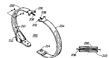
FIGS. 3A and 3B show the general construction of a
wristband loop antenna for the preferred embodiment of the
present invention. As shown in FIG. 3A, the wristband loop
antenna 200 includes two non-stretchable, but flexible
straps, or wristband sections 202 and 204. The first
wristband section 202 includes a first conductor 206 which
forms a first portion of the loop antenna, while the second
wristband section 204 includes a second conductor 208 and
forms the second portion of the loop antenna. The first
wristband section 202 further includes a series of
regularly spaced apertures 210, such as holes or slots,
linearly disposed along the wristband to provide
ad~ustability.
A standard two piece clasp, used widely in the watch
industry is utillzed ln the constructlon of the preferred
embodlment of the present lnvention. The clasp is auitably
modlfled, ~uch as wlth plating, to minimize corrosion
problems and to maintaln low ohmlc electrlcal contact when
the clasp is ~ecured. Platings, such as selective gold
platlng of the contact surfaces is preferred, although
other platlng techniques may be employed equally as well.
Ad~ustable clasp 212 is slldably positioned along wristband
section 202, and provldos electrical contact to first
conductor 206. Attached to the end of the second wristband
section 204 19 a flxed clasp 214, which couples to one end
of second conductor 208, and together with adjustable clasp
212 provldes the means to both electrlcally complete the
loop antenna, and to mechanically secure the wrlstband 200
- 2004~65
to the wrist. First wristband ~ection 202 and second
wristband section 204 are affixed to the wristworn devlce
by an attachment means, such as rigid mounting brackets
216, which are secured to the device housing by faqteners,
such as screw~ (not shown). Mounting brackets 216 may be
formed from sheet metal, such as stainless steel, or other
suitable material which i3 generally unaffected by contact
with the skin. Stainless steel is advantageous in not
requiring any plating for providing corrosion resistance.
It will be appreciated, the rigid mounting of the wristband
sections is exemplary and that other attachment means, such
a~ the use of watch style spring loaded pins, may be used
a~ well.
In the preferred embodiment of the present invention,
conductor 208 is a flat sheet-metal conductor formed from
half hard beryllium copper material which is 3-4 mils
thick. Other materials such as copper, nickel silver, and
other conductive materials may be used as well. Conductor -
208 is generally continuous through the length of wristband
section 204, coupling on one end to the fixed clasp 214 and
to a receiver input, such as the recelver ground input, at
the device housing. Conductor 208 may be formed in a
manner shown in FIG. 3B to provide positive retention of
the conductor within the body of wristband ~ectlon 204. -
FIG. 3B shows the construction details for the first
wristband section 202. In the preferred embodiment of the
present invention, wristband section 202 is constructed by
laminating conductor 206 and reactance buffer 218, which
wlll be described ln detail shortly, between top 220 and
bottom 222 members whlch are non-stretchable, flexible
materials formed by any number of suitable methods, such as
by in~ection moldlng or dle cuttlng. Any number of
materlals may be used for the top 220 and bottom 222
members, such as a urethane rubber, leather and the like.
The bottom member 222, or the top member 220, may lnclude a
recessed area, such as receqs 224, ln which conductor 206,
reactance bu~fer 218, and mounting bracket 216 are
positioned. Such a recessed area can be formed in the
2004~65
material when the strap i9 molded. As shown in FIG. 3B,
conductor 206 has an bent conductor portion 236 which i3
used to retain the conductor in the rece-qs and prevents the
conductor from pulling out or moving in the finished
wristband section. When it is impractical to provide a
recess, adhesives may be utilized to provide the retention
of the conductor. Depending on the material of the two
members, the two members may be joined by such processes as
chemical bonding, including solvents and adhesives;
mechanical bonding, including thermal, and ultrasonic
bonding; and stitching or adhesive bonding, as in the case
of a leather wristband. Insert molding of complete
wristband sections may also be used, thereby eliminating
many of the secondary wristband assembly operations
described. Conductors 206 and 208 are formed from flat
sheet metal using such methods as stamplng, chemical
etching, or other suitable process.
FIG. 4 shows a diagram of a wrlstband antenna and an
equivalent electrical schematic diagram which is useful in
describing the operation of both the prior art wristband
loop antenna, and the buffered loop antenna of the present
invention. As previously described, the wristband loop
antenna formed by bands A and B are inductive at the
operating frequency, lndlcated schematlcally as L~b-X)~ the
subscrlpt denotlng the plurallty of inductances as the
length of the loop iq ad~usted (x indlcatlng position Tl to
T7 and b lndlcatlng the reference end of the second band as
shown ln FIG. 4). The reslstance assoclated wlth the
conductors 18 shown ~chematlcally as R9. The wristband
loop antenna couples to a receiver input and ground as
shown, and 19 capacitively tuned, the capacitor shown
schematlcally as Co. In the preferred embodlment of the
present lnventlon, capacltor C0 couples between the
recelver input and ground. The voltage delivered from the
loop antenna operatlng ln an electromagnetlc fleld ls shown
schematlcally as the voltage source labeled E.
The operatlng frequency of the antenna may be
determlned by the followlng well known equation.
200~365
Fant = 1 / 2~ ~ L(b-x) CO
From the previous description of FIGS. 2A and 2B, lt was
noted the lnductance at tap Tl, does not equal the
inductance at the other taps. Thu~
L(b-1) ~ L(b-2) ~ - L(b-7)
where ~(b-1), etc. represents the magnitude of the total
inductance measure at each tap position. The total
inductance of the loop antenna is the sum of the inductance -
of band A and band B, corrected for the differential
inductance associated with varying the length of the loop
in the adjustable zone.
It then follows, if CO is kept conqtant, such a when
the capacitor is pretuned at one of the wristband lengths,
then
Fant(b-1) ~ Fant~b-2) ~ Fant(b-7)
which demonstrates, as previously stated, the prior art
wristband loop antenna requires retunlng to eliminate -~
variations in ad~usting the wristband to different wrist
sizes. This problem is substantially mlnimized wlth the
reactance buffer described in FIG. 3B, the operation of
which will be described in detail with FIGS. 5A and SB. In
practice, the reactance buffer of the present invention
provides substantially a constant reactance for each tap
position along the wristband, such that
L(b~ L(b-2) ~ L(b_
which results in
Fant (b-l) ~ Fant (b-2) ~ Fant (b-7)
The reactance buffer for the preferred embodlment of
the present lnvention, by providing a substantially
constant reactance at each tap position, allows the
wristband loop antenna to be tuned only once at any of the
selectable wristband lengths, and thereafter the wristband
loop antenna remains tuned, even when the diameter of the
antenna loop is changed.
FIG. 5A shows a diagram of the physical layout of the
reactance buffer 21a for the preferred embodiment of the -
present invention. An approximate schematic diagram of
reactance buffer 218 i~ shown in FIG. SB. It will be
' -' '" '
,
~00~65
appreciated, that the schematic diagram of FIG. SB ii only
a first order approximation for the reactance buffer, in
that each conductor in the circuit has an associated
inductance value. The schematic diagram of FIG. 5B
represents inductance values associated with horizontal
conductors. While the vertical conductors also have
inductance values associated with them, they are shown
schematically as conductors, or conductive elements. It
will be appreciated, this first order approximation is
sufficient to one of ordinary skill in the art to
understand the operation of the reactance buffer 218 to be
described.
Reactance buffer 218 is an integrated structure, as
shown in FIG. 5A in that the buffer input, the taps, and
the reactance elements are formed from a flat sheet metal
strip. The taps are linearly disposed along the integrated
structure providing buffer outputs to select the wristband
size. The outermost taps, T1 and T7, are spaced a
predetermined length, corresponding to the amount of
wristband size ad~ustment required.
Referring to FIG. SB, first conductor 206 is shown
schematically as inductor L1. Reactance buffer 218 input
is shown generally as conductor 300. Reactance buffer 218
includes a plurality of taps T1-T7 which are used to ad~ust
the length of the wrlstband, or conversely, the diameter of
the wrlstband loop antenna. It will be appreciated, the
number of taps provided for the ad~ustment range is for
example only, and other numbers may be provided when
necessary. Reactance buffer 218 comprises a plurality of
reactance elements, shown schematlcally as inductive
elements, or inductors, L2-~10. The arrangement, i.e.
series/parallel combinations of these reactance elements,
results in a substantially constant reactance when mea~ured
between the buffer input 300 and each of the taps T1-T7.
As shown, each inductive element is ln actuality a
conductor, the value of the inductance being a function of
the geometry of the inductor. Thus, L2 which corresponds
to conductor 304, has a substantially equivalent inductance
200~65
11
value to L3 which corresponds to conductor 306. Inductance
values at other taps are combinations of inductances
corresponding to a number of series and parallel inductors,
as shown.
Table I illustrates the relative performance of the
inductive reactance buffer compared to the prior art loop
antenna design. All measurements are referenced to tap T1,
and includes a conductor length equivalent to that found in ~-
the first antenna portion. The relative length is the
10 additional length of the wristband, as the wristband is ~ -
adjusted from T1 to T7. The inductance change is the
change in inductance value associated with each tap
relative to the inductance reference measure at T1. The
total inductance and change in inductance for the prior art
antenna are tabulated in the last two columns of TabIe I.
As Table I shows, the change in inductance for the prior
art antenna was measure at 59.1 nanohenries, compared to a
maximum change of 4.3 nanohenries. It will be appreciated
that further optimization of the conductor geometries in
the reactance buffer can be made to reduce thls difference.
As shown in FIGS. 3B and SA, reactance buffer 218 may
be advantageously and economically formed from a single
flat sheet metal conductor which has been formed, such as
by die stamping or chemical etching. It will be
appreciated, the conductor pattern shown is, for example,
only, and any number of conductor patterns may be generated
which achieve the qame result, a qubstantially constant
reactance measured between the buffer input and each output
tap. The conductlve pattern may be formed from sheet
metal, such aq copper, beryllium copper and nickel silver.
The material i~ selected to provide the required
flexibility, and to withstand the repeated flexing
a~sociated with wearing the wristband and repeatedly
putting on and removing the wri~tband from the wrist. The
conductor may be plated to enhance the solderability, and
durability of the conductor, with a plating such as a
copper, nickel, tln plating.
:
;''. ',
`~
2~ 4.~5
12
Other materials for forming the reactance buffer may
also be employed, other than described above. One such
material may be a copper foil laminated kapton material,
wherein the reactance buffer pattern is formed using
convention printed circuit etching techniques. Coupling of
the pattern to the tap areas would be the same, or similar
to the stamped metal reactance buffer, such as with rivets.
Alternate construction methods for the reactance
buffer is shown in FIGS. 6A/6B and 7A/7B. The reactance
buffers of FIGS. 6A/6B and 7A/7B utilize a plurallty of
fixed value capacitors to achieve a sub~tantially constant
reactance when the length of the wristband is adjusted. As
shown in FIG. 6A, a portion of conductor 206 is tapped
using conductors 400-412, somewhat in the method of the
prior art. However, unlike the prior conductor 206 i9
coupled to each output tap Tl-T7 through a fixed capacitor
C1-C7. FIG. 6B shown an approximate schematic diagram of
FIG. 6A. In the instance where both inductive and
capacitive elements are utilized in the reactance buffer,
the reactance elements may be considered to include a
plurality of paired inductive and capacitive elements, such
as L11 and C1. Each inductive and capacitive element has
an input and an output, the input of the capacitive element
being coupled to the output of the inductive element, and ~ -
the output of the capacitive element belng coupled to a
tap. The inductive elements are then coupled in series,
resulting in the structure shown in FIG. 6B. The values
for C1-C7 are -qelected to provide a substantially constant
reactance between the input and each output tap, the
magnitude of this capacitance being computed as follows:
2~fLCum + 1/2~fCtap - a constant
where f lq the frequency of operation, LCum is the
cumulatlve inductance a-qqociated with each tap, and Ctap is
the partlcular tap capacitance. Thus, LCum would equal L11
+ L12, and Ctap would be C2 for tap T2. Thus, C1, when
used, would have the smallest capacitance value for
resonating with inductor L11, whereas C7 would have the
largest capacitance value for resonating with the series
,:,
' ' " '
.
X004365
13
combination of L11-L17. ~hile capacltor C1 is shown, it
will be appreciated C1 can be omitted with the buffer
retaining the same electrical characteristics previously
described, in which case C2 would have the smallest
inductance value resonating with 111 and 112.
One construction method for a reactance buffer
utilizing capacitive and inductive elements is shown in
FIG. 7A. A flexible circuit 508, such as a kapton film
with laminated copper foil i~ first etched to provide a
pattern similar to shown in FIG. 6A. Capacitor~ C4-C7,
such as leadless, surface mountable chip capacitors, having
appropriate values are then soldered, such as uslng reflow -
soldering, to attach the capacitors to the conductors. A
molded, or die cut, elastomer or leather band is then
15 assembled enclosing the flexible circuit using one of more -
of the procedures previously described for the inductive
reactance buffer of FIGS. 3A and 3B.
Table II illustrates the relative performance of the
capacitive/inductlve reactance buffer. All measurements
are referenced to tap T1, and includes a conductor length
equlvalent to that found in the first antenna portion. The
relative length is the additional length of the wristband,
as the wristband is ad~usted from T1 to T7. The total
inductance is listed for three tap posltions. Cadded is
the computed capacitance required to resonate the total
inductance at each tap to a predetermined operating
frequency, whlch in the case of thi~ example is 157.7 MHz.
As table II shows, proper selection of fixed value
capacitors at each tap can substantially eliminate any
changeis ln antenna tuning, as the length of the wristband
is changed.
An alternate construction for the capacitive reactance
buffer is shown in FIG. 7B. In thls instance, the
capacitors are formed during the construction of the
wrlstband sectlon 202. As shown in FIG. 7B, one plate of
capacitors C1-C7 is coupled with a contact 500. The size
of the plate 500 is a function of the capacitance required
at each tap, the thickness of dielectric layer 502, and the
. .
:" ,': '
..
200436S
.
14
dielectric con~tant of dlelectrlc layer 502. Computation
of the size of the capacitor plate is well known to one of
ordinary skill in the art. The second plate of each of the
capacito~s Cl-C7 i9 provided by conductor 206. In
practice, capacitor plate/contacts S00 are placed in a
molded wristband half 504. Each capacitor plate/contact
has a different geometry corresponding to the required
capacitance at each tap. Dielectric layer 502 i8
positioned over the contacts, followed by the positioning
of conductor 206. Dielectr~c layer 502 may be molded from
a suitable dielectric, having a recess in which to position
conductor 206. Finally, the top wristband half 510 is
positioned on the stack, and the combination laminated by
one or more appropriate techniques previously described for
the inductive reactance buffer construction.
As shown in FIG. 7B, wrlstband section 204 may be
constructed to provide connectlon to the capacitor/inductor
buffer. In thl~ lnstance, conductor 208 may be formed,
such as by stamping or colning techniques, to form contacts
506 to be plugged lnto capacitor plate/contacts 500. Two
contacts are shown ln this alternate embodiment of the
present lnvention. The two contact arrangement provides
additional strength to the clasp when the clasp ls secured
as well as a more reliable electrical contact. Other
methods of forming the contact on conductor 502 may also be
employed, such a~ by attachlng separate fixed contacts.
As in the case of the lnductlve buffer of FIG. 5A, the
capacitive buffers of FIGS. 7A and 7B may be described as a ~`
flat integrated structure which includes the buffer input,
taps and reactance elements.
While the description of the buffered loop antenna has
been directed primarlly for use in a wristband, it will be
appreciated, the reactance buffer of the present inventlon
can be used in other loop antenna applications as well.
Examples of such applications, include any variable size
loop antenna, either electrically small or electrically
large and having any cross sectlonal configuration, such as
circular, square, rectangular or other. Other applications
:,
Z004365
include such special purpose variable size loop antennas,
such as could be located in belts, rigid bracelets, ankle
straps, and the like.
While specific embodiments of the present invention
5 have been shown and described, further modifications and -
improvements will occur to those skilled in the art. All -
modifications which retain the basic underlying principles
disclosed and claimed herein are within the scope and -
spirit of the present invention.
We claim:
2004365
8~
~ æ~ l Irl 1~
~ H ll N 1~
:i3
. ,_ _ '
~ ~1 ~ ~ .-
~ n 0 0
_ :
~ ~ H
~ I ~ .
~ N ~ ~ ~; :
;~ O r1 r~ N ~ ~ ~ . .
~ _ .~
~i ' '"",''`
'.
r ,~ r
~ _. ~ ~ ~ ' N 0~ '
1~5 ~ ~ rl r~
_ . : '.
a ~ ~ ~
o ~ u~ ~ ~ ~ a~
C~ ~ O O C~
~ 3 ~o~ O `
~ . ~
~I N ~ ~ In ~O
P~
- 200~65
~ . _ ~ ~
Relat lv~
3and ' 8~ ength lnductanc~
Position~L--B (x? -B ~1) L t~-x) C~dd~d Fant
__ _ . , . . _, :
B-1 O mm 142 . 4 nEI O pF 1~7 . 7S MHz
B-29 . 04 nun ___ ___ _~
B-316. 65 mm ___ ___
B-423 . 05 mm 160 .1 nH39 . 8 pF lS7 . 75 MHz
~-~30 . 07 nan ___ ~__ ___ .
~-6 37 . 0~ __............ _~_ ___
B-7 44 . 09 mm201. S nH 17, 2 pF lS7 . 75 MHz
nH - nasloh~nr~
TA8~9 I 1
~g '~ ~''' ' ' ''
' .
,
~6~