Note : Les descriptions sont présentées dans la langue officielle dans laquelle elles ont été soumises.
:
., . ~q~ss~3
::
:;
.. I FIELD OF THE INVENTION
:.,
2 This invention relates generally to a superconductor
;7
wire. More particularly, the invention pertains to a method of
' ~ manufacturing a superconductor wire capable of controlling the
stress exerted on an internal ceramic superconductor
6 ~ilament. This invention is particularly, but not exclusively,
7 useful for manufacturing a winding for a magnet.
9 DISCUSSION OF T~E PRIOR_ART
- 10 It is generally recognized that superconducting materials
,~ 11 offer a great deal of potential in the electrical industry. In
~ 12 a transmission line or a motor, superconducting material is
;~ 13 capable of transferring large amounts of current without
~?. 1~ generating excessive heat losses because of the extremely low
iY 15 resistance of the superconducting material. Obviously, this
,!i 16 highly e~icient method of transferring electricity will result
i~ 17 in great economic and social benefits in the future. It has
~ 18 been suggested that superconducting material may allow motors
;; 19 to be produced which are one-tenth (l/l0) of the normal size.
;y 20 Additionally, it has been speculated that new superconductive
21 data transmission lines could be constructed to carry one
~ ~ 22 Itrillion bits of information per second, which i~ approximately
"; ~ 3'j~o~7 23 l00 times faster than the fiber optic cables which carry many
!;' ~ c~o ~ 24 data transmissions and telephone calls at the present time.
x~3~ Further, and of particular importance to the present invention
~; 26
.,.,, -1-
: ~ - 2 1)0~5~3
'`'i
',`
1 is the potential for the ~se of superconductor wires in magnet
2 windings.
3 In the past, one of the primary limitations on the
4 development of superconductors has been the fact that most
materials are superconductive only at extremely low
6 temperatures. More recently, however, it has been found that
7 certain specialized ceramics exhibit superconductive properties
8 at temperatures above those of traditional superconducting
9 materials. Appropriately, these specialized ceramics or other
suitable fibers are often referred to in the art as "high
11 temperature superconducting materials." These ceramic
12 superconductors exhibit superconductivity characteristics at
13 the temperature of liquid nitrogen, which is a great
14 improvement over traditional superconductors.
One of the difficulties with ceramic superconductors is
16 their inability to be easily bent or flexed into a desired
17 position, such as into a winding for a motor or magnet.
Unfortunately, ceramic superconductor materials lack the
19 ductility of metallic conductors and cannot withstand much
tensile stress when bent. Consequently, ceramic
21 superconductors generally exhibit a brittle characteristic
22 which has required special design considerations.
23 It is known that a ceramic superconductor can be supported
24 on a substrate fiber to enhance the strength of the ceramic and
to help overcome the difficulties associated with its brittle
26 characteristic. To help support the ceramic superconductor, a
.
:
~ Z~5~3
,.,i . .,
,~
1 superconductive wire is constructed in which the ceramic
2 filaments are embedded in a matrix of a supporting material
3 which is more ductile, in an attempt to surmount the
.j 4 brittleness problem. The use of a supporting material,
however, creates its own problems. For example, when the
6 superconductive wire is bent around a drum to form a winding
~ 7 for a magnet, the supporting material may cause additional
- 8 stress to be placed upon the superconductor filaments. This is
q 9 due in part to the fact that the stress exerted on the wire
;~ 10 during bending or shaping is proportional to one-half the depth
or thickness of the filament divided by the radius of the
1 12 bend. Thus, for a given bend radius, increasing the thickness
13 increases the stress, and since the ceramic filaments are
14 embedded in and are bound to the supporting material, the
increased thickness of the wire results in more stress upon the
16 ceramic filaments. It would be an improvement over the prior
~ 17 art if a ceramic superconductor was supported by a surrounding
1 18 matrix material that did not increase stresses exerted on the
19 ceramic filament when being bent or shaped.
l 20 Another problem is encountered when superconductors are
?., ~ 21 used to transmit electrical current. When current passes
~ 22 through a wire, electromagnetic forces are generated within the
~^ 23 material which can place significant stresses on the
24 material. These additional forces created by the current are
virtually unavoidable and must be taken into consideration when
26 designing magnet coils and transmission lines. Thus, a
:
~` -3- `
. .; ,: . ~. ,- : : - : - , ~ ... ... , : -
:. , : . .
.,: . .
zb~5573
...
. ,.
1 superconductive wire already having external stresses placed on
2 it by its supporting material has additional stresses placed on
it by high current passing through it. This can cause the wire
4 to fracture and hence become ineffective as a conductor. Thus,
;~ 5 any reduction in stress exerted on the ceramic superconductor
6 wire would be an improvement over the prior art.
J
~~ 7 In light of the above, an object of the present invention
" l
is to have a superconductive wire which supports the
9 superconducting ceramic filaments and controls the amount of
:'
;, 10 stress placed thereon. A related object of the present
11 invention is to have a bendable superconductive wire which
....
12 minimizes external stresses on the internal superconducting
', .'i
~ 13 ceramic filaments while being bent. Further, an object of the
;~1 14 present invention is to make a winding for a magnet which does
;1 15 not have external stresses exerted on it by its supporting
' 16 material. Yet another object of the present invention is to
~ 17 minimize the stress on a superconductive wire when a large
u 18 current is passed through the wire. Finally, an object of the
!
present invention is to have a superconductive wire which is
;~ 20 relatively easy to manufacture and comparatively cost effective
21 for use in the electrical and magnet industry.
22
23 SUMMARY OF THE INVENTION
24 A preferred embodiment of the superconductor wire of the
present invention comprises a thin-walled tube wound around a
26 drum to transmit electricity for a magnet. Positioned within
~; -4-
~'~J::
q~,
: 20~5S~73
;.
,
~:'"!j 1 the lumen of the tube are superconductor filaments twisted
together into one or more bundles for transmitting electricity
?i from a first end to a second end of the tube. For supporting
~' 4 the plurality of superconducting bundles, the lumen of the tube
ti ~l
is flooded with a solder which is allowed to harden and
surround the bundles~ The solder is heated during the winding
j ~ upon the drum to melt the solder and allow realignment of the
8 superconductor filament bundles within the liquified solder to
~i 9 provide unstressed support for the ceramic material.
~;,,j
In the manufacturing of a winding for a magnet made of the
superconducting wire, superconductor filaments are twisted or
12 wound togethe'r to form one or more bundles or cables. The
;, 13 cables are aligned within the tube and liquified solder is
;~;,;l
!3 14 in~ected into the tube. The tube is allowed to cool to
solidify the solder which supports the cables. When making the
winding, the wire is heated to again melt the solder as the
17 wire is wound onto the drum to create the winding. After the
18 winding has been formed, the solder is once again allowed to
19 solidify in order to provide external support for the
superconductor filament cables contained within the supporting
E 21 material. Liquifying the solder during the bending process
~ uuio8~ 22 allows realignment of the filaments within the solder and
,.,~, ~ ~'~3~ô~^ 23 minimizes the stress on the superconductor filaments.
~ 2 The novel features of this invention, as well as the
i ~x 25 invention itself, both as to its structure and its operation,
`~ 26 will be best understood from the accompanying drawings, taken
.!
-5-
',`~':
.. ~.,. , : - . . . . . . .. . . . .
~ ~ s
l~l ~ l
~` ~00~73
`.;.
.. ~ in conjunction with the accompanying description, in which
i! 2 similar reference characters refer to similar parts, and in
which:
.~
~ 4
s BRIEF DESCRIPTION OF THE DRAWINGS
~il 6 Figure l is a ~ront cross-sectional view of one presently
preferred embodiment of the stress controlling superconductor
8 wire of the present invention showing a plurality of
9 superconductor filament bundles surrounded by a filler that is
contained inside a tube;
.,,:
Figure 2 is a perspective view of a filament bundle with a
:` 12 cross-sectional view thereof;
: :'.
13 Figure 3 is a perspective view of a winding of an
... ~ 14 embodiment of the superconductor wire with a portion shown in
'''`'t 15 cross section;
}6 Figure 4 is a cross-sectional side view of the stress
~ 17 controlling superconductor wire showing only a single bundle
.. 'i! within the wire and only a single filament in the bundle; and
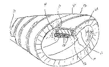
19 Figure 5 is a process diagram showing the method of
manufacturing a stress controlling superconductor wire.
21 :-
8~ 22 DESCRIPTION OF 'i~HE PREFERRED EMBODIMENT
~ 23 Referring initially to Figure l, a front cross-sectional
"~; ~rn~O,O~ 2~ view of the present inven~cion is shown. In Figure l, the
stress controlling superconductor wire, generally designated
:i~ 26 l0, is shown having a surrounding tube 12 with a lumen 14.
. -6-
..,,
5~73
..... .
, ~ ~
, ;..,
;'.
~s~ ~
lthough a cylindrical tube 12 is shown in Figure 1, it is to
~;~ 2 be appreciated that the configuration of tube 12 is not a
3 limitation of the present invention. Indeed, a rectangular
.~ 4 cross section for a structure comparable to tube 12 will be as
,~.. ..
`!`:' 5 efficacious and, depending on the particular application, may
6 be more appropriate. Positioned in tube 12 are bundles 16
7 within lumen 14. In the preferred embodiment, each individual
~,..3
8 bundle 16 comprises a plurality of superconducting ceramic
filaments 18 which are twisted or woven into a cable 52. For
properly positioning and supporting bundles 16 in place within
lumen 14, an electrically and thermally conducting filler 20 is
12 injected into'tube 12 to completely surround the plurality of
~ bundles 16.
~< 14 In Figure 2, a bundle 16 is shown wherein the ceramic
15 filaments 18 are twisted together. As such each bundle 16 is,
~; 16 by itselE, a rope of filaments 18. Several of these ropes or
~ 17 bundles 16 are then subsequently twisted together to form cable
,.,,
``'~! 18 52. Before further discussion of cable 52, however, lt should
' 19 be noted that each element 18 in the bundles 16 can comprise a
metal substrate 54 on which superconductor particles have been
21 sintered to form a ceramic coating 56. In order to help
22 protect ceramic coating 56 and add further electrical
.~O ~^ 23 transmission capacity to filament 18, a silver layer 58 can be
io used to cover ceramic coating 56.
" ~,, 04 3~v~ o~ 24
, ~ ~ 25 Referring now to Figure 3, the orientation of bundles 16
.. ~ 26 inside a rectangular-shaped tube 12 can be more easily
: i'
. ~ .
. -7-
....
,
~9~ ;~ ~)05573
...,~
";''
. ~
g I understood. As can be appreciated from this side cross-
2 sectional view, each bundle 16 is helically disposed within
:3 lumen 14 and extends along the length of tube 12. As shown,
4 tube 12 has a first end 13 and a second end 15. In the
s preferred embodiment, tube 12 can be made of either copper,
6 copper alloy, aluminum or an aluminum alloy. As can be
7 appreciated, filler 20 suspends bundles 16 in place because
8 filler 20 is a solid material in its normal operating state.
~ 9 Preferably, filler 20 is a solder made of a tin-lead alloy. It
;"y
.,,.10 lS to be u~derstood, however, that other solder materials such
ll as alloys containing leadl tin, bismuth, silver, or indium
12 would also be suitable for the present invention~ In any
~1 event, it is important that filler 20 be both thermally and
,`,11~ electrically conducting.
.,,
Still referring to Figures 2 and 3, it can be appreciated
`~i`16 that each bundle 16 is made up of twisted or woven
~` 17 superconductor filaments 18. In the preferred embodiment, as
stated above, each filament 18 comprises a substrate 54 which
' 19 is coated with a superconductor material 56. Superconductor
`~ 20 materials are generally brittle, therefore, filler 20 is
~ .
21 contained within tube 12 to provide stabilizing support against
22 magnetic forces for the brittle superconductor filaments 18.
^ 23 Additionally, filler 20 will provide some degree of lubrication
i~ 24 when it is melted during the winding of cable 52 and tube 12
into their desired configuration.
.,., ~
; 26
,,`.
~ -8-
. .
~:i
~- - ~055~3
.,," ,
;
,.,
,"j,,~
I For purposes of the present invention, tube 12 provides a
,. ...
2 protective casing in which the cable 52 i~ placed. Tube 12
will therefore require some means by which it can be closed
~' 4 around cable 52. Whether this be at joint 60 for tube 12 as
shown in Figure 1 or at the joints 62, 64 for tube 12 shown in
Figure 3, the brazing together at the respective joints can be
7 accomplished with any solder which has a higher melting
! 8 temperature than the solder used for filler 20.
; 9
lo METHOD OF ~SE AND METHOD OF MANUFACTURE
~,, 11 As mentioned above, it is to be understood that ceramic
12 superconductor materials are generally brittle and cannot
:, 13 withstand excessive tensile stresses. In order to manufacture
14 a winding for a magnet or a motor, however, these
superconductor ~ilaments must be bent around a drum.
''! 16 Unfortunately, when the superconductor material is bent,
~ extensive tensile stresses are exerted on the superconductor
;l 18 material filaments. Therefore, when bending the superconductor
~ 19 material, it is preferable that the tensile stresses be
i 20 minimized.
~ 21 Referring now to Figure 4, a bent superconductor wire 10
;;` ~ ~~ 22 is illustrated. In Figure 4, one selected superconductor
~ ~E~^~ 23 filament 18 within a single selected bundle 16 is shown
`~ ~3~oc~ 24 contained within tube 12. Filler material 20 is contained
~ ~ 25 around the entire surface of this bundle 16, as well as all of
1 26 the other bundles 16 not shown in Figure 4, for providing
~ -9-
.,'~
; Z~55~
,,.,
. .
. -.
support when tube 12 is held in a fixed position. Filler
2 material 20 also provides lubrication when the filler 20 is
melted during the bending of tube 12.
It is known that when a fiber or wire is bent, the stress
exerted at the surface of the wire or fiber is maximal and
6 proportional to one-half the depth of the wire or fiber divided
by the radius of the bend. Thus, the stress exerted on tube
: : .
.'.`!`; 8 12, when it is bent, is proportional to one-half the depth 24
ijl divided by the radius 22. Unfortunately, if tube 12 is bent
i.:i'`
, 10 when filler material 20 is in its solid state, the effective
..,.
!`i:.11 half-depth of filament 18 is the same as for tube 12 (i.e. half
I2 of depth 24) and the stress exerted on filament 18 is equiva-
`;:i
;, l3 lent to the stress exerted on tube 12. This only aggravates
14 the already existing stresses on filament 18 which result when
` IS filaments 18 are twisted into bundle 16. Therefore, when
16 filler 20 is in its solid state, any bending of tube 12 exerts
. .,~
~ 17 lncreased stress forces on fllament 18. Obvious ways to lessen
`~ 18 the tensile stress exerted on filament 18 when it is solidly
19 embedded in filler 20 are to increase the radius of bend 22 of
tube 12 or decrease depth 24. Another problem occurs if all
;~ a 21 bundles 16 are aligned in a parallel relationship. To help
~~ 22 overcome this problem, bundles 16 are twisted together in a
~^ 23 helical manner as shown in Figures 3 and 4. If so aligned,
''J.'~ ~ 3~o~ 24 bundles 16 on the outside of the bend will be stretched and the
~ 25 bundles 16 on the inside of the bend will be compressed.
,~;26
,.,ji
` '; ' -10-
... .
:~ `
`:; ~0~.5~7~
.~1 ,
-`~
,:.
I It has been found that in order to lessen these external
forces exerted on ilaments 18 in bundle 16, filler 20 can be
3 liquified when tube 12 is being bent. The resultant forces
:~'3 4 exerted on filament 18 are then only the stress forces exerted
.
.- 5 when fllament 18 has a depth substantially equivalent to depth
.. 6 26. Therefore, external stresses on filament 18 may be reduced
7 by liquifying solder 20 when bending or flexing filament 18.
Moreover, with bundles 16 configured as a helix within tube 12,
9 each bundle 16 is positioned on the outside and inside of the
` 10 bend in tube 12 for substantially equal proportions. This
:
. 11 confiyuration has at least two advantages~ First, this
.~
~ 12 configuration averages the bending strains to substantially
'3 l3 minimize the resultant stresses on the bundles 16. Second, and
14 very importantly for the present invention, the helical
arrangement of filaments 18 minimizes eddy currents within
16 cable 52. With minimal eddy currents, there is less heat
17 generated and low temperatures for more efficient current
,~
;;l 18 transmissions by superconductor ceramic 56 can be realized.
.
:l 19 The method of manufacturing a wire suitable for use as a
winding 42 for a magnet can be readily appreciated by referring
21 to Figure 5. In Figure 5, the method of manufacturing a
22 winding for a magnet is generally designated 28. In method 28,
^ 2~ a bundle 16 of twisted superconductor filaments 18 is disposed
24 within the lumen 14 of tube 12. As can be appreciated, a
bundle 16 of filaments 18 may be unwound from around a bundle
~, Z
`.3 26 spool 30 and tube 12 may be unwound from around tube spool
:',,
':~ -11-
:`~ 2~ 3
,"
.~
,,,,,
:`r, 32. Once the bundles 16 are placed into tube 12 at inserter
..!.:. 2 34, it is necessary to fill lumen 14 of tube 12 with a filler
, 3material 20. As previously discussed, filler 20 is preferably.,,.i.
; 4a solder made of a tin-lead alloy. Filler 20 is heated and
:~, sllquified by heater 36 and is then injected into lumen 14 of
6tube 12 at point 38 so that the lumen 14 is flooded with
7 solder.
~ 8Wire 10 can either be put on an individual spool and
- 9allowed to harden for later use, or can be processed at winding
..,
,~l l0heater 40 to reliquify filler 20 as the tube and its contents,.
, 1lare wound upon a drum 46 to create a winding 42. The melted
solder allows realignment of the superconductor fibers 18
?i' 13within the solder as it is being wound. As is well known in
14 the pertinent art~ the ease with which this realignment process
lS may be accomplished can be enhanced by a slight agitation or
~ 16vibration of tube 12 and its contents during the time it is
;~ 17being bent into the winding 42. The subsequent solidification
,I' 18of the solder after the tube 12 is wound onto drum 46 provides
`"`' 19an unstressed support for the fiber bundles 18 against magnetic
!,``:~ 20forces. A rotater 44 is connected to drum 46 and is rotated in
21 the direction of arrow 48. Winding 42 is made by continuously
~r8~r~ 22~ winding wire 10 around drum 46. Drum 46 can be of several ,a v~ v~
2:~different configurations based on the particular need.
"'' ~ ri r~o~ 2~ While the particular stress controlling superconductor
Zwire as herein shown and disclosed in detail is fully capable
2~ of obtaining the objects and providing the advantages herein
-12-
.~.r
,,!, ,
~ O~
':
.: 1 before stated, it is to be understood that it is merely
.~ 2 illustrative of the presently preferred embodiments of the
.. ;, invention and that no limitations are intended to the details
:~j 4 of construction or design herein shown other than as defined in
:'~i 5 the appended claims.
. ,.j
:i 6
`~i 7
~, 8
:~ 9
~ '' 10
.~, 11
~ 12
.:~ 13
~:1 14
~.~
16
$~ 17
18
~.`! 19
' 20
3 ~ 21
22
24
2~
3, -13-
~: `'`