Note : Les descriptions sont présentées dans la langue officielle dans laquelle elles ont été soumises.
200616~
Description
~APA~ ~ PRES~ SENS~R
~TTH MINI~T7~n DT~T.~CT~TC D~TFT
Technical Field
This invention relates to pressure sensors utilizing
capacitance variations to sense pressure variations, and
more particularly the present invention relates to silicon-
on-silicon pressure sensor designs which employ a silicon
diaphragm, the movement of which due to changes in pressure
varies the capacitance of the sensor and thus provides an
output representative of the applied pressure. Even more
particularly, the present invention relates to silicon-
glass-silicon type sensors or transducers of the "sandwich"
type, in which an extending glass wall supports the
silicon diaphragm above but in juxtaposition to a station-
ary silicon substrate, and still more particularly to the
minimizing of the dielectric drift which occurs in such
sensors.
Background Art
Capacitive pressure sensors are well known and are
employed in capacitance transducers, microphones, rupture
discs, resonators, vibrators and like devices. Many of the
applications for such capacitive pressure sensors require
that the sensors be extremely small, for example, of the
2~)06161.
order of about eight millimeters by eight millimeters (8
mm x ~ mmj or less.
Silicon capacitive pressure transducers are known in
the art. For example, U.S. Patent No. 3,634,727 to Polye
discloses one type in which a pair of centrally apertured,
conductive silicon plates are joined together with a
eutectic metal bond, such that the silicon disc plates flex
with applied pressure, changing the capacitance of the
aperture interstice and providing a capacitive-type signal
manifestation of pressure magnitude. This form of pressure
transducer thus relies on the pressure-induced deflection
of a thin diaphragm, in which the diaphragm deflection as a
function of fluid pressure causes a variation in the
distance between a pair of surfaces which effectively form
the plates of a variable capacitor. Other examples of such
silicon pressure sensors or transducers are included in the
U.S. patents listed below.
In many high accuracy applications typical of those
encountered in aerospace products, long-term drift (for
example 20 years and longer) at an elevatèd temperature
(for example 120~C and higher) of the pressure sensing
element limits the overall achievable system accuracy.
In an exemplary prior art, silicon-glass-silicon
pressure sensor design of the sandwich type (note Figures 1
& 2), used as an exemplary baseline in the disclosure of
the present invention, the dielectric spacer between the
diaphragm and base, particularly in the upwardly extending
wall support area formed by the dielectric layer at the
operative periphery of the sensor, comprises approximately
fifty (50%) percent of the total capacitance of the sensing
element. In the present invention aging or drift in the
electrical properties of this dielectric wall spacer,
typically made of borosilicate glass, located typically at
the periphery of the device, generally identified as "Cp",
has been identified in the invention as being the major
contributing factor to the drift of the sensing element.
~6)06161.
As can be seen in Figures lA & 1, the exemplary prior
art silicon-on-silicon pressure sensor or transducer lG,
which typically i~ generally square in it~ exterior
configuration but often at least generally and preferably
circular or cylindrical in shape for its inner, operative
substructure, generally identified as ''Cc'' in Figure 1,
includes an upper, conductive, square, flexible, appropri-
ately doped, silicon diaphragm 11 and a lower or bottom,
conductive, appropriately doped, silicon base or substrate
12 with a non-conductive dielectric layer and spacer 13
(made of, for example, borosilicate glass) between them, a
closed, evacuated, hermetically sealed, reference cavity,
chamber or interstice 14 being formed between the two
silicon layers 11, 12. The chamber 14 is typically at a
zero vacuum or can be sealed at a higher reference
pressure, at which reference level the diaphragm 11 is
parallel to the silicon substrate 12, with typically a two
micrometer spacing between the two.
It should be understood that the simplified drawings
hereof for practical purposes of illustration are not at
all to relative scale, as the glass wall or spacer 13/16 is
only typically nine micrometers high, in contrast to the
thicknesses of the silicon layers 11 & 12, which typically
are eight thousandths (0.008") of an inch and fifty
thousandths (0.050") inches thick, respectively, for an
exemplary fifty (50 psi) pounds per square inch pressure
measuring unit.
A centrally located, typically circular pedestal or
mesa 12A extends into the typically generally cylindrical,
closed chamber 14 with a thin, insulating layer of glass
13A (not shown in Fig. lA) covering the top of the mesa.
Due to the thinness of the layer 13A, typically only a half
of a micrometer, which is usually deposited after the
relatively high wall 16 (typically nine micrometers), it
does not substantially contribute to any long term drift
problems of the sensor 10, and its changing characteristics
2~)0616~
over the long term (e.g. 20 years) can be ignored, in so
far as the present inventîon is concerned.
As the externai ambient pressure Oll the outside oE ~he
sensor 10 varies, the diaphragm 11 flexes, causing the
spacing between the silicon layers 11 & 12, serving as
capacitive plates, to change, in turn changing the capaci-
tance of the sensor. This change in capacitance as a
result of a change in the exterior pressure on the exterior
surface or upper-side 17 of the diaphragm 11 is used as a
measure of the pressure and its changes.
Conductors or electrodes 18A & 18B (not illustrated in
Figure 1 for simplicity purposes) to the silicon layers 11
& 12 are included for connecting the transducer or sensor
10 into an appropriate circuit, many of which are known to
the art, which measures its changing capacitance as a
function of the pressure. The varying pressure on the
exterior, sensing surface 17 of the elastic silicon
diaphragm 11, causing the diaphragm to flex, changes the
value of the interstitial capacitance between the diaphragm
and the electrode to the lower silicon substrate 12, which
transduces the applied pressure to a measurable electronic
signal. Typically, as noted above, there is about an
exemplary two micrometer gap between the inner, lower,
underside surface of the diaphragm 11 and the top or
upper-side of the mesa 12A, when the sensor is at its zero
or reference pressure, to allow room for the diaphragm to
flex inwardly toward the mesa 12A, as the pressure
increases.
Critical stress region(s) 15 occur(s) at the inner,
edge interface between the flexible silicon diaphragm 11
and the wall(s) formed by the vertically extended,
peripheral portions 16 of the dielectric spacer 13, due to
the flexing movement of the diaphragm about the region(s),
as the ambient or sensed pressure changes. The wall(s) 16
might typically have a horizontal, lateral or radial
thickness of, for example, thirty-six thousandths (0.036")
X00616~
of an inch with a height of, for example, nine (9)
micrometers, while the separately applied, insuiating, mesa
layer of gla~s is onl~ about a half a micron~e~er thick.
The mesa 12A extends up from the main surface of the
silicon substrate 12 an exemplary six and a half micro-
meters, while having an exemplary diameter of one hundred
and fifty thousandths (0.150") of an inch.
The silicon diaphragm 11 and the silicon base 12 may
typically be square [with corners removed for the purpose
of providing access for electrical contacts to the
layer(s), as illustrated], having a horizontal length of an
exemplary two hundred and sixty thousandths (0.260") of an
inch on an edge, while the spacer wall 16 can have an inner
diameter of an exemplary one hundred and ninety thousandths
(0.190") of an inch. The outer, side surface of the wall
spacer 16 can either follow the basic square configuration
of the silicon layers or having an outer circular configur-
ation.
As can be seen in Figure lA, a transition piece 18 is
bonded through an exemplary glass layer 20 to the upper,
exterior surface 17 of the diaphragm 11 and includes a
pressure port 19, through which the pressure to be sensed
is communicated to the diaphragm. In turn the sensor 10 is
appropriately mounted for use in the desired application.
2S These packaging aspects form no part of the present
invention.
An exemplary, prior art, three plate, silicon-glass-
silicon (SGS) device is particularly described in assig-
nee's U.S. Patent 4,467,394 of Grantham & Swindal. Due to
the relative sizes and electrical characteristics of the
three plates, the dielectric wall spacer 16 at the
peripheral, outer, peripheral regions of the device can
account for approximately fifty (50~) percent of the total
capacitance of such a prior art sensor, that is, about one
(1) part in two (2). This peripheral capacitance is
2~)06161
considered parasitic and undesired, as it is pressure
insensitive.
With ~he structural designs of the present invention,
the contribution of the capacitance " ~" of the peripheral,
supporting, dielectric spacer wall to the overall capaci-
tance of the sensor is reduced, for the baseline example,
from about one (1) part in two (2) of the prior art down
to, for example, a maximum of about one (1) part in eight
(8) with a minimum of about one (1) part in ten (10) in the
invention; that is, from about fifty (50%) percent in the
prior art down to, for example, about sixteen (16~) percent
to about ten (10%) percent, or lower, in the invention.
Accordingly, the overall sensor element drift rate is
reduced by a commensurate amount.
Other prior art approaches may have achieved more
favorable ratios than one (1) part in two (2) by the
introduction of complex lead-throughs or by the substitu-
tion of an insulating structure for the silicon base of the
existing design. However, these approaches are either more
costly, because of the complexity they introduce, or they
compromise the sensing element performance because of the
gross introduction of dissimilar materials having expansion
coefficients which do not ideally match.
A further approach is that of U.S. Patent 4,597,027 of
Lehto (issued 06/24/86), which includes recessing the
dielectric layer down into the silicon substrate, so that
it does not extend above the upper plane of the silicon
substrate and no longer serves as a wall spacer, generates
a number of other problems, including diminished precision,
which makes its approach somewhat undesirable. This
approach also requires that the peripheral edges of the
diaphragm be extended down to, in essence, provide the wall
spacing function of the glass wall spacer 16 of Figures 1-4
hereof, which approach, inter alia, causes problems with
respect to the flexing of the diaphragm. In contrast the
diaphragm 11 of the SGS "sandwich" sensor combination of
6161
the invention can be, and preferably is, flat, that is, it
is uniform in thickness across its laterai ex~ent, exoept
for the po~sibility of providing an indentation of small
width for a diaphragm hinge, as discussed in the co-pending
application entitled "Capacitive Pressurë Sensor With
Hinged Silicon Diaphragm" (R-3288hs-ed) referred to above.
Some exemplary prior art patents in the field of
capacitive pressure sensors or transducers, owned by the
assignee hereof, are listed below:
10 Patent No. Title ~Iv~uLx Issue Date
4,530,029 Capacitive P~e~wre C.D. Beri~A;n 07/16/85
Sensor With Low Para-
sitic Capacitance
4,517,622 Capacitive PnY~Lre B. Male 05/14/85
Tra~ ~Pr Sig ~
Conditioning Circuit
4,513,348 Low Parasitic D.H. Grantham 04/23/85
Capacitance Pn#~e
Tr~n~r and Etch
Stcp Methcd
4,467,394 Three Plate Silicon- D.H. Grantham 08/2V84
Glass-Silicon J.L. Swin~
Capacitive PnY~L~e
Tra~l~r
25 4,463,336 Ultra'~n Micnx~ec- J.F. Black 07/3V84
tronic Pn~Lre T.W. Gru~Xi
Sensors A.J. DeMaria
4,415,948 Ele~Lw ~ic Bonded, D.H. Cnu~ham 11/15/83
Silioon Capacitive J.L. Swin~
PnY~Lre T ~ x~l~Pr
4,405,970 Silicon-Glass-Silicon J.L. Swindal 09/20/83
Capacitive Pn~Lre D.H. G~IU~m
~u~Pr
Disclosure of Invention
Thus, in the present invention aging or drift in the
electrical properties of the spacer in the silicon-on-
silicon structure in pressure sensors has been identified
as being the major contributing factor to the drift of the
Z0~616~
sensing or transducer element. With the structural
designs me~hod approaches of the present inven~io~ he
contribution of the capacitance of the peripheral,
dielectric wall spacer to the overall capacitance of the
sensor is substantially reduced down to, for example, a
maximum of about one (1) part in four (4) or five (5)
parts of the total sensor capacitance, and more typically
one (1) part in eight (8) or about one (1) part in ten (10)
or lower; that is, down to, a maximum of about twenty-to-
twenty-five (20-25%) percent, and typically, for example,
down to about sixteen (16%) percent or about ten (10%) or
lower. As a result, the overall sensor element drift rate
is unexpectedly reduced by a commensurate amount.
This disclosure of the invention provides three
illustrated, exemplary approaches (as illustrated in
Figures 2-4), namely, etching the outer edges of the
dielectric wall spacer layer, making the wall(s) it forms
thinner in its horizontal or lateral dimension (Fig. 2);
and/or reducing the horizontal or lateral thickness or
length of the effective peripheral, lower edge(s) of the
silicon diaphragm, where it interfaces in contact with the
wall(s) formed by the dielectric wall support(s) (Fig. 3);
and/or reducing the horizontal thickness or vertical height
of the effective peripheral, upper edge(s) of the silicon
2S base or substrate where it interfaces with the wall(s)
formed by the dielectric wall support(s) (Fig. 4).
These approaches are all relatively inexpensive and
simple, and are easily incorporated in the manufacturing
processes, yet they produce the unobvious and unexpected
result of minimizing the long term drift of the sensor.
These approaches also avoid, for example, any gross
introduction of dissimilar materials having expansion
coefficients which do not ideally match, and yet minimizes
the dielectric drift of the device.
-- 9 --
~ O ~
Additional advantages of the preferred
structures of the present invention are:
1) a longer surface path for any
electrical leakage from one silicon layer to the
other across the surface of the dielectric spacer
wall, i.e., from an exemplary nine (9) microns to
typically about six hundred and fifty (650) microns,
namely by a factor of about seventy (70) or more;
and
2) as a consequence of the reduced,
overall sensing element capacitance, a sensitivity
increase is achieved with devices having similar
diaphragm thicknesses.
In accordance with a particular embodiment
of the invention there is provided a capacitive
- sensor of the silicon-dielectric-silicon type used
to sense physical changes, such as, for example,
pressure changes, comprising:
a conductive silicon substrate;
a conductive, elastic, flexible silicon
diaphragm having an exterior side, said diaphragm
being capable of flexing movement due to physical
changes being sensed; and
a non-conductive, dielectric wall spacer
layer between said silicon substrate and said
silicon diaphragm, said layer providing peripheral
wall(s) extending substantially above said silicon
substrate and joining said silicon substrate and
said silicon diaphragm together; and evacuated,
closed, hermetically sealed chamber being formed
between said silicon substrate and said silicon
diaphragm and being closed off at the sides above
said substrate by said wall(s) formed by said
dielectric layer between said silicon substrate and
said silicon diaphragm; the flexing movement of said
silicon diaphragm due to the physical changes being
- 9a -
2 ~
sensed causing the capacitance of the sensor to
vary; .the capacitance contribution of said
dielectric layer to the total capacitance of the
sensor being no more than about twenty-to-twenty-
five percent of the total capacitance of the sensor.
From a different aspect, and in accordance
with the invention there is provided a method of
minimizing the dielectric drift of a capacitive,
silicon-dielectric-silicon sensor used to sense
physical changes, such as, for example, pressure
changes, which sensor includes:
a conductive silicon substrate;
a conductive, elastic, flexible, silicon
diaphragm having an exterior side, said diaphragm
being capable of flexing movement due to the
physical changes being sensedi and
a non-conductive, dielectric wall spacer
layer between said silicon substrate and said
silicon diaphragm, said layer providing peripheral
wall(s) extending substantially above said silicon
substrate and joining said silicon substrate and
said silicon diaphragm together; an evacuated,
closed, hermetically sealed chamber being formed
between said silicon substrate and said silicon
diaphragm and being closed off at the sides above
said substrate by said wall(s) formed by said
dielectric layer between said silicon substrate and
said silicon diaphragm; the flexing movement of said
silicon diaphragm due to the physical changes being
sensed causing the capacitance of the sensor to
vary; comprising the following step(s):
limiting the capacitive contribution of
said dielectric wall spacer layer to the total
capacitance of the sensor to no more than about
twenty to twenty-five percent of the total
capacitance of the sensor.
. - 9b -
2 ~ ~ 6 ~ 6 1 ~.
The foregoing and other features and
advantages of the present invention will become more
apparent from the following further description and
drawings, in which drawings like reference numbers
have been used across the figures.
Figure lA is a perspective, partially cut-
away view of the silicon-on-silicon capacitive
pressure sensor of the prior art, which, with the
changes of the invention, also provides the
preferred combination or application of the present
invéntion.
Figure 1 is a side, simplified view of a
silicon-on-silicon capacitive pressure sensor of
Figure lA, but with the pressure port transition
piece removed to better show the parts more relevant
to the present invention, and with the silicon
diaphragm "exploded" up off its support spacer
wall(s). Of course, in its final assembly the
diaphragm is bonded and sealed to its glass support
structure to form with the silicon base a
hermetically sealed chamber.
Figure Z is a side, simplified view,
similar to that of Figure 1, but of a first
embodiment of the silicon-on-silicon capacitive
pressure sensor structure of the present invention
for minimizing the dielectric drift of the sensor,
in which the effective dielectric support wall
2ao6l6~
--10--
thickness has been decreased in its horizontal or lateral
dimension by e~cilil,g away an exterior amour,t or pO~tiOïl.
Fi~ure 3 is a side, simplified v e~, simil~r to that
of Figure 1, but of a second, alternative embodiment of the
silicon-on-silicon capacitive pressure sensor structure of
the present invention for minimizing the dielectric drift
of the sensor, in which the part of the effective periphe-
ral vertical height between the two silicon layers has been
increased by removing a bottom portion of the peripheral
edge of the upper silicon diaphragm.
Figure 4 is a side, simplified view, similar to that
of Figure 1, but of a third, alternative embodiment of the
silicon-on-silicon capacitive pressure sensor structure of
the present invention for minimizing the dielectric drift
of the sensor, in which in combination the effective
peripheral vertical height between the two silicon layers
has been increased by removing an upper portion of the
peripheral edge of the lower, silicon substrate.
Modes for Carrying Out the Invention
Contained in Figures 2, 3 and 4, all of which may have
similar dimensions except as explained below, are three
schematic or simplified representations of improved sensing
element structures designed in accordance with the
principles of the present invention to minimize the
electrical effects of the performance of the dielectrical
spacer on the overall electrical drift characteristics of
the sensing elements. Each of these embodiments use as a
baseline the prior art sensor of Figures lA & 1, in order
to best bring out the differences in approach and structure
of the present invention in contrast to the prior art.
Thus, except as otherwise mentioned with respect to the
changes to the peripheral parts of the sensor involving
directly or indirectly the glass wall spacer 16 discussed
below, the structures may otherwise be and preferably are
substantially the same.
2~ 616~.
With reference to Figure 2, the new structure, having
minimized dielectric drift, is produced by the simple
expedient of etching away the outer, peripheral edge
portion 116A of the glass wall spacer 116 employed in the
baseline design illustrated in Figure 1. Structurally this
design should not, and does not in the example hereof,
materially increase the operating stress levels in the
critical interior glass-silicon diaphragm interface region
115 of the vacuum reference cavity 114 over that of the
baseline, prior art design of Figure 1. However, in
contrast to the relatively large, horizontal, dielectric
wall thickness of thirty-six thousandths (0.036") of an
inch in the prior art structure of Figures lA & 1, the
effective thickness of the wall 116 in the inventive
structure of Figure 2 is only an exemplary ten thousandths
(0.010") of an inch thick, an exemplary thickness of
twenty-six thousandths (0.026") of an inch having been
etched away. As a result of the removal of the peripheral
portion 116A, the peripheral edge of the silicon diaphragm
111 extends out laterally past the outer wall surface 116B
of the spacer wall 116 a significant distance, for example,
twenty-six thousandths (0.026") of an inch.
However, some significant thickness of the wall 116,
of course, must remain to effectively hermetically close
off the sides of the chamber 114 and to have sufficient
width to not cause too high of a stress at the silicon-
glass support interface, as the diaphragm 111 flexes down
about the interface into the chamber under the changing
pressure being sensed and felt at its upper surface 117.
In addition to reducing the effective percentage
capacitance contribution of the peripheral dielectric
spacer 116 to the sensor 100, the structure of Figure 2
also provides more precise control over the overall total
capacitance of the sensing element, since the outer
dielectric edge 116B is defined by photolithograhic
processes, rather than, for example, a saw-cut edge
X~ 161
resulting from the dicing processes, as is the case in the
baseline design of Fig~re~ lA & 1. Another beneEit oE the
photolithographic process is that small crack~, which do
occur in a saw-cut, are eliminated.
Presented in Figures 3 and 4 are further, exemplary
variants of the subject design, which do require additional
processing steps in fabrication but also further reduce the
peripheral glass dielectric contribution to the overall
sensor capacitance, minimizing long term drift, and also
provide a more debris tolerant, outer edge structure.
In the approach of Figure 3 the horizontal thickness
of the effective peripheral, lower edge(s) of the silicon
diaphragm is reduced where it interfaces with the wall(s)
216 formed by the dielectric layer 213; while in the
approach of Figure 4 the horizontal thickness of the effec-
tive peripheral, upper edge(s) of the silicon base or
substrate where it interfaces with the wall(s) formed by
the dielectric layer is reduced.
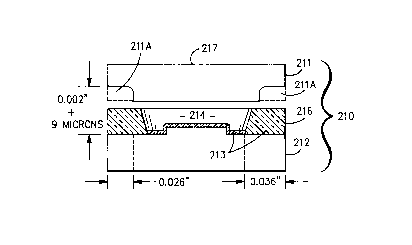
In the sensor structure of Figure 3, the effective,
peripheral edge separation distance between the outer edges
of the silicon layers 211 & 212 has been increased from
only the exemplary nine (9) microns for the baseline
structure of Figure 1 to an exemplary additional two thou-
sandths (0.002") of an inch. Additionally, the interfacing
silicon-to-glass contact area 218 between the silicon
diaphragm 211 and the dielectric walls 216 has been reduced
from a relatively large thickness of thirty-six thousandths
(0.036") of an inch to an exemplary ten thousandths
(0.010") of an inch, an exemplary twenty-six thousandths
(0.026") gap or peripheral portion 211A having been removed
about the periphery of the sensor 210.
In the approach of Figure 4, the effective peripheral
vertical height between the two silicon layers 311 & 312
has been increased by removing an upper, outer edge portion
312A of the peripheral edge of the lower, silicon substrate
312 to an exemplary depth of fifty micrometers, as opposed
g6161
to the "normal" or prior art spacing of the nine micro-
meters providea by the spacer wall 316. As a resuit or
the removai of the outer edge portion 312A, the silicon
substrate 312 has a peripheral area which is lower than the
more inner portion 312B, which is under the spacer wall
316, which actually supports the diaphragm 311 above the
substrate. This effectively decreases the directly
interfacing area between the diaphragm plate 311 and the
substrate plate 312 which has the dielectric wall layer 316
directly in line between them.
With respect particularly to the illustration of
Figure 4, as noted above, the drawing is not to relative
scale, and, in fact, the removed portion 312A along the
periphery of the silicon base 312 is approximately an
exemplary five and a half (5.5) times greater in thickness
or depth than the height of the wall spacer 316 (an
exemplary fifty vs. nine micrometers), which is deposited
on the silicon substrate 312 after the peripheral portion
312A has been removed.
Devices having the design of Figure 4 have been
fabricated and tested. Overall dielectric reductions by a
factor of eight (8) have been achieved with concomitant
reductions in sensing element drift observed experiment-
ally.
A further approach under the invention would be to
increase the height of the support wall spacer with a
concomitant increase of the protrusion of the mesa into
the reference cavity chamber, while still maintaining the
exemplary two micrometer spacing at the zero or pressure
reference level between the underside of the diaphragm and
the upper-side of the substrate.
The three exemplary approaches of Figures 2-4, as well
as other approaches to the problem, can be alternatively or
conjunctive used, as desired. As is well known, a number
of factors influence the peripheral capacitance produced in
conjunction with the glass spacer wall 16-316, including
h ~ ~r ~
--14 ~
the effective separation distances between the capacitor
plates, namely the silicon layers, tne permativity or the
wall spacer material, tne horizontal, interfacing or
juxtapositioned effective capacitive plate area(s)
involved, etc.
As noted above, for disclosure purposes, the three
exemplary embodiments of the invention (Figs. 2-4) used as
a starting baseline the prior art embodiment of Figures lA
& 1. However, in regular commercial use, the sensors
having minimized dielectric drift in accordance with the
principles of the present invention would be designed from
the beginning with the desire of minimizing within
functional reason the capacitance contribution of the
dielectric spacer wall to the total capacitance of the
sensor, with the dielectric layer's contribution being no
more than about twenty to twenty-five percent of the total
and more preferably being about sixteen percent or less of
the total. When so designed from the beginning, its
appearance may be substantially different than that
illustrated in Figures 2-4. Additionally, as known to
those of ordinary skill, other approaches to minimizing the
dielectric layer's contribution to the total capacitance of
the sensor are also possible, the three detailed above
being merely exemplary.
Additionally, it should be understood that in using
the terms "above" or "below" or vertically or horizontally,
these terms are being used in an exemplary relative sense,
as presented in the drawings hereof. Thus, for example, in
a particular application the silicon substrate could in
fact, of course, be below the diaphragm and, rather than
the silicon layers being horizontally disposed with the
wall spacer being vertical, the silicon layers could be
vertically disposed or disposed at an acute angle to the
horizontal, with the dielectric layer appropriately
positioned relative to them.
~/B~4~
~,.. . ~ .
200616~
-15-
Although this invention has been shown and described
wit~ respect to detailed, exemplary embodiments thereof, it
should be understood by those skilled in the art that
various changes in form, detail, methodology and/or
approach may be made without departing from the spirit and
scope of this invention.
Having thus described at least one exemplary embodi-
ment of the invention, that which is new and desired to be
secured by Letters Patent is claimed below.