Note : Les descriptions sont présentées dans la langue officielle dans laquelle elles ont été soumises.
2 ~
:
1 72434-105
MULTIPROCESSOR CONTROLI.~R HAVING SHA~RED CONTROL
STOR~
Cross~Reference to Related Patent: and Patent Applicatlon
The followlng United St;ates patent and Canadian patent
appllcation whlch are asslgned to the same asslgnee as the instant
application contaln related sub~ect matter.
Tltle Invent~ors Patent No./Serlal No.
Perlpheral Controller Edward F. Getson, Jr. USP4,888,727
With Paged Data John W. Bradley &
, Buffer Management Joseph P. Gardner
il Alfred F. Votolato
'
Method and AppQratus George J. Barlow SN2,007,376
For Limltlng The John W. Bradley & .
Utilization Of An Edward F. Getson, Jr.
Asynchronous Bus Wlth
Dlstrlbuted Controlled
~ 20 Access : :
'~ Back~round Of The Inventlon
~ Field Of Use
~ ,.
The present lnvention relates generally to data
processing systlems. More speciflcally, the present lnvention ~. ~
relates to peripheral controllers for controlllng data transfers ~;
¦ between data processing systems and perlpheral devlces.
;2f)~7(~04
.
,
Prior Art
Most modern data processin~ systems perform
both input and output operations such as reading
from a keyboard or sending data to a line printer.
05 For purposes of efficiency and division of labor,
input and output operations to peripherals in such
data processing systems are usually controlled by
peripheral controllers. The general scheme is that
` these controllers act as intermediaries between the
system bus and the peripheral devices.
Peripheral device controllers have been
increasingly required to simultaneously handle I/O
transactions from a large number of different
peripheral devices. Each of these peripheral
devices may have significantly different operating
characteristics. Hence, in order to enable the
, controllers to handle the differing operating
characteristics of the large number of peripheral
~` devices, peripheral device controllers now employ
microprocessors with mioroprograms tailored to the
requirements of the different devices.
Summary~_f the Invention
In a preferred embodiment of the present
invention a peripheral controller has at least one
data buffer for temporarily storing data transfers
. bstween a system bus and peripheral devices. It
also ha~s two microprocessors. The first micro-
processor controls data transfers between the system
bus and the data buffer, whereas the second micro-
processor controls the data transfers between the
data buffer and the perlpheral ùevices. In
" ~
2~7~
3 7~434-105
addition, a common control store is connected to the two
microprocessors. The control store contains first and second
sequences of microinstructions which control operation of the two
microprocessors.
A test microinstruction is stored in ~he control store
in the preferred embodiment. This test instruction directs each
of the microprocessors to the beginning of its sequence of
microinstructions when the system is powered up.
The controller has clocking circuitry which generates a
clock signal divided into cycles. This clock signal is used in
controlling operation of the microprocessors. Each microprocessor
is assigned a portion of a cycle during which lt may exclusively
access the control store. In the preferred embodiment, the
clocking circuitry also controls the microprocessor's access to a
scratch pad memory which is used for interprocessor communicatlon.
The clocking circuitry also plays a role in controlling seizure of
the data buffer in the preferred embodiment. Each microprocessor
is assigned a portion of a cycle in which it may excluslvely `
access the scratch pad memory and a portion in which it may seize
the data buffer. The portions may or may not be the same portion
assigned to tha~ microprocessor for addressing the control store.
In accordance with the present invention there is
provided a controller for controlling data transfers between a
data processing system bus and peripheral devices, comprising: ~
a. at least one data buffer for temporarily storing data as it ~`
passes between the data processing system bus and the
peripheral devices;
b. a first microprocessor for controlling data transfers between
~7~
3a 72434-105
the data processing system bus and the data buffer;
c. a second microprocessor in communication with th~ first
microprocessor for controllir~g data transfers between the
data buffer and the peripheral devices;
d. a control tore connected to both microprocessors for storing
microinstructions that control operation of the respective
microprocessors; and
e. a timing means which produces a clock signal divided into
i cycles whereln each microprocessor is assigned a portion of a
cycle during which it may exclusively access the control
store.
In accordance with the present invention there is also
provided a method of synchronizing elements of a controller which
controls data transfers between a data processlng system bus and
peripheral devices, comprising,
a. dividtng time into cycles;
b. at the start of a first portion of a cycle, performing an
I lnstructlon fetch by a first microprocessor from a control
store;
c. during said ~irst portion of said cycle,
beginnlng execution of the microinstruction fetched by
the first microprocessor; and
completing execution of a microinstruction previousIy
fetched by a second microprocessor;
d. at the start of a second portion of said cycle, performing an
instruction fetch by a second microprocessor from a control
store r
.~
,.
3b 72434-105
e. during said second portion of said cycle,
beginning execution of t;he microinstruction fetched by
the second microprocessor; and
completing execution of the microinstruction fetched by
the first mlcroprocessor; and
f. repeating the above steps b through e.
In accordance with the present invention there is also
provided a controller for transferring data between first and
second units coupled thereto, wherein said controller includes
first and second processors, ~aid first processor controlling the
transfer of data with respect to said flrst unit and said second
processor controlling the transfer of data with respect to said
second unit; said controller being characterized by comprising:
a timing member for generating a cyclical clock signal, the
; cycles of said clock signal comprising first and second half-
cycles of substantially equal duration, and for applying said
clock signal to said first and second processors;
a control store coupled to both of said processors, said
control store holding a first set o~ microinstructions for -
controlling said first processor and a second set of
microinstructions for controlling said second processor, each of
said sets being unique for controlling the particular functions to
be performed by the respective processor;
said first processor being synchronized by said first half~
cycles of said c:Lock signal to access said control store to obtaln
microinstructions therefrom during said first half-cycles; and
said second processor being synchronized by said second half-
cycles of said clock signal to access said control store ~o obtain
2 0 ~
3c 7Z434-105
`, microinstructions therefrom during said second half-cycles.
Brief Description of the Drawinqs
The foregoing and other objects~ features and advantages
l of the invention will be apparent from the following more
particular descrlption of the invention, as illustrated in the
accompanying
' .
7~
--4--
~ .
'
drawings in which like reference numerals refer to
; the same elements.
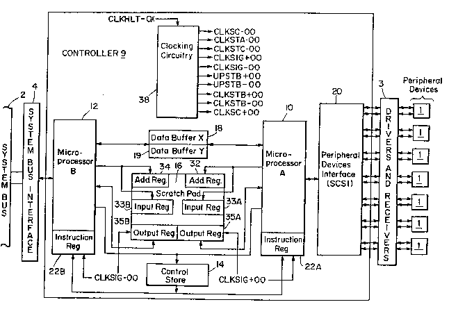
Figure 1 is a block diagram of the controller.
Figure 2 shows in greater detail portions of
05 the controller of Fig. 1.
Figure 3 shows in greater detail the clocking
circuitry of the controller of Fig. 1.
Figure 4 shows in greater detail the memory
used for interprocessor communication.
Figure 5 shows the clock signals generated by
the clocking circuitry and timing of operations of
the microprocessors.
Figure 6 is a timing diagram used to explain
the initialization sequence.
Pigure 7 shows the organization of the control
store and is used in explaininy the initialization
sequence.
Detailed Description of the Preferred Embodiment
In the preferred embodiment of the invention
illustrated in Fig. 1, a controller 9 controls the
data transfers between the system bus 2 and the
peripheral devices 1. The controller 9 can control
data transfers from a multitude of different types
of peripheral devices 1 and i8 designed to control
up to sixteen data channels. Two of the channels
are not used by peripherals, thus, the controller
can simultaneously c~ntrol up to fourteen peripheral
devices.
The basic elements of the controller include
two microprocessors lO and 12. They are connected
- Zf)~3700~
,`
to allow communication with each other and to allow
sharing of a control store 14. The control store 14
is comprised of a Random Acce6s Memory (RAM) such as
the Hitachi 6789. They also are connected t~ allow
o5 sharing of a scratch pad memory 16 as well as to
, allow sharing of data buffers 1~X and 18Y. In the
preferred embodiment, the scratch pad memory 16 is
comprised of RAMs such as the Hitachi 6789 and the
6267P-45, and the data buffer is a RAM such as the
Hitachi 6287. Microprocessor 12, designated as
microprocessor B, controls data transfers between
the ~ystem bus 2 and the data buffer 18X and 18Y,
whereas microprocessor 10, designated as
microprocessor A, controls data transfers between
the data buffer 18X and 18Y and the peripheral
devices 1. The operation of these microprocessors
10 and 12 is governed by the clocking circuitry 38.
The details of the clocking circuitry 38 will be ;
discussed below.
The controller is adaptable to different system
buses and different peripheral devices. To adapt to
a change in system buses or peripheral devices, new
firmware must be loaded into the control store 14.
Interfaced between microprocessor B and the peri-
pheral devices 1 is a peripheral devices interface
20 which meets the Small Computer System Interface
(SCSI~ specification, (ANSI SPEC. X3.131). In the
preferred embodiment, this interface 20 is a Western
Digital 3392 SCSI controller chip. The peripheral
devices interface 20 performs command, message,
data, and status transfer functions. Connected to
the peripheral devices interface 20 are a series o~
- 2~7~
6 72434-105
drivers and recelvers 3 whlch send and recelve lnformatlon to and
from the perlpheral devices 1. An lnter~ace 4 is also provlded to
interface the system bus 3 with the controller. The lnterface 4
ls more fully descrlbed ln the above-mentloned Barlow et al.
Canadlan appllcatlon.
The present invent~on need not be llmited to two
mlcroprocessor~. More than two may be used, but there must be at
least two. U80 of more than two microprocessors would, however,
require alterlng the synchronlzatlon method.
The elements of rnicroprocessor A, are shown ln more
detall in Figure 2. These elements lnclude an lnstruction
register 22A for receivlng lncoming microlnstructlons from the
control store 14 and decoding circuitry 28A for decoding the
incoming microlnstructions. Decoder units such as Texas
Instruments 14S138 and 74S139 are used. There is, likewlse,
wlthin microprocessor A a sequencer 24A. In the preferred
embodiment, the sequencer 24A ls an Advanced Mlcro Devlce
AMD2910A. The sequencer 24A controls the sequence of execution of -~
mlcroinstructlons. Also included withln mlcroprocessor ls an ALU
unit 31A for performing calculatlons as dlctated by the lncoming
microinstructlons. The ALU unlt 31A has output reglsters llA for
storing its output until th~ output is needed. Microprocessor B ; ;
i~ slmilarly comprlsed of llke elements referenced by the sufflx B
as ~an be seen in Flgure 2.
Figure 3 ~hows the primary elements of the clocking ~-
circultry 38, and speclflc clock signals from that circuitry are ~;
illustrated ln Flg. 5. The
''-' ~'''
B
~ .
)7~ 4
; -7-
`:
clocking circuitry contains a 20 megahertz clock 91.
The output from this clock 91 is the clock signal
CLKOSC-OO. CLKOSC-OO feeds into an inverter 88 and
a D flip-flop 93. It also is used by other
, 05 components of the controller ~.
CLKOSC-OO feeds into the clock signal of the D
flip-flop 93. Both the set and reset inputs of the
~, flip-flop 93 are tied high. The set and reset
inputs are low active, so the flop is not set or
reset during typical operation. The D input i8 the
complemented output of the flip-flop 93, CKlOMZ-OO.
The noncomplemented output is CKlOMZ~OO.
As mentioned above CLKOSC-OO also goes to an
invertar 88. The output from this inverter 88 is
CLKOSC+oo.
Tha CKlOMZ~OO output from the D flip-flop 93
fe~ds into another flip-flop 95. This flip-flop 95
is o~ the JK type. The CKlOMZ+OO signal is
complemented and used as a clock signal by the JK
flip~flop 9S. The set and re~et inputs, which are
low aative, are tied high. The K input is likewise
tied high. The J input i5 the signal CL~HLT-OX.
CLKHLT-OX is generated and used only when in test
mode. This signal is used to halt clock operation
and is not used during normal operation. This
flip-~lop provides two outputs: CLKSIG+OO and its
complement CLKSIG-OO. These two signals are the
basic timing signals used by the controller.
' In addition to feeding into the JK flip-flop
95, the CZ IOMZ I OO slgnal feeds into two NAUD gates,
~'
.
~ )7~4
--8--
90 and 92. In the first NAND gate 90, C~lOMZ~00 is
NANDed with CLKSIG+00. The resulting output is
CLKSTA-00 which is used by other components in the
controller. In the other NAND gate 92, CLKSIG-00 is
o5 NANDed with CKlOMZ~00 to produce CLKSTC-00 which is,
likewise, used by other elements of the controller.
The complement of the signal CLKOSC~00, acts as
the clock input for two JK flip-flops, 96 and 102.
The J~ flip-flop 96 has its J,K and set inputs all
tied high. Its reset input is CLKSIG-00. This JK
flip-flop 96 produces two outputs which are used
elsewhere in the controller: Cl.KSTB+00 and its
complement CLKSTB-00. The other JK flip-flop 102 in
which CLKOSC~00 serves as the clock signal also has
its J,K and set inputs tied high. The reset input,
however, i5 different. It is the signal CLKSIG+00.
The two outputs from this JK flip-flop are UPST~00
and UPST~-00.
The siqnals discussed above are all shown
relative to each other in Figure 5. Their role in
controlling operation of the controller will be
discussed in more detail ~elow.
Figure 4 shows the major elements of scratch
pad memory 16. The foremost element is the memory `
unit 30. Other elements include two address
registers 32, 34 which store addresses received from
the ALUs 31A and 31B of the respective micropro~
cessors 10 and 12. The address registers 32 and 34
work in conjunction with a multiplexer 36. The
multiplexer 36 selects an address from one of the
address registers 32 and 34. The data inputs and
data outputs to and from the memory unit 30 are
~ ~0~70V~
g
stored in input registers 33A and 33B and output
registers 35A alld 35B respectively.
The control store 14 contains sets of micro-
instructions for controlling the operation of each
S microprocessor 10 and 12. When one of these
; microinstructions is read out of the control store
14, it is latched into one of the instruction
registers 22A or 22~ at a time discussed below. For
illustrative purposes, suppose that it is clocked
into instruction register 22A. Dif~erent bits of
the microinstruction held by the instruction
register 22 are passed to the decodin~ circultry
28A, ALU 31A, and/or sequencer 24A. Fields of the
microinstruction such as its opcode are decoded by
the decoding circuitry 28.
If the instruction requires an access to
~ scratch pad memory 16, an address in scratch pad
;~ memory 16 is computed by the ALU 3lA. The ALU 3lA
also must calculate an address if access to the data
buffers 18X and 18Y is required. As previously
mentioned, the se~uencer 24A controls the order of
execution of microinstructions by the microprocefi-
sor. It determines the address for the next micro-
instruction to be executed. After being processed
by these components, the microinstruction's execu-
tion is complete, whereupon the next microinstruc-
3 tion's address held in the sequencer 24A is passed
to the control store 14,~and the whole cycle is
' repeated.
The above description of the operation of one
of the microprocessors 10 and 12 views the micro-
processors in isolation. Since both microprocessors
. . ~, :''.
:. ~
.~,.
'7~4
- 1 o -
10 and 12 share the same control store 14 and
scratch pad memory 18, the clocking circuitry
synchronizes both so that each has sufficient access
to these shared r~sources 14 and 18. The present
05 invention allows for such shared access while
eliminating the need for costly and inefficient
hardware to prevent conflict between the
microprocessors.
Figure 5 shows the basic timing scheme utilized
in the preferred embodiment of the pre6ent
invention. For purposes of illustration, it is
helpful to review how the clock signals shown in
Figure 5 are used during operation of the
controller. A good starting point is point 55 at
which a microinstruction is clocked into the
instruction regi~ter 22A o~ microprocessor A. This
is accomplished by using CLKSIG~00 as the clock
signal to the instruction register 22A. As can be
ssen in Figure 1, the mioroinstruction i8 clocked in
at the leading edge of the high portion of
CLKSIG~00. The instruction register 22A is actually
composed of at least three registers 22AA, 22A~ and
22AC (Figure 2). Each of which holds a third of the
microin6truction.
Immediately after being clocked into the
instruction register 22A, the bits of the
microinstruction travel to other elements of the
microprocessor A. ~Hencej during the half of cycle
CL~SIG~00 between points 55 and 62, execution of the
microinstruction begins. Where the bits of the
microinst~uction held by the instruction registers
22AA, 22AB and 22AC travel i6, as previously
.' '" '
Z~07~
-11--
mentioned, determined by the field they represent.
The bits travel to decoding circuitry 28A, ALU 3lA,
and/or sequencer 24A.
Those bits travelling to the decoding circuitry
05 28A must wait until the decoding circuitry 2a i6
enabled before they ara decoded. The decoding
circuitry 2~A is composed of several decoding units
28AA, 28AB, 28AC, 28AD and 28AE, each of which has a
separate clock signal that enables it. Thus, when a
i 10 microinstruction bits are decoded durlng a cycle of
CLKSIG+00 depends on the clock signal for the
particular decoding unit it enters. The decoding
unit 28AA that decodes instructions to seize or
release the data buffer 18 has the complement of
CLRSTC-00 as one of its enable inputs. As a result,
' ~hat decoding unit 28AA can be enabled only during
time period 63. Similarly, the decoding unit 28AB
that decodes commands to write to the data buffer
has the complement of CLKSTA-00 as one of its enable
inputs. It can be enabled only during time period
64. Also limited to a time period in which it can
be enabled is the decoding unit 28AC which decodes
microinstruction to wrlte to the scratch pad memory
16 by microprocessor A. One of its enable inputs is
the complement CLKSTB-00. It can only be enabled
during time period 65. Decoding unit ~8AE, like- `~;~
wise, has the complement CLRSTB-O0 as one of its
enable inputs.
As mentioned above, bits of the microinstruc-
tion enter not only the decoding circuitry 28A, but
also the ALU 3lA. These bits are used in calcula-
tions performed by the ALU 31A. The significance of -~
; ''''.''
Z~)~)7(~
.
-12-
the calculations depends on the microinstruction
that has been clocked into the instruction register
22A. The output from the ALU 3lA is stored in
output registers 1lA. These registers have a clock
05 input which is the signal OClSTB+00. OClSTB+00 is
the AND of the complement of CLKSTB-OO and the
complement of OPCODl-00. OPCOD1 00 is a signal
produced by one of the decoding units 28AD.
There are four types of microinstructions:
set/reset, ALU, test and branch, and branch. The
first two bits of the microin6truction tell which
type of instruction the microinstruction is.
OPCODl-00 is the output that indicates that the
microinstruction is an ALU type microinstruction.
; 15 OPCOD0-00 indicates a branch microinstruction;
OPCOD2-00 indicates a test and branch microinstruc-
tion; and OPCOD3-OO indicates a set/reset instruc-
tion. They are low active. Thus, CLKSTB-O0 must be
low and OPCOD1-00 must be low for OCISTB~00 to be
high.
Also mentioned above was that bits go to the
sequencer 24A. The scquencer 24A, like the
instruction register 22A uses CLKSIG~00 as its clock
signal. At the rising edge of the CLKSIG~O0 signal,
~ields from the ALU 3lA and decoding circuitry 28A
are clocked into sequencer 24A. The output,
however, is not enabled until UPRCEN-OA is high.
UPRCEN-OA is the`outputi from the NAND gate 119
having inputs: CLKSIG-00 and VPRCEN~00 (a test
3~ signal which is tied high during normal operation).
During normal operation UPRCEN-OA is dictated by
CLKSIG-00. Thus, the fields are clocked into
Z~3~70~
.
-13-
sequencer 24A at point 55. Microprocessor B has
corresponding signals UPRCEN~OB and CLKSIG~00.
UPRCEN~OB is tied high during normal operation.
UPRCEN-OB is the output from the NAND gate 118
05 having inputs of CLKSIG+00 and UPRCEN+OB. The
resulting output from sequencer 24A is not valid
until point 62. This ~icroinstruction data is
clocked into the instruction register 22A at point
60.
The address generated by the seq~encer 24A
travels to the control store beginning at point 62.
The address is used to retrieve a microinstruction
from the control store 14 during the half cycle
starting at point 62. The retrieved microinstruc-
tion is not clocked into the instruction register
22A until point 60. By point 60, execution of the
previously fetched microinstruction is complete. At
point 60, the cycle begins àgain for microprocessor
A.
The above discussion illustrates the synchron-
ization involved in the preferred embodiment. At
point 62, microprocessor ~ has a microinstruction
clocked into its instruction register 22B. It
repeats the steps described above for microprocessor
A, but microprocessor B operates a half of a cycle
of CLKSIG+00 out of phase with the operation of ~ '
microprocessor A. The differences,in timing between ''~'
the microprocessors, can be seen by looking at the
clock signals for each. To begin with, the cloc~
signal to microprocessor B's instruction register is
CLKSIG-00. Further, the decoding units utilize a '~
different clocking scheme. The decoding units
responsible for decoding microinstructions that
~ 70~
:.:
-14-
.,
require scratch pad acce~s, 28~C and 2BBE, have the
complement of UPSTB-00 as their clock signal. The
decoding circuitry unit 28BA that decodes micro-
instructions to release or sei~e the data buffers
05 18X and 18Y has the complement of CLKSTA-00 as its
clock signal. Moreover, decoder unit 28BB which
` decodes instructions to write to the data buffer has
the complement of CLKSTC-00 as its clock input.
As a result of these clock signals, the data
; lO buf~er may only be seized or released by
microprocessor a during time period 67 for the cycle
; of CL~SIG-00 between points 58 and 62. Similarly,
writes to scratch pad memory by microprocessor ~ are
limited to time period 66 and writes to the data
buffer are limited to time period 68. This
synchronization scheme allows both microprocessors
10 and 12 to efficiently share scratch pad memory
16, the control store 14, and data buffers 18X and
18Y wlthout conflict.
The sequenoers 24A and 24B of each
' microprocessor 10 and 12 al~o rely on different
clock signals. CLKSIG~00 is the clock signal for
sequencer 24A as already mentioned, whereas
ChKSIG-00 is the clock signal for sequencer 24B.
! 25 Moreover, sequencer 24A relie~ on CLKSIG-00 as its
output enable. Sequencer 24B, on the other hand,
relies on CL~SIG+00 as its output enable.
Having examined where the fields of a
microinstruction travel upon entering the
instruction register 22A, it is necessary to look
further at the outputs from the decoding circuitry
28A. If a microin~truction requ1ring a data buffer
-:
- 1 s - Z(~)7~)0 ~
to be seized or released is decoded, the appropriate
output from the decoding unit is forwarded to the
seizing logic 19 implemented in Programm~ble Array
Logic (PAL). In the preferred embodiment, PAL20R4A
05 and PAL 20L8A chips are used. The seizing logic 19
determines whether a data buffer is seized by one of
the microprocessors 10 and 12. The PAL 19 is
connected to multiplexers 27 and 29. These
; multiplexers are used to select an address from the
address registers 23 and 25. They are clocked by a
signal CLKSIG~ll which is obtained by complementing
CLKSIGtOO through an inverter 120. The data buffers
18X and 18Y, however, are not the central focus of
the present invention. Thus, a more detailed
~l 15 description of the data buf~ers and seiæing logic is
~ presented in the related application Peripheral
j Controller with Paged Data Buffer Management.
If the microinstruction decoded by the decoding
l circul~ry 28A seeks access to scratch pad memory 16,
the appropriate signals ~rom the decoder circuitry
28A are sent to the scratch pad memory 16. Two
signals are especially of interest: SPMIDA-OO and ~;
~' SRIA02-00. The SPMIDA-OO ¢omes from the decoding
! unit 28AC and indicates that an instruction to
increment the address held in the scratch pad
address re~ister 32 is requested. SRIA02-00
indicates that the scratch pad address register 32
is to be, loaded with the AOP field of the
microinstruction. The AOP field consists of the
seventh through tenth bits of the microinstruction.
These two singals are of special interest becau6e
their co=plemonts dre ORed re~ulting in SPMCLKtOO.
'`" .
r
r,.~ 7004
-~6-
SPMCLR~OO is used as the clock input into the
address register 32.
The address to be accessed in the scratch pad
memory 16 is calculated by the ALU 3lA. The
05 calculated address is clocked into the sc~atch pad
address register 32 at the leading edge of the high
portion of the SPMCLK+OO. The address, however,
will not be used until the multiplexer 36 selects
that address register 3~. Which address register it
selects depends on the state of CLKSIG+OO. If
CL~SIG+OO is high, the multiplexer will select
address register 32. On the other hand, if
CLKSIGfOO is low, address register 34 will be
selected. Thus, the multiplexer 36 does not select
until the half cycle following the half cycle in
which the address is loaded into the address
registers 32 and 34. For instance, the address
register 32 would receive an address during the half
cycle between 62 and 60. The memory location within
the memory unit 30 represented by the address
cannot, however, be accessed until the half cycle
immediately following 60. Once selected, the
address in the addres~ register is used to access
the memory unit 30.
All input for tha memory unit 30 is stored in
input registers 33A and 33~. Register 33A stores
input from microprocessor A and 33B stores input
from mi~roprocessor B. The input registers 33A and
33B have clock signals that are always tied high.
Hen~e, their synchronization is controlled by their
output enable. Tbeir output is enablsd by the
complement of SPMWEN-OA and the complement of
;~r).~700s~
-17-
l SPMWEN-OB signals respectively. SPMWEN-OA and
¦ SPMWEN-OB are derived from the multiplexer 121. If
CLKSIG+OO is high and SPMWRT-OA is high, then
SPMWEN-OA is low and enables t:he output from input
05 register 33A. Similarly, if CL~SIG-OO is low and
SPMWRT-OB is high, SPMWEN-OB is low and enables the
output from input register 33B. Output is stored in
the output registers 35A and 35B. 35A storas output
for microp~ocessor A and 35B stores output for
microprocessor B. Output register 35A has CLKSIG+OO
as its clock signal and output register 35B has
; CLKSIG-OO as its clock signal. The two output
registers 35A and 35B are, thus, half a cycle out of
; phase.
The above discussion has focused on
microprocessor A for illustrative purposes. It
should be noted that operation of microprocessor
is similar. The difference between the two
microprocessors 10 and 12 rests with the timing
signals that govern their operation. In most
instances, for every signal mentioned in the
discussion of microprocessor A there is a correspon~
ding signal for microprocessor B. The major cor-
responding signals have bsen discussed above.
The above description of the timing was for
illustrative purposes. Microprocessor A and
microprocessor B could be synchronized opposite the
describbd scheme (l.e., microprocessor A and
microprocessor B could swap times when they perform
i 30 given tasks). Further, if more than two
I microprocessors were used, the timing would have to
be altered. For example, if threu microproces60rs
Z')~37~:)04
:'
-18- ~
.
were used, a cycle could be divided into three
portions with each component ;performing operations
during the respective portion time periods. These
variations are encompassed within the present inven-
05 tion.
In order to utilize the control store 14 of thepresent invention, it must first be prepared for
operation. Preparation involves loading a test
;j microinstruction into an initial location 50 (See
Figure 7) in the control store 14. Also loaded into
the control store 14 are sets of microinstructions
52 and 54 for each microprocessor 10 and 12
respectively. They may be oryanized as 6hown in
~ Figure 7 or in other ways if desired. When the
; 15 microprocessors 10 and 12 begin operation, they are
directed to an initial location 50 where the test
j microinstruction is stored.
! The test microinstruction comprises a test and
branch type microinstruction. The test
microinstruction tests the identity of the
microprocessor that executes it. The test microin-
struction knows the identity of one of the micro-
processors. Suppose, for example, that it knows the
' identity of microprocessor A. It compares he
! 25 identity of the microprocessors executing it with
the known identity. If the identity matches the
known identity, a branch occurs. Hence, micropro- -
cessor ~, whose identity matches the known identity,
branches to the beginning of its set of
microinstructions 52 when executing the test
microinstruction. On the other hand, when
microprocessor B executes the test microinstruction,
,
Z~)7~04
- 19--
the identities would not match so it wo~lld not
branch. The next microinstruction in sequential
order, which is the beginning of microprocessor B's
set of microinstructions 54, would be fetched.
05 The timing of this process is shown in Figure
6. At point 5, the test instruction would be
clocked into microprocessor A. During the half of a
cycle immediately following point 5, execution would
begin on the test instruction. At point 6, the test
microin~truction would be clocked into micro-
processor B. During the half of a cycle immediately
following point 6, microprocessor A would branch.
Microprocessor B would begin executing the test
instruation. At point 7, the first microinstruction
lS Of the set of microinstructions 52 for micro-
processor A would be clocked into microprocessor A.
Processing for microprocessor A would then be as
previously described. Microprocessor B would
complete execution of the test instruction during
the half of a cycle immediately following point 7
and load in the first of its set of microin-
structions 54 at point 8. After point 8, processing
for microprocessor B would be as previou~ly
described.
The present invention offers several advantages
which improve system performance over the prior art.
First, it does not require expensive and burdensome
hardware to synchronize,the microprocessors.
Second, it is more efficient than the prior art
because it shares data buffers, scratch pad memory,
and a control store. There is no need for separate
data buffersJ scratch pad men~ories, and, in
2':~)7~04
~ -20-
:,
, particular, control stores for each microprocessor.
!' Third, because of the synchronization, pseudo or
apparently simultaneous read/write capability is
provided. These are just a few of the advantages.
05 It should be understood that 1:his list of advantages
is not exhaustive.
' While the invention has been particularly shown
and described with reference to a preferred
embodiment thereof, it will be understood by those
5killed in the art that varlous changes in form and
;~ details may be made therein without departing from
the spirit and scope of the invention as defined in
the appended claims.
~.
,, .
,.;