Note : Les descriptions sont présentées dans la langue officielle dans laquelle elles ont été soumises.
NE-245
2~07~2
- 1 -
TlTLE OF THE INVENTION
2"Parallel Mode Adaptive Transversal Equalizer
3For High-Speed Digital Communications System"
4BACKGROUND OF THE INVENTION
5The present invention relates generally to adaptive transversal
- 6equalizers, and more specifically to an adaptive transversal equalizer
7capable of operating at the speed of digital communications systems.
8Transversal equalizers are used for equalization of a digitally
9demodulated signal, and development efforts are being directed to
, 10 digitizing transversal equalizers to meet the recent requirements that
1 1 include compactness, low power consumption and free of adjustments.
12 Prior art all digital transversal equalizers comprise a digital
13 transversal filter and a tap-weight control circuit, or correlator. The
14 digihl transversal filter includes a tapped-delay line to which a digital
~ 15 signal is supplied from the A/D converter of a demodulator. The tapped-
`~ 16 delay line has (2M+1) successive taps (where M is an integer equal to or
17 greater than unity) to which multipliers are respectively connected to
18 multiply the symbols at the taps with respective tap-weight control signals
;~ 19 supplied from the control circuit, the outputs of the multipliers being
~ 20 summed by an adder to produce an equalized signal. The correlator
; 21 includes (2M+1) exclusive OR gates for detecting correlation between the
' 22 data and error components contained in the equalized output, and
2 3 integrators for integrating the outputs of the exclusive OR gates for a
,.; ~ .
2 4 certain symbol interval and averaging the integrated values to produce the
'''.! 2 5 tap-weight control signals to adjust the tap weights at the intervals of the
.:,
2 6 symbols supplied to the hpped-delay line to adaptively equalize the dah
,,.,~.
:`'`'
NE-245 20~7922
- 2 -
signal.
s 2 However, there is an upper limit that is imposed on the maximum
4 3 operffing speed of the correlator and on the maximum operating speed of
4 LSI circuits that comprise the multipliers and adder of the transversal
S filter. Since the recent digital communications system demands ever-
6 increasing speed which is higher than the operating speed of the current
7 LSI circuit, the prior art all digitized transversal equalizer is not capable of
~' 8 meeting the demand of the digihl communications system. Therefore,
9 with the current digital technique, the integrators of such correlators have
10 to be implemented in analog form to meet the high speed requirements of
;: 1 1 the digital communications system.
;.,
12 SUMMARY OF THE INVENTION
13 It is therefore an object of the present invention to provide an adaptive
. .,~ .
14 transversal equalizer which is capable of operating at a speed higher than
1 S the maximum operating speed of LSI chips.
16 In the demodulator of a digihl communications system, a P-channel
17 (in-phase channel) baæband signal and a ~channel (quadrature-channel)
18 baseband signal are derived from a received digitally modulated signal
19 using quadrature demodulation technique and a clock signal synchronized
2 0 with symbols contained in the baseband signals are recovered. P-channel
21 and ~channel analog-to-digital (A/D) converters are provided for
2 2 converting the P-channel and ~channel baseband signals, respectively,
2 3 into P-channel and ~channel digital data streams.
2 4 According to the present invention, the P- and ~channel data streams
2S are decomposed into N sequences (where N is an integer equal to or
2 6 greater than 2) so that they propagate in parallel mode at the speed of LSI
. ~ ,
. - . . ,, . - . -
., . ~
... . ~. .. .. 1
,",, " ~ "
:: :: ,, ... ~ . . . . . .
NE-245 2007922
- 3 -
circuits and are recombined at the outputs.
2 The adaptive transversal equalizer of this invention includes a
3 frequency divider for dividing the frequency of the clock signal by N to
4 produce a sequence of lower-frequency clock pulses, where N is an integer
5 equal to or greater than two. (N-1) P-channel delay circuits are provided
6 for delaying the P-channel digital data stream by one symbol interval to
7 produce (N-1) successively delayed P-channel data streams, and (N-1) ~
8 channel delay circuits are provided for delaying the ~channel digital data
9 stream by one symbol interval to produce (N-1) successively delayed ~
10 channel data streams. N P-channel transversal filters and N ~channel
11 transversal filters are provided, each of which comprises a common
12 tapped-delay line, and a latch having inputs respectively connected to
13 successive taps of the hpped-delay line, the latch being clocked by the
14 output of the frequency divider for sampling and holding symbols at the
15 successive taps of the delay line for a duration of N-symbol intervals. In
16 each transversal filter, there are provided a first group of variable tap-
17 weight multipliers and an adder and a second group of variable hp-
18 weight multipliers and an adder, the inputs of the tap-weight multipliers
19 of each gr~up being coupled respectively to the outputs of the latch and
2 0 their outputs being summed by the adder of the same group to produoe first
21 and second equalized outputs from each transversal filter. The hpped-
2 2 delay line of one of the transversal filters of each channel is connected to2 3 the output of the A/D converter of the same channel, while the hpped-
2 4 delay lines of the other transversal filters of each channel are connected
2 5 respectively to the output of the delay circuits of the same channel. The
26 first equalized outputs of the transversal filters of each channel are
..~
. . .
NE-245
2~7922
--4 --
combined with the second equalized outputs of corresponding transversal
2 filters of the other channel and multiplexed into a P-channel output and a
3 Q-channel output. N pairs of P-channel correlators are associated
-~ 4 respectively with the P-channel transversal filters and N pairs of Q-
channel second correlators are associated respectively with the ~channel
6 transversal filters. One of the correlators of each of the N pairs detects a7 correlation between data and error components of the P-channel output
, 8 for controlling the first variable tapweight multipliers of the associated
9 transversal filter, and the other of the correlators of each of the N pairs
~ 10 detects a correlation between a dah component of one of the P- and Q-
-, 11 channel outputs and an error component of the other channel output for
12 controlling the second variable tapweight multipliers of the associated
;; 13 transversal filter.
14 BRIEF DESCRIPl'ION OF THE DRAWINGS
15 The present invention will be described in further detail with reference
1 6 to the accompanying drawings, in which:
,,.,~
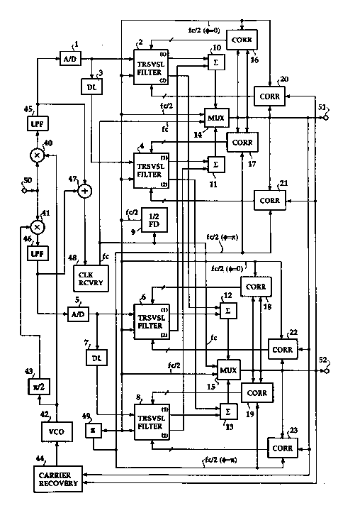
~ 17 Fig. I is a block diagram of an adaptive transversal equalizer of the
! ,j 18 present invention in a two-parallel mode;
19 Flg. 2 is a circuit diagram showing details of the transversal filters 2
20 and40fFig. 1;
` 21 Fig. 3 is a timing diagram useful for describijng the states of symbols
2 2 appearing in Fig. 2; and
23 Figs. 4A and 4B are block diagrams of an adaptive transversal
2 4 equalizer of the invention operating in a thre~parallel mode.
DETAILED DESCRIPIION
26 Referring now to Fig. 1, there is shown an adaptive transversal
.,,
;, . . , , ,
. .
NE-245 2~07~22
-5-
.
equalizer of the present invention for use with a demodulator of a digital
2 communications system. The adaptive transversal equalizer generally
3 comprises three-tapped, two-dimensional transversal filters 2, 4, 6 and 8.
4 As will be described in detail later, each transversal filter is provided with a
5 common tapped delay line having three successive hps, for example, and a
6 pair of latches coupled to the taps of the delay line to apply signals at the
7 taps to multipliers of different sets at one half the rate of the clock pulse
8 recovered by the demodulator where the signals are multiplied by tap
g weight coefficients. The outputs of the multipliers of each set are summed
10 to produoe a pair of equalized signals from each transversal filter.
11 The demodulator is a well-known circuit in which the received signal
12 (be it in PSK or QAM format) is applied through terminal 50 to multipliers,
13 or mixers 40 and 41. A volhge controlled oscillator 42 supplies the in-
14 phase version of a local carrier to mixer 40 to produoe an in-phaæ output
15 as a P-channel digital baæband signal, and a ~c/2 phase shifter 43 supplies
16 the quadrature version of the local carrier to mixer 41 to produce a
17 quadrature output as a Q-channel digihl baæband signal. VCO 42 is
1 8 controlled by a signal which is derived by a carrier recovery circuit 44 of a
19 known design from signals which appear at P-channel and Q-channel
20 output terminals 51 and 52. The outputs of mixers 40 and 41 are
21 respectively passed through low-pass filters 45 and 46 and combined, on
2 2 the one hand, by an adder 0 for coupling to a known clock recovery circuit
2 3 48, and supplied, on the other, to analog-to-digital converters 1 and 5,
2 4 respectively.
25 A/D converter 1 samples the low-pass filtered, multilevel of the P-
26 channel signal and quantizes the samples into a multibit code as a P-
. .
....
. . .
... .. , , . . , . . .. , . , ~. . ..... .
. . . , ~. , .. ;, . ~ ,
... . . ~ . .. . . . .
NE-245 2~0~922
- - 6 -
, . .
channel digital signal. The output of A/D converter 1 is applied to the
2 input of the tapped delay line of transversal filter 2 on the one hand, and
3 passed, on the other, through a one-symbol delay line 3 to the input of the
4 tapped delay line of transversal filter 4.
Referring to Fig. 2, transversal filter 2 comprises a common tapped
6 delay line consisting of unit delay elements, or shift registers 31 and 32
7 successively connected to the output of A/D converter 1 to define an odd
8 number of taps, say, three taps. These taps are connected respectively to
9 input terminals a, b and c of a latch 34. Output terminals d, e and f of the
0 latch 34, which correspond to the input terminals a, b and c, are connected
1 respectively to tap weight multipliers 35 to which tap weight control
, . .
l 2 signals are respectively supplied from an cross-correlator 16. The outputs
l 3 of multipliers 35 are summed in an adder 36 and supplied to an adder 10 as
l 4 a first output of transversal filter 2. Transversal filter 2 further includes a
l 5 similar set of a latch 37, tap-weight multipliers 38 and an adder 39. Latch
.
l 6 37 has its input terminals respectively coupled to the sucoessive hps of thel 7 common delay line and has its output terminals respectively coupled to the
l 8 ta~weight multipliers 38 to which control signals are supplied respectively
l 9 from a cross-correlator 20. The outputs of multipliers 38 are summed by
2 0 adder 39 and fed to an adder 12 as a second output of transversal filter 2.
2 l Latches 34 and 37 are both driven by the lower frequency clock from divide-
2 2 by-two frequency divider 9.
2 3 In like manner, transversal filter 4 is of the same construction to filter 22 4 but it takes its input digihl signal from the output of the one-symbol delay2 S line 3. Transversal filter 4 supplies its first output from its adder 36 to an
2 6 adder 13 and its second output from its adder 39 to an adder 13. The tap
, ,.
",.
. . .
- jrj
;,',~.,'
'- , . ~,, , ~. ' '' ' '
' ~ ' ~ ' .
'',~ . ' , ' " ' '~', ' . : '
NE-245
2~7~2~
- 7-
~, .
weights of the multipliers 35 and 38 of filter 4 are respectively controlled by
2 signals from an cross-correlator 17 and a cross-correlator 21.
3 Returning to Fig. 1, the first output of transversal filter 2 is summed
4 with the second output of transversal filter 6 by the adder 10 and the
second output of transversal filter 2 is summed with the first output of
6 transversal filter 6 by the adder 12. Likewise, the first and second outputs7 of transversal filter 4 are respectively summed with the second output of
8 transversal filter 8 by the adder 11 and the first output of transversal filter-
9 6 by the adder 13.
Stated differently, each of the P- and ~channels of the equalizer has
11 first and second transversal filters. The first output of the first transversal
12 filter of the P-channel is summed with the second output of the first
13 transversal filter of the ~channel, and the second output of the first
14 transversal filter of the P-channel is summed with the first output of the
15 first transversal filter of the ~channel. Likewiæ, the first output of the
16 second transversal filter of the P-channel is summed with the æcond
17 output of the second transversal filter of the Q~channel, and the second
18 output of the æcond transversal filter of the P-channel is summed with the
. .,
~; 1 9 first output of the æcond transversal filter of the ~channel.
,.~
20 On the ~channel side of the adapffve equalizer, transversal filters 6
21 and 8 correspond respectively to transversal filters 2 and 4, respectively.
2 2 Namely, the transversal filter 6 procesæs the output of A/D converter 5
2 3 which samples the low-pass filtered, multilevel of the ~channel signal
24 and quantizes the samples into a multibit code as a ~channel digital
2 5 signal. The output of A/D converter 5 is delayed by a one~nnbol delay line
.
:~ 2 6 7 and supplied to transversal filter 8. The tap weight control signals for
,::.;
."".:.
. ..
..:,
.... , . . ~ , ,~, .. ~ ... , . . -
.~ ~ . - . . . - .
NE-245 2~C79~2
- 8 -
,,
transversal filter 6 are supplied from an cross-correlator 18 and a cross-
2 correlator 22, and those for transversal fUter 8 are supplied from an cross-
3 correlator 19 and a cr~ss-correlator 23.
4 The outputs of P-channel adders 10 and 11 are supplied to a parallel-
S to-serial converter, or multiplexer 14, and the outputs of ~channel adders
6 12 and 13 are coupled to a multiplexer 15. The outputs of multiplexers 14
7 and 15 are connected respectively to the output terminals 51 and 52. The
8 clock pulse recovered by clock recovery circuit 48 is at a frequency fc which9 is divided by a divide-by-2 frequency divider 9 to produce a lower
. .
10 frequency clock at fc/2 which is supplied to the latches of all transversal
11 fUters 2, 4, 6 and 8. Multiplexers 14 and 15 are supplied with the lower-
12 frequency clock in order to receive output signals from the associated
13 adders and are supplied with the higher-frequency clock to combine them
14 into a single bit stream.
15 A phase shifter 49 is connected to the output of divide-by-2 frequency
1 6 divider 9 to delay the lower-frequency dock by ~c radian so that the delayed
17 lower-frequency clock is opposite in phase to the nondelayed lower-
18 frequency clock. The zero-phase lower-frequen? clock is supplied to the
19 cross-correlators 16,18, 20 and 22, and the ~-phase lower-frequency clock
20 is supplied to the cross-correlators 17,19, 21 and 23, so that P-channel
21 correlators 16, 20 and ~channel correlators 18, 22 operate synchronously
2 2 with desired components of the outputs of transversal fUters 2 and 6, while
23 P-channel correlators 17, 21 and ~channel correlators 19, 23 operate
24 synchronously with desired components of the outputs of transversal
2 S fUters 4 and 6.
2 6 Each of the correlators includes a shift register for delaying the input
r.
.~ i
-
~:.
:;
~, ~ . , .
~ ' ' :~ . : , - . ' ' : '
. ~. ' '' ' " "' ' ' - ~ .. .....
'., ' . . , , : '~
.-,~,. ' ' . ' . :
;
,~",
.. : . . . . .
NE-245 2~7922
~. g
by predetermined symbol intervals and (2M+1) exclusive OR gates coupled
2 to the stages of the shift register. The output of the exclusive OR gates are
3 combined and integrated over a predetermined duration by counters to
4 produoe tap weight control signals.
S Since correlators 16 and 20 are driven by the zero-phase lower-
i 6 frequency clock, cross-correlator 16 detects correlation between data and
7 error components which are both derived through P-channel multiplexer
8 14 and produce tap weight control signals to the multipliers 35 of
9 transversal filter 2 at the rate of lower-frequency clock. Whereas, cross-
l o correlator 20 provides detection of correlation between error components
l l which are derived through P-channel multiplexer 14, on the one hand, and
l 2 data components which are derived through ~channel multiplexer 15, on
l 3 the other, and supplies tap weight control signals to the multipliers 38 of
l 4 transversal filter 2 at the lower-frequency clock timing.
l S Since the dah inputs of transversal fUters 4 and 8 are delayed one-
....
.. 16 symbol interval with respect to those of transversal filters 2 and 6, and
;; l 7 since correlators 17 and 21 are clocked with the ~-phase lower-frequency
,:,.
. l 8 clock, cross-correlator 17 detects correlation between data and error
*.
~. l 9 components which are derived through P-channel multiplexer 14, whereas
. ,~.
20 cross-correlator 21 provides detection of correlation between error
; 2 l components which are derived through P-channel multiplexer 14, on the
22 one hand, and data components which are derived through Q-channel
.
- 2 3 multiplexer 15, on the other.
.. 2 4 It is seen therefore that cross-correlator 18 detects correlation between
2S data and error components which are derived through Q-channel
26 multiplexer 15, whereas cross-correlator 22 detects correlation between
;;..
. .), .
..;~.
., ., .:
. ......... .
. . . , ~ - .~ . ~ . ,
.;. . . .
NE-245 2~7~22
. - 10-
error components which are derived through ~channel multiplexer 15, on
2 the one hand, and data components which are derived through P-channel
3 multiplexer 14, on the other. Likewise, cross-correlator 19 detects
4 correlation between data and error components which are derived Q-
S channel multiplexer 15, whereas cross-correlator 23 provides detection of
6 correlation between error components which are derived through Q-
7 channel multiplexer 15, on the one hand, and data components which are
8 derived through P-channel multiplexer 14, on the other.
9 A timing diagram shown in Fig. 3 illustrates the timing relationships
10 between symbols, or bits appearing at the input digihl data stream
1 supplied to transversal filter 2 or 6 and those appearing in the latch 34 of
12 transversal filters 2, 4, 6 and 8. The input digital data stream supplied to
3 filter 2 or 6 is shown in part (A) of Fig. 3. As shown in part (B) of Fig. 3,
14 because of the one-symbol delay elements 31 and 32, the input symbols
S appear at the successive taps a, b and c of the la*h 34 of filter 2 (or 6) as a
16 series of symbols Do to D8 at tap a, a series of symbols D 1 to D7 at tap b,
17 and a series of symbols D 2 to D6 at tap c. Whereas, in transversal filter 4
18 (or 8), the series of symbols which appear at hps a, b and c are delayed one
19 symbol interval with respect to the corresponding series of transversal
20 filters 2 (or 6) as shown in part (C) of Fig. 3 because of the one-symbol
21 delay by delay line 3 (or 7). Since the latches of all transversal filters are
2 2 driven at one half the rate of the incoming data stream, a series of symbols23 D1,D3, Dsand D7 appear at output terminal d of latch 34 which
.:~
` 2 4 corresponds to tap a, a series of symbols Do, D2, D4 and D6 appear at
~i 2 S output terminal e which corresponds to tap b, and a series of symbols D_1,
26 D1, D3 and Ds appear at output terminal f corresponding to tap c (as
.,~.
.~
...... .
,......................................................................... i
, . . .
..
,. . ~ -
NE-245 2007922
. - 11 -
shown in part (D) of Fig. 3). Whereas, in transversal filter 4 (or 8), the
2 series of symbols which appear at taps d, e and f are delayed one symbol
3 interval with respect to the corresponding series of transversal filters 2 (or
. .
4 6) as shown in part (E) of Fig. 3.
S While mention has been made of an embodiment in which the equalizer
6 is operated in a two-parallel mode by processing each of the channels by
i, 7 two identical transversal filters and driving them at one half the rate of
8 incoming data symbols, the present invention could equally be modified to
9 operate the equalizer at any submultiples of the incoming symbol rate.
-;~ l 0 Figs. 4A and 4B shows an adaptive equalizer which operates in a
l l three-parallel mode by processing each channel with a set of three
l 2 transversal filters. It is seen that the divide-by-two frequency divider 9 of
;i,~ l 3 Fig. 1 is replaced with a divide-by-three frequency divider 60 to produoe a
;.~
:;3 l 4 clock pulse at frequency fc/3, and the 1~ phase shifter 49 is replaced with
; l 5 two 21~;/3 phase shifters 61 and 62. Additionally included are transversal
l 6 filters 63, 64, one-symbol delay lines 65, 66, adders 68, 69 and cross-
~ l 7 correlators 70, 71, 72 and 73.
.` l 8 One-symbol delay lines 66 and 67 are respectively connected from the
l 9 outputs of delay lines 3 and 7 to the data input terminal of transversal
2 0 filters 63 and 64. Adder 68 sums the first output of transversal filter 63 with
2 l the second output of transversal filter 64, and adder 69 sums the first
2 2 output of transversal filter 64 with the second output of transversal filter
23 63. The outputs of adders 68 and 69 are respectively supplied to
24 multiplexers 14 and 15, each of which are clocked with the output of
2 S divide-by-three frequency divider 60 for receiving their inputs and driven
. ~
26 by the higher, original clock frequency for multiplexing the inputs.
~' ,
,
.
NE-245 2~07922
- 12-
1Correlators 17, 20, 19 and 23 are clocked by the 2~/3-phase of the clock
~, 2which is one-third of the clock frequency derived from the clock recovery
~, 3circuit, and correlators 70, 71, 72 and 73 are clocked by the 4~/3-phase of
, .;
4 the 1/3 clock frequency.
; SIn summary, this invention provides an adaptive transversal equalizer
,,
,. 6which comprises a divide-by-N frequency divider (9, 60) for dividing the
. 7frequency of the clock signal from the clock recovery circuit 48 by N to
8produce a sequence of zer~phase lower-frequency clock pulses, where N is
ii 9an integer equal to or greater than two, a phaæ shifter (49; 61, 62) for
1 0 shifting the phaæ of the lower-frequency clock pulæs to produoe (N-1)
1 1 æquences of phaæ-shifted clock pulses; (N-1) P-channel delay circuits (3;
1 2 66) for delaying the P-channel digital dah stream from P-channel A/D
1 3 converter 1 by one symbol interval to produoe (N-1) sucoessively delayed P-
14 channel data streams, and (N-1) ~channel delay circuits (7; 67) for
; ~ 1 S delaying the ~channel digital data stream from ~channel A/D converter
.,
1 6 5 by one symbol interval to produce (N-1) successively delayed ~channel
-: 1 7 data streams; N P-channel transversal fflters (2, 4, 63) and N ~channel
1 8 transversal filters (6, 8, 64). Each of the transversal filters comprises a
1 9 tapped-delay line (31, 32), latch means (34, 37) having inputs respectively
2 0 connected to the successive hps of the tapped-delay line and clocked by the
,.
` : 2 1 output of the frequency divider to hold symbols for a duration of N-symbol
2 2 intervals, first variable tapweight multipliers (35) coupled respectively to
2 3 the outputs of the latch means (34), a first adder (36) for summing the
~; 24 outputs of the first tap-weight multipliers (35) to produce a first equalized
2 5 output, second variable hap-weight multipliers (38) coupled respectively to
2 6 the latch means (37), and a second adder (39) for summing the outputs of
~ ,.".
~!.;., .
' '~'
'~.'~ ;' ' . ' ` ' .
NE-245 2~07922
- 13-
..,
the æcond tap-weight multipliers (37) to produce a æcond equalized
2 output. The tapped-delay line of one of the transversal filters of each of
3 the channels (i.e. filter 2 or 6) is connected to the output of the A/D
4 converter (i.e., 1 or 5) of the same channel, the hpped-delay lines of the
!r S other transversal filters of each of the channels being connected
.. 6 respectively to the output of the delay means of the same channel. N P-
.:,~.,
. 7 channel adders (10, 11, 68) are associated respectively with the N
- 8 transversal filters (2, 4, 63, 6, 8, 64) of each channel, and N Q~channel
9 adders (12, 13, 0) are associated respectively with the N transversal filters
1 0 of each channel so that each of these adders sums the first equalized output
.".
~ 1 1 of the associated transversal filter of one of the channels with the æcond
.- 1 2 equalized output of the associated transversal filter of the other channel.
: 1 3 The P-channel multiplexer (14) multiplexes the outputs of the P-channel
:/ 14 adders (10, 11, 68), and a Q-channel multiplexer (15) multiplexes the
1 S outputs of the Q-channel adders (2, 13, 69). N pairs of P-channel
1 6 correhtors (16, 20; 17, 21; 70, 71) are associated respectively with the P-
,~.
1 7 channel transversal filters (2, 4, 63) and further associated with the P-
- 1 8 channel multiplexer (14), and N pairs of Q-channel æcond correlators (18,
19 22; 19, 23; 72, 73) are associated respectively with the Q-channel
:, 20 transversal filters (6, 8, 64) and further associated with the Q-channel
..,
2 1 multiplexer (15), one pair of the correlators of each of the channels (i.e.,
22 correlators 16, 20; 18, 22) being clocked with the zero-phase lower-
. ~
;;: 2 3 frequency clock signal, and the other pairs of the correlators of each of the
~.~
~ 24 channels (i.e., correlators 17, 21; 70, 71; 19, 23; 72, 73) being respectively
~ . .
2 5 clocked with the (N-1) æquences of phase-shifted lower-frequency clock
: ~ 2 6 pulses. The arrangement is such that one of the correlators of each of the
,
.. .
.~,
.. ,, :
.. . - ~ , , . -
. . , -. ; . ,.:
.
,
NE-245
20~79~2
- 14-
N pairs (i.e., correlators 16, 17, 18, 19, 70, 72) detects a correlation between2 data and error components of an output signal from the associated
- 3 multiplexer (14, 15) for controllin~ the first variable tap-weight multipliers
4 (35) of the associated transversal filter (2, 6), and the other of the
,~ S correlators of each of the N pairs (i.e., correlators 20, 21, 71; 22, 23, 73)
6 detects a correlation between error components of the output signal from
'',;',.! 7 the associated one of the multiplexers (i.e., multiplexer 14 for correlators
8 20, 21, 71; and multiplexer 15 for cornlators 22, 23, 73) and data
9 components of an output signal from the other of the multiplexers (i.e.,
1 0 multiplexer 15 for correlators 20, 21, 71; and multiplexer 14 for correlators
1 1 22, 23, 73) for controlling the second variable hp-weight multipliers of the
l 2 associated transversal filter.
l 3 The foregoing description shows only pnferred embodiments of the
` ~ l 4 pnsent invention. Various modifications are apparent to those skilled in
l 5 the art without departing from the scope of the pnsent invention which is
l 6 only limited by the appended claims.
. .
,
:~,
. . .
:~:
~ ~ .
,: ,~. .,
~'' .
.,,,:~
,
.~.~., .
, .~ .
`'~'
.,:, .
,.~, .,
:.~
,, , , ; ; - ",, . .. , ; ~ ,", ~:
... , .. , ; , ~,,. ,. - :.. ,