Note : Les descriptions sont présentées dans la langue officielle dans laquelle elles ont été soumises.
2008284 FJ-7630
A MULTI-LAYER CERAMIC SUBSTRATE ASSEMBLY
AND A PROCESS FOR MANUFACTURING SAME
BACKGROUND OF THE INVENTION
j1. Field of the Invention
The present invention relates to a multi-layer
ceramic substrate assembly and a process for
manufacturing the same.
2. Description of the Related Art
A multi-layer ceramic substrate assembly
provided with pins to enable it to be used as a
connector is known. The pins are mounted on pads on a
surface of the substrate, the pad for the pins being
connected to via-pads electrically connected to (via-
conductors) in the substrate. Additional pads are
connected to the pads for pins, for later modifications
of the circuit. Such a multi-layer ceramic substrate
assembly is illustrated in Figs. 1-3. In these figures,
1 denotes a ceramic substrate body having via-conductors
2 and interconnecting lines 3, 4 denotes a via upper
¦~ pad, 5 an upper insulating layer of polyimide, 6 a pin
soldered to the via upper pad 4, and 7 a via lower pad.
More specifically, the via upper pad 4 comprises a via
pad 11, an I/O (in/out) pin pad 12, a modification
pad 13, and connecting patterns 14 and 15.
The modification pads 13 are used when the
circuit of the substrate is to be changed from the
original circuit, by wiring between the modification
pads 13 with a discrete wire, and if necessary,
disconnecting the I/O pin pad 12 from the via upper
pad 13. The wiring to the modification pad 13 is made
by soldering a wire to the pad 13. To prevent a flow of
a solder from the modification pad 13 to the I/O pin
pad 12 during the reflow of the solder, a solder dam 16
is provided between the modification pad 13 and the I/O
pad 12, the solder dam 16 being made of a resin such a ~
~ ;
, ::: . . ,, . -: ,, ,, ~ . . :~
2008284
-- 2
polyimide (Fig. 3). The solder dam 16 mechanically
prevents a flow of the solder 17, but cannot prevent a
diffusion of the solder 17 under the resin solder
s dam 16, i.e., along the surface of the underlying gold
plating layer 18, which is a common material used for
the pads 11, 12 and 13 as well as the connecting
patterns 14 and 15, because the gold plating layer is
very easily wetted by the solder. If the solder flows
from the modification pad 13 onto the I/O pin pad 12,
` 10 the solder fixing the I/O pins is damaged and the fixing
of the I/O pins is adversely affected, making the
connector difficult to use. This adverse affect on the
fixing of the pins must be prevented.
The object of the present invention is to provide a
solder dam which ensures a prevention of a flow of a
solder between pads.
SUMMARY OF THE INVENTION
The above and other objects and feature of the
~ present invention are attained by a multi-layer ceramic
g 20 substrate assembly comprising a multi-layer ceramic
substrate including a via-conductor and an inter-
connecting line therein and having a surface, a first
soldering pad on the surface of the substrate and
connecting to the via-conductor, a second soldering pad
~' 25 on the surface of the substrate adjacent to the first
soldering pad, a connecting pattern on the surface of
~ the substrate for connecting the first and second; soldering pads, the connecting pattern being made of an
electric conductor wettable with a solder, and a solder
~ 30 dam on the connecting pattern between the first and
,) second soldering pads, the solder dam being made of a
metal or a metal alloy or compound not wettable with a
solder.
In a preferred embodiment, a first solder having a
first melting point is used for the first soldering pad
to which a pin is fixed by the first solder, and a
second solder having a second melting point lower than
,:,
~j
.,
2008284
-- 3 --
the first melting point is used for the second soldering
pad.
The typical electric conductor for the connecting
pattern includes copper, silver, gold, nickel, etc., and
these metals, alloys or compounds may be used in
combination, for example, in the form of a laminate.
The characteristic feature of the present invention
is the solder dam made of a metal or metal alloy or
compound not wettable with a solder, in combination with
the connecting pattern made of an electric conductor
metal. Typical of the materials used for the solder dam
are a metal such as titanium, chromium, ruthenium,
rhodium, molybdenum, tungsten, or a metal alloy or
compound such as titanium-nickel.
A metal alloy or compound not wettable with a
solder and formed from a reaction between a metal having
a high electric conductivity and another metal, etc. is
preferable, as this allows the former metal to be used
as a top layer of the connecting pattern and the solder
dam is formed by alloying or reacting the latter metal
or other material formed on the connecting pattern with
the former metal.
Thus, according to the present invention, there is
also provided a process for manufacturing a multi-layer
ceramic substrate assembly, comprising the steps of
preparing a multi-layer ceramic substrate including a
via-conductor and an interconnecting line and having a
surface, forming a pattern of a first electric conductor
metal on the surface of the substrate, said pattern
including first, second and third portions, the first
and second portions being connected by the third portion
in said pattern, said first portion of said pattern
being electrically connected with the via-conductor,
said electric conductor metal being wettable with a
solder, forming a first soldering pad of a second
electric conductor metal on the first portion of said
pattern, forming a second soldering pad of a third
. ~ ... : . .. :: , .. ..
- - .
: ,. .
:
.
- 2~08284
- 4 -
electric conductor metal on the second portion of said
pattern, entirely covering said first electric conductor
metal pattern with a metal, reacting said metal
selectively with the first electric conductor metal at
the third portion of said pattern to form a metal alloy
or compound at that point, and selectively etching said
metal remaining at least on the first and second
portions but not said metal alloy or compound, wherein
said first and second soldering pads are wettable with a
solder and said metal alloy or compound is not wettable
with a solder.
In a preferred embodiment, a pin is fixed on the
first portion of the above pattern with a solder having
a relatively high melting point. The second portion of
the pattern is used for modification of the circuit in
the multi-layer ceramic substrate assembly.
Also, in a preferred embodiment, the pattern of the
first electric conductor metal is made of a combination
of a copper lower layer and a nickel top layer formed on
the copper lower layer, the first and second soldering
pads are made of gold, and the metal for covering the
pattern of the first electric conductor metal is
titanium; a metal alloy or compound formed from a
reaction between the nickel and titanium being an
intermetallic compound of titanium-nickel.
BRIEF DESCRIPTION OF THE DRAWINGS
Figures 1-3 illustrate a typical multi-layer
ceramic substrate assembly, in which Fig. 3 relates to a
prior art;
Figs. 4 and 5 are cross-sectional views of an upper
via pad of a multi-layer ceramic substrate according to
the present invention after and during manufacture; and
Figs. 6-11 are photographs of the upper via pad
having various solder dams, after a heat treatment.
DESCRIPTION OF THE PREFERRED EMBODIMENTS
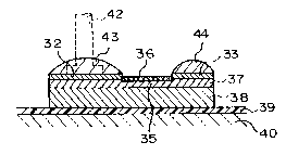
Figure 2 is a plan view of an upper via pad of a
multi-layer ceramic substrate assembly, on which an I/O
; . ,:
~' ' ' ' ' ' "' . ,;:; , . ! , . ., ~
:
200828~
s
pin is to be fixed. This upper via pad includes a via
pad 31, an I/O pin pad 32, a modification pad 33, a
connecting pattern 34 between the via pad 31 and the I/O
pin pad 32, and a connecting pattern 35 between the I/O
pin pad 32 and modification pad 33. The via pad 31 is
electrically connected to a via-conductor in the
multi-ceramic substrate.
Figure 4 is a sectional view of the upper via pad
of Fig. 2 along the line 4A-4A cutting the I/O pin
pad 32, the modification pad 33 and the connecting
pattern 35. The not shown section of the upper pad
cutting from the via pad 31 to the connecting pattern 34
to the I/O pin pad 33 is basically similar to Fig. 5,
although the via pad 31 is connected to a via-conductor
in the substrates as shown in Fig. 1. In Fig. 4, 32
and 33 denote the I/O pin pad 32 and the modification
pad 33 made of a gold, respectively, 36 denotes a solder
dam made of a titanium-nickel intermetallic compound, 37
a top conductor layer made of nickel, 38 a body
conductor layer made of copper, 39 an insulating layer
made of polyimide, and 40 a multi-layer ceramic layer.
In Figs. 2 and 4, the I/O pin and modification
pads 32 and 33 of gold are a good electric conductor and
easily wettable with a solder, and the solder dam 36 of
titanium-nickel is not wettable with a solder. The
conductor layers 37 and 38 of nickel and copper are a
good electric conductor. The nickel conductor layer 37
is inserted as a barrier between the copper conductor
layer 38 and the gold pads 32 and 33, and although still
a good conductor is inferior to copper in the electric
conductivity thereof. The nickel layer 37 is wettable
with a solder, and therefore, requires a good solder
dam. In the prior art, an organic layer of polyimide is
used as the solder dam, but the solder flows along the
interface between the polyimide and the nickel layer
because the solder has a good wettability with the
nickel. To avoid this flow of a solder under the
:-.. :: . : .. . .
..
:: ~ , , - : ::
,: . .: ::: -: . ~ .. .:- : -
: . .
., : .
2008284
-- 6
polyimide, a metal not wettable with a solder was
proposed for use as a connecting pattern, per se, with
an organic solder dam thereon, but this disadvanta-
geously lowered the electric conductivity of the
connecting pattern between the pads. In contrast,
according to the present invention, a metal or a metal
alloy or compound such as a titanium-nickel inter-
metallic compound is used as a solder dam on a
connecting pattern of a good electric conductor metal
such as copper or nickel, and the adhesion of the metal
or metal alloy or compound solder dam to the metal
connecting pattern is strong enough to prevent a flow of
a solder therebetween.
In a preferred embodiment, the above upper via pad
is manufactured as follows. Figure 5 shows a step of
manufacturing the upper via pad of Figs. 2 and 4. A
multi-layer ceramic substrate 40 (e.g., thickness 12 mm)
is prepared in a conventional way. After the polyimide
insulating layer 39 (e.g., thickness 20~m) is formed on
the multi-layer ceramic substrate 40, the copper body
conductor layer 38 (e.g., thickness 4~m) and the top
conductor layer 37 (e.g., thickness 2~m) are formed in
the form of an upper via pad including the three pads
31-33 and the two connecting patterns 34-35, by
sputtering. Then three gold pads 31-33 (e.g.,
thickness 0.5 - 1 ~m) are formed on the nickel top
conductor layer 37 (the plan view shown in Fig. 2) by
plating and selectively etching the gold plating layer
on the connecting patterns 34 and 35.
Then a titanium layer 41 (e.g., thickness 100 nm)
is deposited entirely over the gold pads 31-33, the
nickel connecting patterns 34-35, and the polyimide
layer 39. This is followed by a heat treatment at 500C
for 60-90 minutes, by which the gold pads 31-33 are not
changed and the nickel top conductor layer 37 at the
connecting patterns 33-34 selectively reacts with the
titanium to form a titanium-nickel intermetallic
2~08284
-- 7
compound, Ti2-Ni3. This titanium-nickel intermetallic
compound forms a solder dam 36 covering the nickel top
conductor layer 37 at the connecting patterns 33-34.
Then the ceramic substrate is immersed in a
hydroqen fluoride solvent (about 1% conc.). During this
immersion, the titanium-nickel intermetallic compound on
the connecting patterns 33-34 is not dissolved but
remains, and the titanium layer 41 over the pads 31-33
and the polyimide layer 39 is selectively dissolved.
Thereafter, the upper via pad as shown in Fig. 4 is
obtained. As mentioned before, the gold pads 31-33 are
wettable with a solder but the titanium-nickel
intermetallic compound connecting patterns 33-34 are not
- wettable with a solder, and thus form or function as a
solder dam. Accordingly, a solder dam easily formed on
the connecting patterns.
Moreover, this preferred process of forming the
solder dam does not require a photolithography step,
because the solder dam of the titanium-nickel
intermetallic compound is selectively formed at the
; connecting patterns by the heat treatment, and the
titanium-nickel intermetallic compound acts as a mask in
the following etching step, and therefore, the process
is simple. In contrast, in the prior art, the formation
of a solder dam of a polyimide or the like requires such
a photolithography step.
After formation of the upper via pads, as above,
I/O pins 42 are soldered to the I/O pin pads 32 with a
solder 43 having a relatively high melting point, such
as gold-tin (about 350C). Then, a solder 44 having a
relatively low melting point such as tin (about 250C)
is bonded on the modification pad 33 for later use. The
soldering is carried out by preliminary bonding the
solders 43 and 44 to the pads, setting and fixing the
I/O pins 42 to the I/O pin pads, and carrying out a
` reflow heat treatment in an oven (at about 350C),
whereby a multi-layer ceramic substrate assembly or
:`
... .: , . .
2008284
-- 8 --
connector is produced.
When the original circuit of the assembly is to be
changed, discrete wires are used to connect between
desired I/O pins and/or via conductors, and the
disconnection of the I/O pins from via conductors is
made by cutting the connecting pattern between the I/O
pin pad and the via pad, usually by a laser. The wires
are bonded to desired modification pads with the solder.
This soldering can be conducted at a relatively low
temperature (about 250C) at which the solder fixing the
I/O pins to the I/O pin pads 32 is not damaged, because
the solder fixing the I/O pins has a relatively high
melting point (about 350C). Note, during this heat
treatment for soldering the wire to the modification
pad, the solder cannot flow to the I/O pin pad 32
because of the presence of the solder dam 36.
It should be noted that the present invention is
not limited to the above preferred process of forming
the solder dam, and is applicable to any solder dam made
of a metal or a metal alloy or compound not wettable
with a solder in combination with another metal
connecting pattern having a good electric conductivity.
EXAMPLES
Solder dams were formed from various materials, and
the flow of the solder through the solder dam was
examined. Figures 6-ll show the results after a heat
treatment at 350C for 3 minutes. The photographs were
taken at a magnification of 50. In Figs. 6-8, the upper
pad is an I/O pin pad, the lower left pad is a via pad,
the lower right pad is a modification pad, and the
connecting patterns can be seen between the pads.
Figures 9-ll are symmetrical to Figs. 6-8 at the left
and right sides thereof.
Figure 6 shows the results obtained with a solder
dam formed of the titanium-nickel intermetallic compound
made as described above; the results are good in that no
solder flows onto or through the solder dam.
- - 2008284
g
Figure 7 shows the results obtained with a solder
dam of sputtered chromium. The results are good in that
no solder flows onto or through the solder dam.
Pigure 8 shows the results obtained with a solder
dam of sputtered chromium with a coat of polyimide
' thereon. The results are good in that no solder flows
onto or through the solder dams.
Figure 9 shows the results obtained with a solder
dam of plated gold. The results are not good in that
solder flows onto and through the connecting patterns:
The black at the connecting patterns indicates the
flowed solder; the partially seen white is due to light
' reflection when taking the photo.
Figure 10 shows the results obtained with a solder
dam of polyimide over plated gold connecting patterns.
The results are not good in that solder flows partially
under the left hand solder dam and onto the right hand
solder dam; the right hand connecting pattern having a
dark color in comparison with the whiteness of
Figs. 6-8, indicating a flow of solder in the lower
layer.
Figure 11 shows the results obtained with a solder
dam of sputtered nickel. The results are not good in
that solder flows into and through the right hand solder
dam, and a similar solder flow will occur at the left
hand solder d~m.
.
,