Note : Les descriptions sont présentées dans la langue officielle dans laquelle elles ont été soumises.
- 1 -
A method of arranging signal points in a
quadrature amplitude modulation/demodulation system
Background of the Invention
Field of the Invention
The present invention relates to a method of
arranging signal points on a complex plane in a
quadrature amplitude modulation/demodulation system
and a quadrature amplitude modulator/demodulator
device using this method.
10 Description of the Related Art
Recently, various types of high-speed modems
which modulate and transmit digital signals at high
speed have been manufactured as significant
improvements have been made in the processing power of
15 digital-signal processing LSIs. In order to implement
high-quality data transmission using high-speed
modems, it is essentlal to introduce a
modulation/demodulation system which is capable of
maximizing the signal-to noise ~S/N) ratio while
20 minimizing transmission error rate.
To provide efficient communication, tha
quadrature amplltude modulation/demodulation system is
adapted to tr~ansmit as much digital data as possible
within a limited transmission bandwidth. In this
25 ~system, a~ correspondence is established between M
,. .. ..
' ' ; : .' ' ' .. ~ ' ' ' ' ~': ' . ~' - ' ; ',, ,: ". ' . ' . '' : ' ,, ,'
: . . ~ - .: : , . .
. -
. : : .,: . . , . .~: - - - :. :
2~ V9
-- 2
kinds of data patterns represented by log2M bits and M
signal points on a complex plane. Two carrier
components cos ~t and sin~ t ( ~ is angular frequency
of carriers and t is time), which are 90 apart in
phase, are amplitude modulated with a real value and
an imaginary value, respectively, indicating
coordinate data of each signal point on the complex
plane. The resulting amplitude modulated carriers are
added to produce a combined modulated signal for
transmission. On the other hand, the demodulation
side multiplies the modulated signal by sin ~t and
cos ~ t to extract the real value and the imaginary
values. A corresponding one of the M signal points is
identified by these values so that M kinds of data
patterns are demodulated.
In this case, parameters such as the S/N ratio
and transmission error rate of a data transmission
device, depend upon the way signal points are
arranged on the complex plane. In general, to
implement a signal point arrangement for achieving
good transmission performance, two conditions should
be satisfied.
First, the transmission error rate depends on the
distance between signal points on the complex plane.
That is, where a signal point is identified by a
. '. ' '
- '
~ - :
- 3 - 2~ 9
modulated signal in the demodulation system, if the
distance between signal points is too small on the
complex plane, a signal point adjacent to the true
signal point may be extracted erroneously. To secure
a low transmission error rate, therefore, the distance
between each pair of signal points on the complex
plane must be accurately determined. In particular,
in order to secure a low, constant transmission error
rate among signal points, the distance between
adjoining signal points should be constant.
1 0
Second, in general, when a transmitter is
supplied with high-power modulated signals, its output
is liable to saturate, thus increasing transmission
error. The power of modulated signals must therefore
be made as low as possible so as to decrease
transmission power. The peak power of modulated
signals in particular must be ~ade as low as possible.
It is known that the power of a modulated signal based
; on a signal point on the complex plane is proportional
to the square of the distance between the signal point
and the origin of the complex plane. It is also known
tha~t~the farther a signal point is from the origin,
the higher is the power of a modulated signal
corresponding to that signal point. In order to lower
~. ~
the power of modulated signals, therefore, it is
: `
~ ~ .
,`' '. ' ., ~.. ' ` ' - ~ '
,, ~ . . -
~ ' , , .
2i~ 9
required to arrange each signal point as close to the
origin as possible.
A conventional method of arranging signal points
in a quadrature amplitude modulator/demodulator device
5 is described below, taking the above two conditions
into consideration.
A first prior art signal point arranging method,
is shown in Fig. 1A. Here, signal points are
arranged in an 8 x 8 grid-like pattern on a phase
10 plane with an outward form of a square. A second
prior art, signal point arranging method is shown in
Fig. 1B. Here, four corners of a square are cut away.
According to both of these prior art methods, the
distance between signal points can be made constant,
15 thus meeting the first condition. There is also an
integral-multiple relationship in each of the real and
imaginary values in coordinate data between signal
points, thus permitting such modulator/demodulator
devices to be simply constructed. In both the first
20 and second prior arts, however, no measures are taken
to bring the~signal points as close to the origin of
: : : : . ,
; the complex plane as possible, thus ~ailing to meet
the above second condition. Therefore, a problem
ari~ses in that the pe~ak power of modulated signals
~; 25 cannot be made sufficiently low, thus making the
: ::
.
.
: .
: :
_ 5 _ 2
transmission error rate high.
Next, as a third prior art, there is known a
signal point arranging method, which is disclosed in
published examined Japanese Patent Application No. 63-
5 24342. Here, signal points located at cornersdistant from the coordinate axes of the complex plane
are relocated close to the coordinate axes, thereby
decreasing signal transmission power. With the third
prior art, however, there is no diagrammatic
10 regularity for relocating signal points on the complex
plane. When the number of signal points is increased,
they have to be relocated by trial and error, thus
making the process troublesome.
As a fourth prior art, there is known a signal
15 point arranging method, which is disclosed in
published unexamined Japanese Patent Application No.
60-150359. Here, signal points are arranged on
concentric circles disposed at equal intervals and in
~ this case the signal polnts are determined so that the
20 distance between them may have almost a predetermined
value. In the case of this prior art, each signal
point is arranged so that it may be brought as close
as possible to the origin of the complex plane, thus
complying with the above second condition. With the
25 fourth prior art, however, signal points have to be
.
. .
.
.. : : ' ,. :.
. . . . :
.: . . : .
.
. . . , . .. .. . ; :
6 2~
positioned on each of the concentric circles by trial
and error so that the distance between the signal
points may be equa] to or more than the predetermined
value, thus making the logic for the signal point
5 arrangement very difficult. In particular, it is
necessary to measure and evaluate the distance between
signal points each time a signal point is arranged.
As can be seen, a problem with the fourth prior art is
that the arrangement of signal points cannot be
10 determined readily.
Summary of the Invention
Considering the disadvantages of the arts
described above, it is an object of the present
invention to minimize the peak power of modulated
15 signals, reduce transmission error rate and optimize
S/N characteristics with the distance between signal
points nearest to each other being held constant on a
phase plane by a simplç process without losing
diagrammatic regularity.
20~ That~is, the present invention is premised on a
signal point arranging method for use with a
quadrature amplitude modulator/demodulator device in
which a;desired number of signal points is~arranged on
a rectangular plane. The method comprises a grid
~ 25 setting step, a concentric circle setting step and a
:
`'' ' . ~ ' '` ''
` ` , ~. ~ `
-,,: ' . : ' - : . . : `
_ 7 _ 2
signal point arranging step. First, in the grid
setting step, a plurality of grid points spaced a unit
distance apart are set symmetrically with respect to
the rectangular coordinate axes of the rectangular
5 plane. The rectangular plane may be, for example, a
phase plane, and the grid may be, for example a
square grid or a equilateral triangular grid.
Next, in the concentric circle setting step, a
plurality of concentric circles, each having a radius
10 equal to a distance between the coordinate origin and
a grid point, are set with center at the coordinate
origin of the rectangular plane.
Then, in the signal arranging step, a desired
number of signal points is arranged on intersection
15 points of the concentric circles and on grid points in
increasing order of circles in radius beginning with
the smallest. In this case, the signal points to be
arranged on the outermost circle may be arranged at
locations which are symmetrical with respect to the
20 coordinate orlgin.
.
In such a signal arranging method as described
above, by sequentlally arranging signal points on the
concentric circles with increasing radii beginning
: : :
with the smaIlest, each of the signal points can be
25 arranged as close to the coordinate origin as
:
:
- : . , ., " :', ' ...... ; '' ' . .'. . ': :":~ '. ' ,
:- . . . . . . . . . .
- 8 - 2~ 9
possible, thus enabling the peak power of modulated
signals to be minimized. In addition, by arranging
the signal points at intersections of the grid spaced
a unit distance apart, the distance between signal
points can be held constant. Thus, the S/N
characteristic does not vary with the signal points
and a low constant transmission error rate can be
secured. As a result, a signal point arrangement is
obtained which enables data transmission at minimum
10 required power, reduces transmission error rate and
optimizes the S/N characteristic.
Brief Description of the Drawings
The foregoing aspects and the other features of
the invention may be understood by those skilled in
15 the art with reference to the following description of
a preferred embodiment of the invention, taken
together with the accompanying drawings in which:
Figure 1A is a diagram for explaining a first
conventional signal arranging method,
~; 20 Figure 1B is a diagram for explaining a second
conventional signal arranging method,
Figures 2A, 2B and 2C are diagrams for explaining
,
the principle of the invention;
Figure 3 is a schematic diagram of a modem
25 according to an embodiment of ~he invention; and
: '
. . : .. . , , : , . . . . :: .
:.~ : .. .. - . . - . : . , -
.:
.. .. . . . .
:.' : : ,
2~ l09
g
Figure 4 is a diagram for explaining a signal
arranging method of the invention.
Description of the Preferred Embodiment
The principle of a signal point arranging method
according to the present invention will be described
first with reference to Figures 2A, 2B and 2C.
The subject of this invention is a signal point
arranging method for arranging a desired number of
signal points on a phase plane for use with a
10 quadrature modulator/demodulator device.
First, as shown in Fig. 2A, a grid 1 is set,
which is symmetrical with respect to the rectangular
coordinate axes of a phase plane, i.e., a complex
plane, and which has intersection points disposed at
15 regular intervals of a unit distance.
Next, as shown in Fig. 2B, concentric circles 2
are set with their centers at the origin O on the
phase plane, each having a radius equal to the
distance between origin O and corresponding
20 intersection points of grid 1.
Then, a required number of signal points 3 are
placed at the intersection points of grid 1 and each
of circles 2 beginning with the smallest and
.
cont~inuing with circles of increasing radius.
~ According to this signal point arranging method,
::
.
~ .
,
.. . . . . . .
. .
., . , ., . :. , , . : . : -
. . - . : :: . . : . .
2~ 9
- 10 -
by placing signal points 3 on concentric circles 2
with their center at origin O, each of the signal
points 3 can be placed as close to the origin O as
possible, thereby minimizing the peak power of
5 modulated signals.
Also, by placing signal points 3 at intersections
of grid 1 which are spaced a unit distance apart, the
distance between signal points can be held constant,
so that the S/N ratio remains unchanged at each of
10 signal points 3, thereby securing a low, constant
transmission error rate.
As a result, a signal point arrangement is
obtained, which enables data transmission with minimum
required power transmission error rate to be reduced
15 and S/N ratio to be maximized.
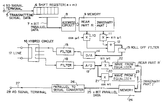
Figure 3 illustrates an embodiment in which the
above-mentioned signal-point arranging method is
applied to a modem for a digital data circuit. On the
transmission side of the modem, serial data to be
20 transmitted is split into parts, each of n bits. The
n-bit data is allotted to one of 2n signal points on a
phase plane as pattern data and is modulated for
: : :
transmission. On the demodulation side of the modem,
a decision is made as to which of 2n signal points
25 corre~ponds to the modulated data from the
.
, ; ,- ~ : .
-, . ~ . . , . -
... .. .: .. . .. . . :
.
. . , .. :- . :
,.
2~ o~
transmission side and then the received serial data of
n bits for the corresponding signal point is
demodulated.
First, the arrangement of the transmission side
5 will be described.
Serial data 5 to be transmitted is supplied to an
SD signal terminal 4 from a data sending terminal (not
shown) and then serially entered into a shift
register 6 having n~m stages from which n-bit parallel
10 data is outputted.
Parallel data 7 is inputted to an address circuit
8, which in turn supplies address data corresponding
to parallel data 7 to a memory 9. Memory 9 stores 2n
sets of a real part R and an imaginary part I which
15 respectively correspond to real coordinate data and
imaginary coordinate data of each of 2n signal points
on the phase plane. Each value of the real part R and
the imaginary part I is determined on the basis of the
signal point arranging method, to be described later.
Real part I and imaginary part I, read from a
location of memory 9 specified by address circuit 8,
are inputted to multipliers 10 and 11, respectively,
~:~ so that they are multiplied by cos ~ t and sin ~ t.
Here ~ is angular frequency of a carrier and t is a
25 time variable which increases with time. In this
.
., ,
. .' ` ' ' : .- -
: . '
, ~ ' ' ,
.
.
,:, . :
2~ 09
- 12 -
manner two carrier components cos ~t and sin(~ t are
amplitude modulated by the real part I and the
imaginary part I, respectively.
output signals of multipliers 10 and 11 are added
5 together in an adder 12 and then applied to a roll-off
filter to extract a baseband component. The baseband
component is converted to an analog modulated signal
by means of a digital to analog (D/A) converter 14 and
a filter 15. The analog modulated signal is then
10 applied to a hybrid transformer circuit 16 and sent
out to a circuit 17 as a transmission signal.
The arrangement of the receiving side will now be
described.
A modulated signal transmitted over circuit 17 is
15 applied to a filter 18 via hybrid circuit 16 and then
converted to a digital signal by an analog to digital
(D/A) converter 19.
The received signal is multiplied by sin~ t and
cos ~t in multipliers 20 and 21 for synchronous
20 detection of the real and imaginary parts. ~he real
and~ imaginary parts are applied to waveform equalizers
22 and 23, respectively, thus equalizing signal
degradation suffered ln the circuit. The real part R'
and the imaginary part I' outputted from waveform
.
25 egualizers 22 and 23 are supplied to a me~ory 24.
` : :
.
- 13 - 2~
Memory 24 stores 2n sets of n-bit parallel data
corresponding to 2n signal points on the phase plane.
The corresponding relationship between the signal
points and the parallel data is the same as that on
5 the transmitting side. Memory 24 is arranged to
output n-bit parallel data corresponding to a signal
point near to a point on the phase plane which is
defined by real part R' and imaginary part I' as data
25.
The n-bit parallel data 25 is entered into a
parallel to serial converter 26 in no bit units.
Parallel data 25, which is entered in n-bit unit, is
converted to serial data by parallel to serial
converter 26 and then outputted to a data receiving
15 terminal (not shown) via an RD signal terminal 28 as
serial received data 27.
An embodiment of the method of arranging 2n
signal points, each defined by a set comprising a real
part R and an imaginary part I stored in memory 9 in
20 the modem arranged as above on the phase plane, is
described below. This embodiment is based on the
~signal arranging method described before with
reference to Figs. 2A, 2B and 2C. A description is
made here of a signal arranging method where n = 6,
25 i.e., 2n = 64, in Figure 3, and grid 1 (refer to Fig.
:. ~: , ,: ~
~Q~O~
- 14 -
2A) is a square grid.
In this embodiment of the signal point arranging
method, signal points are arranged as show in Fig. 4
in accordance with the following procedure.
(1) A square grid 29 whose intersection points
are spaced unit distance apart is provided so that the
grid may be symmetrical with respect to the orthogonal
coordinate axes A (real axis) and B (imaginary axis)
of a phase plane~
(2) Concentric circles 30 are set each having a
radius equal to the distance between origin O and an
intersection of square grid 29.
(3) 64 signal points 31 are arranged on
intersection points of square grid 29 and each of
15 concentric circles 30, beginning with the smallest
and continuing with circles of increasing radius.
(4) A set of each of signal point 31 comprising a
real part (value on coordinate axis A) and an
imaginary part (value on coordinate axis B) is stored
20 in memory 9 of Fig. 3.
In the signal point arrangement of Fig. 4, the
outermost circle 30' has eight locations on which
signal points 31 are to be arranged. In fact,
however, signal points 31 are arranged at four
25 locations only. In terms of phase balance these four
'' '
2~ .09
- 15 -
locations should be arranged point-symmetrically with
respect to the coordinate origin O. That is, assuming
that sets of real part R and imaginary part I for
signal points 31 are selected randomly in memory 9 of
Fig. 3 at the time of modulation, if signal points are
provided at locations which are point symmetrical with
respect to the coordinate origin O, distributions of
frequency at which the four signal points are selected
will become symmetrical with respect to each of real
axis A and imaginary axis B. This will allow analog
signal processing, such as filtering, to be performed
easily.
In memory 9 of Figure 3 are stored sets
comprising a real part R and an imaginary part I, each
corresponding to a separate one of the signal points
arranged by the above-described method. Each of the
sets is selected, as described above, by an address
generated by address circuit 8 on the basis of n-bit
parallel data 7. In this case, a correspondence
~ - 20 between n-bit parallel data 7 having 2n patterns and
2n signal points may be established such that patterns
having a high frequency of appearance are sequentially
allotted to signal points 31 on concentric circles 30
of lncreasing radius~ Since, as described above, the
25` power of a modulated signal for each signal point is
' ,; ''~' ~ :
.
, :
~ 9
- 16 -
proportional to the square of the distance between the
coordinate origin O and the signal point, the average
transmission power of modulated signals can be lowered
and transmission error rate can be reduced by the
5 established correspondence described above.
In the present embodiment, as described above, a
plurality of concentric circles 30 is drawn on a phase
plane as shown in Fig. 4 and signal points 31 are
sequentially arranged on concentric circles 30 of
10 increasing radius, thereby enabling transmission at
minimum power. As a result, the output voltage on the
transmission side of the modem can be lowered, and
each input signal accurately on the receiving side of
the modem can be received and identified even if the
15 received signal has a small dynamic range. This will
allow the modem to be formed of inexpensive devices
adapted to handle lower power, thereby reducing
overall cost.
By setting square grid 29, by providing
20 concentric circles 30 each having a radius equal to a
distance between the coordinate origin O and an
inter~section of square grid ~9 and by arranging signal
points 31 on points of intersection between concentric
circles 30 and square grid 29, it becomes possible to
: -
25 hold the distance between signal points constant,
: :
'
.
- - ..- :. . , . . . - : ~
- ,
- . .. . , ~. . ~:
. - . -: . . .. : . ,, ~ , . . .
2~ 9
- 17 -
thereby permitting the S/N ratio to be made constant
for each of the signal points.
In particular, by adopting square grid 29, a
modulator/demodulator device can be constructed using
5 a simple address circuit and memories, as in the above
first and second prior arts based on the square
arrangement.
Square grid 29 is used in the above embodiment.
Alternatively, an equilateral triangular grid may be
10 used in order to make the distance between signal
points constant. Where an equilateral triangular grid
is used, the condition for the closest signal points
can be satisfied, thereby optimizing the S/N
characteristic. In this case, as is the case with
15 Fig. 4, concentric circles each having a radius equal
to a distance between the coordinate origin O and an
intersection of the equilateral triangular grid are
set and a required number of signal points are
sequentially arranged on intersection points between
20 the equilateral triangular grid and concentric circles
:
of increasing radius.
To make the distance between signal points
constant, other suitable grid structures than the
above-mentioned square and equiIateral triangular
25 grids may be used.
- . . . . . - . .
- : : , : ,. .
.
,: ......
,
..
~: ~ : . -, . :
. - , ' ''
- 18 -
Where the signal point arranging method according
to the present invention is used, the S/N
characteristic will be improved by about 0.1 dB when
the number of signal points is 16 and by about 0.2 dB
5 when the number of signal points is 256.
1 0
:
':
: ..... ~ -. , . :
.
., . - : , .