Note : Les descriptions sont présentées dans la langue officielle dans laquelle elles ont été soumises.
-1 - RCA 85,453
a~.c~B I~LT~R EQU_~ CY F~E~S~I~E ~.~'~~ i
This invention relates to television receivers of the
type employing comb filters for providing luminance and
chrominance signal separation and particularly to receivers in
which the comb filter exhibits a non-uniform amplitude
response with frequency and in which a compensation circuit is
provided for reducing the response variations.
The advantages of using a comb filter for providing
luminance and chrominance signal separation in a television
receiver are quite well known. A conventional comb Titter '
includes a delay device for imparting a one horizontal line (1-H)
delay to the video input signal, an adder for adding the delayed
and non-delayed input signals to provide a luminance output
signal and a subtractor for subtracting the delayed and non-
delayed signals to provide a chrominance output signal.
The delay element used in a comb filter has a very
significant effect on the comb filter frequency response
characteristic. The ideal delay element would have a constant
delay independent of frequency thereby providing a linear phase
response and thus a uniform amplitude response throughout the
video frequency band to be filtered. The delay element presently
closest to this ideal is the digital delay line employing binary
storage elements. Unfortunately, digital delay lines are costly
and relatively complex because video signals are conventionally
received in analog form and so conversion to digits! form is
necessary to use digital delay lines of the binary storage type.
Analog delay elements, such as glass delay lines, are
conventionally used in comb filters as a means of reducing the
cost and complexity of the filter. Comb filters employing glass
delay elements (or other analog delay elements) are however
subject to delay variations with frequency (i.e., non-linear phase
response) and thus
the overall amplitude response of such comb filters tends to
vary with frequency.
Manufacturers of comb filters of the glass delay line
type have recognized this problem and have taken steps to
correct for undesired amplitude variations which, 'to a certain
- 2 - RCA 85,453
extent, minimizes the problem. As an example, amplitude ~
response 2 of FIGURE 2 (PRIOR ART) herein illustrates the
uncorrected response of a commercially available comb filter
employing a glass delay line. As shown, the uncorrected
response exhibits a rising response from about 2.5 MHz to 4.5
MHz with a peak of about +6dB. The manufacture of this filter
has included a correction circuit having the characteristic
shown by response ~. The resultant corrected response is
illustrated by curve 4. As seen the amplitude corrected comb
filtered signal (4) exhibits a dip of about 2dB at a frequency of
about 2.5 MHz, it returns to zero dB at about 3 MHz and a
decreases thereafter. As shown, the rather large 6dB variation
of the uncorrected comb filter has been reduced to only 2dB by
internal correction circuits provided by the manufacturer (TDK
Incorporated, mode! HCF0020C).
The comb filter correction (to 2dB) provided by the
filter manufacturer is quite good considering the rather large
(+6dB) variations typical of uncompensated comb filters with
glass delay lines. It has been recognized by the present
inventor, however, that it would be desirable to provide a
further correction of the comb filter response to reduce the
luminance signal variations to a few tenths of a decibel in the
luminance frequency range. To this end the present inventor has
previously designed a receiver in which an auxiliary luminance
amplitude correction circuit was included which achieved this
goal. This receiver has been manufactured and sold under the
brand name "RCA" in receivers employing chassis identification
numbers CTC 141149 and is shown herein as FIGURE 1 (PRIOR
ART). An understanding of this prior art receiver (10) is helpful
to appreciating the subtle nature
of the present invention and so this receiver will now be
described in detail.
Receiver 10 includes an RF processor i 2 having an
antenna or cable input terminal 14 for receiving an RF video
input signal S1. Processor 12 includes conventional elements
such as a tuner for selecting channels, an IF amplifier and sound
trap and a video detector for providing a demodulated (baseband)
composite video output signal S2 at its output. A video switch
3 - R.CA 85,453
14 is provided for selecting signal S2 or an auxiliary composite
video baseband signal S3 applied to an auxiliary input terminal
16. The selected signal S4 provided by video switch 14 is
applied to a comb filter 18 of the type employing an analog type
delay element (e.g., a glass delay line). The ~fiiter 18 exhibits
uncompensated amplitude variations as a function of frequency
and has a luminance signal output 20 for providing a luminance
output signal Y1 and a chrominance signal outlput 22 for
providing a chrominance output signal C1.
The chrominance signal C1 is applied to a first input
24 of a luminance-chrominance (Y-C) processor 26. The
luminance signal Y1 is applied to a second (luminance) input 28
of processor 26 by means of a cascade connection comprising, in
the exact order named of: a contrast control 30, a
luminance/chrominance delay correction circuit 32 having
source (R1 ) and termination (R2) resistors and a comb filter
correction circuit 34 (outlined in phantom).
The function of contrast control 30 is to control the
peak-to-peak amplitude of the comb filtered luminance signal.
In the prior art receiver this control is provided by a 300 Ohm
potentiameter coupled in series with a 430 Ohm resistor, the
latter serving as a minimum limit to the potentiometer output.
The function of lama delay 32 is to delay the comb filtered
luminance signal by about 300 nano-seconds. This compensates
for difference in luminance and chrominance signal delay in the
receiver due to their different bandwidths and thus provides
proper registration
of the luminance and chrominance signals for display on display
36. The function of the comb filter correction circuit 34 is to
correct uncompensated errors in the amplitude response of comb
filter 18. This correction is shown in FiOURE 2 by curve 5 which
has a +2dR peak at a frequency of about 2.5 MHz. As a result the
uncorrected comb filter output (response 4) is flattened to the
response 6 which is essentially constant up to a frequency of
about 4.2 MHz, the full extent of the lama band in the iVTSC
standard. Processor 26 includes conventional circuits for
providing functions such as chrome demodulation, hue and
- 4 - RCA 85,453
saturation control and matrixing for providing a suitable output ,
regional (e.g., RGB) for display by display unit 36.
The correction circuit 34 (outlined in phantom)
comprises an input ~.0 connected to the output 38 of lama delay
unit 32 (e.g., 300 nanoseconds) and an output ~2 connected to
input 28 of processor 26. Internally unit 34 includes a parallel
resonant circuit comprising an inductor L1 and a capaitor G1
connected in common to terminals 40 and 42 at one end thereof
and coupled to ground at the other end thereof by means of a
resistor R3. Representative values for L1, G1 and R3 are 100
micro-Henrys, 39 pico-Farads and 8200 Ohms, respectively.
This circuit provides the lama signal boost of about 2dB shown
in FIGURE 2 as response 5 which flattens the overall response 6
to within less than 1dB over the full lama band as shown.
It is herein recognized that the substantial
improvements in comb filter performance provided by the
present inventor in the design of the prior art receiver of FIGURE
1 can be improved to an even higher standard of performance.
Specifically, it has been discovered that slight image blurring
may occur in the PRIOR ART example of FIGURE 1.
The present invention resides in: (1) discovery of the
existence of the problem ~f image distortion in the
prior art receiver, (2) discovery of the cause of the problem and
(3) discovery of solutions which are both technically effective
and cost effective.
The cause of this problem has been found, in
accordance with the present invention, to be related to the
specific point in the prior art receiver 10 where the luminance
signal amplitude correction circuit 34 is connected. In
particular, the connection of circuit 34 has been discovered to
cause reflections in delay line 32. The visual effect of these
reflections or "ringing" is to create double images or ghosts of
very short displacement relative to the main image and thus may
be manifested visually as image blur.
In accordance with another aspect of the invention,
the technical reason that delay line 32 exhibits ringing is two
fold. Specifically, the delay correction circuit 34 exhibits a
frequency dependent impedance variation because the impedance
- 5 - RCA 85,453
~~.~~~~
of elements L1 and C1 changes with frequency. The luminance
delay circuit 32, however, is a conventional analog delay line
and so is sensitive to variations in impedance of its source and
load elements. lNith circuit 34 directly connected to the load
resistor R2 of delay line 32 the effective load impedance thus
varies with frequency thereby causing frequency dependent load
variations for delay line 32.
In accordance with an aspect of the invention the
receiver is provided with circuit means for preventing
impedance variations of the comb filter correction circuit from
causing reflections in the luma delay line. A number of
examples using isolation amplifiers are given herein for
providing substantially constant source and termination
impedances for the luminance delay line to prevent the
reflections.
In a preferred application of the principles of the
invention, the reflections are prevented utilizing existing
receiver components thus eliminating the need for an isolation
amplifier.
The cost effectiveness of the preferred embodiment
is readily apparent, Additionally, there is a technical advantage
obtained in that by eliminating the need for an active circuit
element (isolation amplifier) the reliability of the receiver is
enhanced.
In accordance with the preferred embodiment of the
present invention, the comb filtered luminance signal amplitude
correction is applied between the output of the video source
(switch 14} and the input of the receiver comb filter (18).
The invention is illustrated in the accompanying
drawing wherein like elements are denoted by like reference
designators and in which:
FIGURE 1 is a diagram in block and schematic form of
a PRIOR ART receiver having correction for the response of a
comb filter employing a glass delay line element;
FIGURE 2 is a response diagram of a PRBOR ART comb
filter employing a glass delay element and illustrates response
corrections used by a filter manufacturer and a receiver
manufacturer to correct for amplitude errors of the comb filter;
- 6 - RCA 85,453
FIGURES 3, 4 and 5 are diagrams in block and
schematic form of a television receiver embodying the~'~~-~~~
invention; and
FIGURE 6 is a diagram in block and schematic form of
a preferred embodiment of a television receiver embodying the
invention.
Prior art FIGURES 1 and 2 have been previously
discussed in detail.
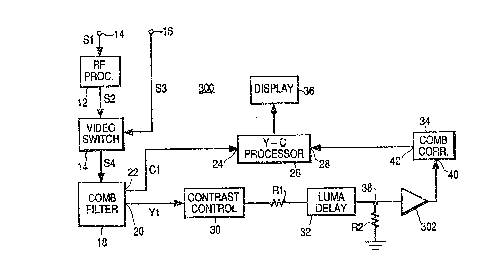
The receiver 300 of FIGURE 3, embodying the
invention is similar to receiver 10 of FIGURE 1 but differs in
that a buffer or isolation amplifier 302 is interposed in the
circuit path (30,32,34} between the output 20 of comb filter 18
and the luminance input 28 of Y-C processor
26. Specifically, in this embodiment the amplifier 302 is
connected between the output 38 of lama delay filter 32 and the
input 40 of comb filter correction circuit 34. accordingly, the
impedance variations of comb filter correction circuit 34 are
effectively isolated from the output of lama delay circuit 32
and thus the effective load impedance for circuit 32 is
stabilized. This prevents reflections in line 32 and solves the
newly discovered problem with the prior art receiver.
The receiver 400 of FIGURE 4, embodying the
invention, is similar to receiver 10 of FIGURE 1 but differs in
three respects. Specifically, (1} the output 38 of lama delay
line 32 is connected directly to the input 28 of processor 26
thus stabilizing the termination impedance of delay line 32. To
provide comb filter frequency correction, a correction circuit
402 is connected at the output of contrast control 30. To
prevent impedance variations of circuit 402 from varying the
effective source impedance (R2} of lama delay line 32, an
isolation or buffer amplifier 404 is connected between the
output of comb correction circuit 402 and the source resistor R1
for lama delay circuit 32. The connection of lead (termination)
resistor R2 directly to input 28 of processor 26 eliminates load
impedance variations. The use of isolation amplifier 404
prevents source impedance variations. Thus no reflections are
produced in delay line 32 by impedance variations of correction
circuit 402.
-'7 - tZCA 85,453
The receiver 500 of FIGURE 5 is similar to that of
FIGURE 4 except that comb filter correction and isolation is
provided before contrast control 30. Specifically, the output 3a
of delay line 32 is connected directly to the input 23 of y-C
processing unit 26 and a comb filter amplitude correction
circuit 502 is connected to the comb filter output 20 and
coupled via an isolation amplifier 504 to the input of the
contrast control 30.
The output connection of delay line 32 prevents load
impedance variations. Comb filter correction is provided by
relocating the correction circuit to the comb
output 20. Source impedance variations are prevented by
isolation amplifier 504. Accordingly, the load and source
impedances of line 32 are constant and reflections are thereby
suppressed.
The receiver 600 of FIGURE 6 is a presently
preferred embodiment of the invention. This embodiment of 'the
invention utilizes existing receiver circuits to solve the same
newly discovered problem as the embodiments of FIGURES 3, 4
and 5 but this is achieved without requiring the use of an
isolation amplifier. As previously explained, this provides two
additional advantages of the invention including:
(1) a superior technical effect and
(2) an economic benefit.
The economic benefit obtained by solving a problem
using existing circuits without need for an isolation amplifier
will be readily apparent to anyone concerned with the
manufacture of television receivers. The superior technical
effect obtained is an improvement in receiver reliability by
elimination of the need for the isolation amplifier. The task of
the quality control engineer is thus simplified because 'there is
one less active amplifying component to fail when using the
preferred embodiment of the invention.
In detail, in the embodiment of FIGURE 6, the comb
filter correction circuit is relocated. Specifically, the
following changes have bean made in the receiver 10 of FIGURE 1
to implement receiver 600 of FIGURE 6:
g - RCA 85,453
~~.(~~6~
(9 ) the output 38 of lama delay fine 32
has been connected directly (by means of
connection 802) to the input of Y-C
processor 26; and
(2) the comb filter correction circuit 34
has been relocated between the output 20
of video switch 14 and the input of comb
filter ~ 8.
More specifically, in this embodiment of the
invention the output 20 of video switch i4 is cormected to input
40 of comb filter correction circuit 34 the output 42 of which is
connected to the input of comb filter 18. Ry this connection the
source and termination impedances of luminance signal delay
line 32 are not influenced by impedance variations with
frequency of the comb filter correction circuit 34 and thus the
image blur problem is solved with the technical and economic
advantages noted above. 1n this new location of circuit 34
exemplary element values of L1,C1 and R3 are 47 micro-Henrys,
82 pico-Forads and 1 X00 Ohms, respectively. Also a series
input resistor R5 (e.g., 390 Ohms) has been added and the L-C
elements L~,C~ are coupled to a supply terminal ~3 rather than
to ground. 'fhe DC path thus provided (L.1,R3,R~) advantageously
provides DC bias to the input ofi comb filter 18 which employs an
input amplifier biased by the video signal DC input component.
Advantageously, the DC bias applied by correction circuit 3~
eliminates the need for a separate bias network and blocking
capacitor for comb filter 18.