Note : Les descriptions sont présentées dans la langue officielle dans laquelle elles ont été soumises.
- 1 - 201.0673
RD-17,680
CURRFNT CHOPPING STRATEGY FOR SWITCHED
RELUCTANCE MACHINES
Field of the Invention
The present invention relates generally to
switching control and current regulation in bridge inverters.
More particularly, this invention relates to a method and
apparatus for controlling the switching devices and
regulating current in a switched reluctance machine bridge
inverter.
Background of the Invention
A switched reluctance machine (SRM) is a brushless,
synchronous machine having salient rotor and stator poles.
There is a concentrated winding on each of the stator poles,
but no windings or permanent magnets on the rotor. Each pair
of diametrically opposite stator pole windings is connected
in series or in parallel to form an independent machine phase
winding of the multiphase SRM. Ideally, the flux entering
the rotor from one stator pole balances the flux leaving the
rotor from the diametrically opposite stator pole, so that
there is no mutual magnetic coupling among the phases.
Torque is produced by switching current in each
phase winding in a predetermined sequence that is
synchronized with angular position of the rotor. In this
way, a magnetic force of attraction results between the rotor
poles and stator poles that are approaching each other. The
current is switched off in each phase before the rotor poles
nearest the stator poles of that phase rotate past the
aligned position; otherwise, the magnetic force of attraction
would produce a negative, or braking, torque. In a SRM,
torque direction is independent of current direction.
Therefore, in contrast to most other brushless machines which
require bidirectional phase currents, a SRM power inverter
- 2 - 2010673
RD-17,680
can be configured to enable current flow in only one
direction through a phase winding. Such an inverter
generally employs one or more switching devices, such as
transistors or thyristors, in series with each machine phase
winding. Advantageously, the switching devices prevent
"shoot-through" current paths. Exemplary SRM converters are
illustrated in commonly assigned U.S. Patent No. 4,684,867,
issued to T.J.E. Miller on August 4, 1987, which is hereby
incorporated by reference.
At relatively low and medium speeds, current
magnitude regulation in SRMs is typically achieved by
hysteresis band current chopping. In a SRM drive employing
two switching devices per phase, such a current chopping
scheme involves generating a commanded reference current
î5 waveform which has predetermined upper and lower hysteresis
band limits to which the phase currents are continuously
compared. At the start of a conduction interval for one
phase (i.e., when a phase is excited for torque production),
the switching devices in series with the corresponding phase
winding are simultaneously switched on. With both switches
thus conductive, current from the DC source builds in the
phase winding until the upper limit of the hysteresis band is
reached. At that point, both switching devices are turned
off. Flyback or return diodes coupled to the phase winding
provide a current path back to the DC source. When the phase
current decreases to the lower limit of the hysteresis band,
the switching devices are switched on again, and the process
repeats. This process is commonly referred to as pulse width
modulation (PWM) or current chopping. Such a hysteresis band
current chopping strategy is described in commonly assigned
U.S. Patent No. 4,739,240, issued to S.R. MacMinn and P.M.
Szczesny on April l9, 1988, which is hereby incorporated by
reference.
- 3 - 2010673
RD-17,680
Disadvantageously, high frequency current chopping
results in a ripple current component on the DC source bus
which must be removed by the DC bus filter capacitor. The
size and weight of the filter capacitor are directly
proportional to the ripple current rating thereof.
Therefore, in order to reduce the volume and weight of a SRM
drive, it is desirable to reduce the maximum allowable ripple
current. Further, it is desirable to reduce switching losses
and hence junction temperatures of the switching devices. In
particular, since power is dissipated in a switching device
each time the device transitions between a conductive and a
nonconductive state, switching losses can be reduced by
decreasing the chopping frequency.
Objects of the Invention
Accordingly, it is an object of the present
invention to provide a method and apparatus for controlling
the switching devices in a SRM bridge inverter in order to
suppress ripple current and thereby limit the size of the
filter capacitor required at the input of the inverter.
Another object of this invention is to provide a
method and apparatus for controlling the switching devices in
a SRM bridge inverter in a manner to limit switching
frequency and thus reduces switching losses.
S-~mmAry of the Invention
The foregoing and other objects are achieved in a
new method and apparatus for controlling switching devices
and regulating current in a SRM bridge inver~er having at
least two switching devices per phase leg connected in series
with the corresponding machine phase winding. Each inverter
phase leg further includes an upper flyback diode and a lower
flyback diode corresponding to the upper and lower switching
devices, respectively, each combination of a switching device
- 4 - ~0~0673
RD-17,680
and the corresponding flyback diode providing a path for
circulating phase current. In general, phase current
magnitude is limited by hysteresis band chopping. For an
inverter having two switching devices connected in series
with each machine phase winding, both switching devices are
turned on at the start of the conduction interval for that
phase. Current from the DC source builds in the respective
phase winding until it reaches the upper hysteresis band
limit. At that point, a preselected one of the switching
devices is turned off, while the second one remains on. The
phase current circulates through the second respective
switching device and the corresponding flyback diode so that
no current is returned to the DC source. When the phase
current decays to the lower hysteresis band limit, the
preselected one of the switching devices is turned on again,
and the process repeats. In the preferred embodiment of the
present invention, phase current chopping is alternated
between the upper and lower switching devices, respectively,
of each respective phase during each conduction interval
thereof.
Brief Description of the Draw;ngs
The features and advantages of the present
invention will become apparent from the following detailed
description of the invention when read with the accompanying
drawings in which:
Figure 1 is a schematic diagram of a conventional
SRM drive;
Figure 2 is a graphical representation of the DC
link ripple current waveform in wire A of the SRM drive of
Figure li
Figure 3 is a schematic diagram of the preferred
embodiment of the control system of the present inventioni
_ 5 - 20~0673
RD-17,680
Figure 4 is a graphical representation of the DC
link ripple current waveform for a SRM drive employing the
control system of the present invention; and
Figure 5 is a schematic diagram of an alternative
embodiment of the control system of the present invention.
Detailed Descri~tion of the Invention
Figure 1 shows a conventional switched reluctance
machine drive configuration. By way of example, SRM 10 is
illustrated as a three-phase machine with its associated
power inverter 12. As shown, SRM 10 includes a rotor 14
rotatable in either a forward or reverse direction within a
stationary stator 16. Rotor 14 has two pairs or
diametrically opposite rotor poles 18a-18b and 20a-20b.
Stator 16 has three pairs of diametrically opposite stator
poles 22a-22b, 24a-24b and 2~a-26b. Stator pole windings
28a-2~b, 30a-30b and 32a-32b, respectively, are wound on
stator pole pairs 22a-22b, 24a-24b and 26a-26b, respectively.
Conventionally, the stator pole windings on each pair of
opposing or companion stator pole pairs are connected in
series or in parallel to form a machine phase winding. As
illustrated in Figure 1, the stator pole windings comprising
each companion pair 28a-28b, 30a-30b and 32a-32b,
respectively, are connected in series with each other and
with an upper current switching device 33, 34 and 35,
respectively, and with a lower current switching device 36,
37 and 38, respectively. The upper and lower switching
devices each comprise an insulated gate bipolar transistor
(IGT), but other suitable current switchin~ devices may be
used; for example, field effect transistors (FETs), sate
turn-off thyristors (GTOs) or bipolar junction transistors
(BJTs). Each phase winding is further coupled to a DC
source, such as a battery or a rectified AC source, by
flyback or return diodes 45 and 42, 46 and 43, and 47 and 44,
- 6 - ~0106~3
RD-17,68
respectively. At the end of each conduction interval of each
phase, stored magnetic energy in the respective phase winding
is returned, through the respective pair of these diodes
connected thereto, to the DC source. Each series combination
of a phase winding with two corresponding switching devices
and two flyback diodes comprises one phase leg of inverter
12. The inverter phase legs are connected in parallel to
each other and are driven by the DC source, which impresses a
DC voltage VDC across the parallel inverter phase legs.
Capacitance 40 is provided for filtering transient voltages
from the DC source and for supplying ripple current to the
inverter.
Typically, as shown in Figure 1, a shaft angle
transducer 48, e.g. an encoder or a resolver, is coupled to
rotor 14 for providing rotor angle feedback signals to a
machine control means 50. An operator command, such as a
torque command, is also generally inputted to control means
50. Phase current feedback signals are supplied to a current
regulation means 51 which receives phase current feedback
signals from current sensors (not shown). Suitable current
sensors are well-known in the art, such as: Hall effect
current sensors; sensing resistors; sensing transformers; and
current sensing transistors, such as those sold under the
trademark SENSEFET by Motorola Corporation or those sold
under the trademark HEXSense by International Rectifier.
Additionally, control means 50 provides a commanded reference
current waveform IREF to current regulation means 51, to be
hereinafter described. In well-known fashion, such as
described in U.S. Patent No. 4,739,270, cited hereinabove,
the control means provides firing si~nals to invert2r 12 for
energizing the machine phase windings in a predetermined
sequence.
As described hereinabove, current regulation in a
conventional SRM drive at relatively low and medium speeds is
~ 7 ~ 20106~3
RD-17,680
achieved by a hysteresis band curren~ chopping strategy in
which current magnitude in each phase is maintained within a
hysteresis band of the commanded reference current waveform.
Disadvantageously, current chopping by the switching devices
results in a ripple current which must be smoothed by the
filter capacitor 40. Capacitor size and cost increase with
the required ripple current rating. Figure 2 graphically
illustrates a typical DC link ripple current waveform
measured in wire A for the SRM drive of Figure 1. When both
switching devices of a particular phase are nonconductive, DC
link ripple current is positive; and, when one switching
device is nonconductive, DC link ripple current is negative.
In accordance with the present invention, a new and
improved method for controlling the switching devices of a
SRM inverter is provided to regulate current in a SRM drive.
Although the control method is described with reference to a
SRM inverter having two switching devices per phase, such as
that of Figure 1, it is to be understood that the principles
of the present invention apply equally to SRM drives
employing more than two switching devices per inverter phase
leg. Figure 3 schematically illustrates a preferred
embodiment of the switching control circuitry of the present
invention. Since the control circuitry for each phase is
identical, Figure 3 shows that of one phase only. In this
regard, operation will be described hereinafter with
reference to one phase only.
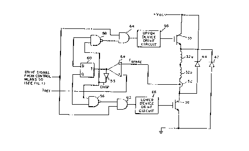
As illustrated in Figure 3, a current sensor 52,
such as one of those hereinabove described, is coupled to the
phase winding comprising series-connected stator pole
windings 32a and 32b. A signal ISENSE proportional to the
sensed phase current is produced by current sensor 52 and is
supplied to the inverting input of a hysteresis comparator
54, such as an LM311 manufactured by National 5emiconductor
Corporation. A commanded reference current waveform IREF is
- 8 - 20~0673
RD-17,680
generated by a reference waveform generator, such as a
function generator (not shown), and is supplied to the non-
inverting input of a comparator 54. The output of comparator
5~ is coupled to an inverter 55 and to one input of each of
two two-input NAND gates 56 and 58. The output signal of
comparator 54 also clocks a T (toggle) flip-flop 60 which is
triggered by a falling or negative edge of the output signal
from comparator 54. Flip-flop 60 generates complementary
logic level output signals at Q and Q. The output signal at
Q is applied to the second input of NAND gate 56, and the
complementary output signal at Q is provided to the second
input of NAND gate 58. The outputs of NAND gates 56 and 58,
respectively, are coupled to one input of each of two two-
input AND gates 62 and 64, respectively. The other input to
each ~ND gate 62 and 64, respectively, is fulfilled by a
drive signal supplied by control means 50. The outputs of
AND gates 62 and 64, respectively, are coupled to a lower
device drive circuit 66 and an upper device drive circuit 68,
respectively. Suitable device drive circuits are well-known
in the art, such as the IR2110 bridge drivers manufactured by
International Rectifier.
In operation, when the sensed phase current,
represented by current ISENSE~ is less than the lower limit of
the hysteresis band, comparator 54 produces a high logic
level signal. Otherwise, if current ISENCE rises above the
upper limit of the hysteresis band, then comparator 54
produces a low logic level signal. The comparator output
signal is supplied to inverter 55 and T flip-flop 60. The
output signal produced by inverter 55 is the CHOP signal. In
particular, when CHOP is a high logic level signal, phase
current chopping is indicated. T flip-flop 60 determines
which of the two switching devices 35 and 38 will be used for
current chopping at any given time. For example, at the
start of the conduction interval of the machine phase
- 9- 201U673
RD-17,680
comprising stator pole windings 32a and 32b, upper and lower
switching devices 35 and 38, respectively, are turned on.
Current builds in the machine phase winding, and when the
sensed phase current exceeds the upper limit of the
hysteresis band, the output signal of compara~or 54 makes a
transition from a high logic level to a low logic level. The
toggle flip-flop is thus triggered by the falling edge of the
output signal of comparator 54.
For example, if the output Q of T flip-flop 60 is
at a high logic level signal indicating that lower switching
device 38 was last used ~or chopping, and current ISENsE rises
above the upper limit of the hysteresis band, then the output
signal of comparator 54 makes a transition from a hi~h to a
low logic level. T flip-flop 60 is triggered by the falling
edge of the output signal from comparator 54 so that the
output signal at Q becomes low and the output signal at Q
becomes high. The low level output signal from comparator 5
is also supplied to inverter 55, causing its output signal
CHOP to become high. The high logic level CHOP signal from
inverter 55 is provided to NAND gates 56 and 58. Since the
output signal at Q from T flip-flop 60 supplied to NAND gate
58 is also high, the output signal therefrom is a low logic
level. This low output signal from NAND gate 58 is inputted
to an AND gate 64, causing a low output signal therefrom
which is supplied to upper device drive circuit 68, thus
turning off upper switching device 35. ~owever, lower
switching device 38 remains conductive while upper switching
device 35 is nonconductive. That is, the logic level signal
at output Q of T flip-flop 60 is low, thus enabling NAND gate
56. The high output signal from NAND gate 56 is suppled to
AND gate 62. Since the drive signal from control means 50 to
AND gate 62 is also high durinq the conduction interval of
the respective machine phase, the output signal from AND gate
62 is high, so that lower switching device 38 remains
- 1 o - 2010673
RD-17,680
conductive. In this way, lower switching device 38 and diode
47 comprise a path for circulation of phase current while
switching device 35 is nonconductive. The drive system
remains in this state until current ISENSE decreases below the
lower hysteresis band limit, at which time the output signal
from comparator 54 becomes low. The CHOP signal, therefore,
becomes low, causing the output signals of NAND gates 56 and
58 to become high. Since the drive signal supplied to these
NAND gates from control means 50 is also high during the
conduction interval of the respective machine phase,
switching device 35 is again turned on and switching device
38 is also turned on. The hereinabove described cycle
repeats during the conduction interval of the respective
machine phase, with the current chopping function alternating
between the upper and lower switching devices. At the end of
the conduction interval, both switching devices 35 and 38 are
turned off, and current flows through diodes 44 and 47 back
to the DC source. Hence, at this commutation point, there is
approximately a voltage
20 -VDC across the phase winding which causes the phase current
to decrease quickly to zero.
Figure 4 graphically illustrates a DC link ripple
current waveform for a SRM drive employing the current
chopping strategy of the present invention. When both
switching devices are conductive, DC link ripple current is
positive; and, when one switching device is nonconductive, DC
link ripple current is zero. As compared with the
conventional current chopping strategy for which the ripple
current waveform is illustrated in Figure 2, the PWM chopping
frequency is substantially lower, and there is a reduction of
over 65% in ripple current. ~herefore, the size of capacitor
40 can be advantageously decreased.
Advantageously, by alternating chopping between
switching devices of each respective machine phase during the
- 11 - 2010673
RD-17,680
conduction intervals thereof, the conduction and switching
losses are balanced between these devices. Power
dissipation, therefore, is likewise shared. However, in
accordance with an alternative embodiment of the present
invention, only one of the switching devices is used for
current chopping~ By way of example, as shown in Figure 5,
upper switching device 35 is the chopping device, while lower
switching device 38 remains on throughout each conduction
interval of the respective machine phase. During the
conduction interval of the respective machine phase, when
current ISENSE exceeds the upper limit of the hysteresis band,
the output signal of comparator 59 is a low logic level, thus
disabling AND gate 64 and turning off upper switching device
35. However, since the drive signal from control means 50 to
lower device drive circuit 66 is a high logic level signal
during the conduction interval of the respective machine
phase, lower switching device 38 remains on. Phase current,
therefore, circulates in the path provided by lower switching
device 38 and flyback diode 47. The upper switching device
is again turned on when current ISENSE decreases below the
lower hysteresis band limit. This process repeats with upper
switching device 35 chopping and lower switching device 38
remaining on throughout each conduction interval.
By using the current chopping strategy of the
present invention, switching frequency is advantageously
reduced. This is the result of phase current circulating
through the conducting switching device and corresponding
flyback diode, while the chopping device is nonconductive.
In particular, in a conventional chopping scheme, when both
switches are turned off, current is returned to the DC source
via flyback diodes. This effectively results in a voltage
-VDC across the phase winding, causing current to decrease
rapidly. By way of contrast, with current circulating
according to the present invention, current is not returned
- 12 - 2010673
RD-17,680
to the DC source, and the effective voltage drop across the
phase winding is the sum of the voltage drops across the
conducting switching device and the corresponding flyback
diode. Since this effective voltage drop is small compared
with voltage -VDC, the circulating current decreases more
slowly, thereby decreasing the chopping frequency. A lower
chopping frequency results in lower switching losses and
hence lower device junction temperatures.
While the preferred embodiments of the present
invention have been shown and described herein, it will be
obvious that such embodiments are provided by way of example
only. Numerous variations, changes and substitutions will
occur to those of skill in the art without departing from the
invention herein. Accordingly, it is intended that the
invention be limited only by the spirit and scope of the
appended claims.