Note : Les descriptions sont présentées dans la langue officielle dans laquelle elles ont été soumises.
2011102
In microprocessor based systems such as personal computers and the like
the video hardware for controlling a video display (monitor) comprises a video
adaptor which interfaces the video commands issued by the CPU to the monitor.
One of the most popular video adaptors used in personal computers is the video
graphics array (VGA) manufactured by International Business Machines, Armonk,
New York. The VGA has gained such wide popularity and use that several
manufacturers provide hardware that emulates the VGA and numerous software
producers have developed software that utilize the VGA to produce the video
output.
A block diagram of the VGA is shown in Fig. 1. The VGA comprises the VGA
chip or controller 20, memory 10 which functions as the frame buffer and the
storage of fonts and the like and the digital to analog converter (DAC) 30
referred to
sometimes as the pallate chip which functions as the color lookup table for
the
color display as well as the driver for the monitor 40. VGA chip 20 is
connected to
the CPU through the PC bus. The CPU transmits to the VGA chip which receives
the video commands regarding what information to display and not to display.
To
generate a display the CPU instructs the VGA chip 20 to display a certain set
of
data. Upon receipt of commands from the CPU, the VGA sends the required
instructions - if it is in the text mode the 16-bits containing character
attributes, if it is
in the graphics mode the pixel information - to the memory 10 to generate the
frame
buffer image. The frame buffer image is then transmitted back to the VGA chip
which forwards one pixel at a time the contents of the frame buffer to the DAC
30.
The 4-bit pixel code (4 bits for 16 colors, 8 bits for 256 colors) transmitted
to the
DAC 30 is used to determine the color of the pixel through the color lookup
table.
Once the color of the pixel is determined through the lookup table, the
digital
signals are converted to analog signals and output to the monitor 40 for
display.
The contents of the frame buffer are read and transferred to the DAC 30 sixty
(60)
times a second in order to refresh the display on the monitor display 40. Due
to the
extreme popularity of the VGA, computer manufacturers have attempted to design
MEM/Idr 1 82225.P080
2011102
video hardware and software that are backwards compatible with the VGA, such
that popular software programs that are compatible only with the VGA will work
on
the more recent versions of computers.
However, a new feature found in the many of the newer multitasking
computers, referred to as windowing, has made the problem of compatibility
with
the VGA even more difficult. Software programs which provide this feature
include
"Microsoft Windows", developed by Microsoft Corporation, Redmond, Washington
and "Presentation Manager", developed by International Business Machines,
Armonk, New York. In a windowing environment, the screen may be divided up
into a plurality of areas, each referred to as a window, in which different
processes
may be run simultaneously. For example, in a first window an accounting
program
may be operating while in a second window a drawing program may be running.
The user of the computer has the ability to switch from window to window to
operate the separate processes. The graphics portion of windowing system which
contains the display is typically a separate program which receives as input
the
parameters designating the different windows on the screen and the
applications
that are to operatQ in each of the windows, such that when the application
program
indicates the display is to change that information is sent to the windowing
system
which takes the video information and massages the data, i.e., compresses the
size
of the data as well as clips and trims the data in view of the window and its
relations
to other windows displayed, and outputs the massaged data to the frame buffer
of
the monitor for display. Computer hardware developers have tound however, that
the VGA will not wortc in the window environment and have been unable to take
a
VGA generated display and allocate it to a portion of the screen. If a VGA-
based
process, that is a process which utilizes the VGA to generate its video
output, is to
be executed, the applications running under the windowing system must be
suspended and saved and the screen blanked so that the VGA process can display
its video image.
MEM/Idr 2 82225.P080
2011102
To overcome this problem there have been attempts to develop VGA
emulation software that is compatible with the windowing system so that VGA-
based processes are displayable within the windowing system. However, software
emulators require a large amount of CPU overhead and dramatically slow down
the time required to generate a display. Tests have shown that to generate a
video
image through a software emulator may to be up to 83 times slower than the
time
typically required to generate the same image in a non-windowing environment.
The method and apparatus of the present invention seeks to overcome these
problems by providing an interface between the VGA and a non-VGA compatible
erwironment such as the windowing environment and system software such that
VGA based applications may be displayed in the incompatible environment on a
real time basis.
Furthermore, it has been found that the method and apparatus of the present
invention may be utilized to perform real time comparisons of large blocks of
raster
data, such as seismic and geological data, radar data and video imaging data,
data
such as the data employed in image processing. Currently in such applications
when two blocks of data are to be compared, the comparisons are performed by
software which compares the blocks of data on a bit by bit basis. This is
quite time
consuming and makes real time processing of the data difficult except on
large,
powerful, main frame computers. The method and apparatus of the present
invention provides a real time capability for the comparison and detection of
changes in raster data without utilizing powerful main frame computers.
MEM/Idr 3 82225.P080
zo~~~oz
It is therefore an object of the present invention to provide an interface
between a video adapter and an incompatible graphics display environment such
that the output of the video adapter can be displayed within the incompatible
graphics display environment on a real time basis.
It is an object of the present invention to provide an interface between a
video adapter such as the vertical graphics array (VGA) video adapter and an
incompatible graphics environment, such as a windowing system, wherein VGA-
based applications may be displayed and output through the windowing system on
a real time basis.
It is furthermore an object of the present invention to provide a method and
apparatus that permits real time comparisons of and detections of changes
between blocks of raster data.
In the method and apparatus of the present invention the data, i.e. raster
data, is stored in memory. During the process of storing the data in memory,
the
data currently in the memory is read on a bit by bit basis and compared to the
bits
to be written into the same location in memory. Preferably a circuit such as a
simple exclusive OR or comparator circuit is used to perform the comparison.
If the
data read from a certain location and the data to be written to that same
location
are not the same, the discrepancy and location of the discrepancy is noted in
a
separate area of memory to be used for subsequent analysis and the data to be
written to that location is immediately written into the memory. Preferably,
the type
of memory to be used is a dynamic random access memory (DRAM) because the
DRAM performs the read of the data currently in memory and the write of the
new
data into memory during one memory cycle.
MEM/Idr 4 82225.P080
2011 102
The method and apparatus of the present invention is particularly
applicable to the video graphics environment wherein the current bit or raster
image contained in the frame buffer is compared to the updated raster image
and the data changes are noted on a pixel by pixel basis using the method
and apparatus of the present invention. Utilizing the information gathered on
the changed pixels, the video display need only update the changed data,
thereby minimizing the amount of data to be transferred and increasing the
speed of the system.
In a preferred embodiment the method and apparatus of the present
invention is employed to provide an interface between a video adapter such
as a video graphics array (VGA) and a video display system incompatible with
the video adapter such as a windowing system whereby the video output
generated by the video adapter is translated and input to the video display
system for generation of the display in real time.
In one aspect, the present invention provides in a computer graphics
system for the generation and display of raster data images comprising a
central processing unit (CPU) coupled to a memory means, said CPU further
being coupled to a display means for the display of a raster data image, said
raster data image comprising a plurality of pixels, each pixel identified at
an
X-Y coordinate location within the raster data image, a method for comparing
a first and a second raster data image in real time wherein a pixel at a
specific
X-Y coordinate location in the second raster data image is compared to a
pixel at the specific X-Y coordinate location in the first raster data image
as
°e
_5_
2011102
each pixel of the second raster data image is generated, said method
comprising the steps of: writing the first raster data image into memory such
that each pixel data representative of a pixel at a predetermined X-Y
coordinate location in the image is written to predetermined memory location;
receiving a pixel data of the second image being generated, said pixel data
representative of a pixel located at a specific X-Y coordinate location in the
second raster data image; reading the first raster data image stored in
memory to retrieve pixel data corresponding to a pixel in the first raster
data
image at the specific X-Y coordinate location; inputting to a comparator
circuit
the pixel data read from memory and the pixel data of the second raster data
image received; and if the comparator output indicates that the pixel data
read from memory and the pixel data of the second raster data image are not
the same, recording the identification of the X-Y coordinate location of the
pixel data to indicate that the pixel data has changed.
.~--.
a-
2011).2
The objects, features and advantages of the method and apparatus of the
present invention will be apparent from the following detailed description of
the
invention in which:
Fig. 1 illustrates the VGA video adapter system.
Fig. 2a and 2b illustrate one embodiment of the system of the present
invention in which large amounts of memory containing raster data may be
compared in real time.
Fig. 3 illustrates a block diagram depicting another embodiment of the
system of the present invention, a video system interface, as it functionally
relates
to the VGA video system and a windowing system.
Fig. 4 is a block diagram of the video system interface of the present
invention.
Fig. 5 illustrates the formation of dirty regions from dirty pixels in the
video
system interface of the present invention.
Figs. 6a and 6b is a flow chart illustrating the process steps performed by
the
programmable dirty region central of the new system interface of the present
invention to determine dirty pixel regions.
MEM/Idr 6 82225.P080
2011.42
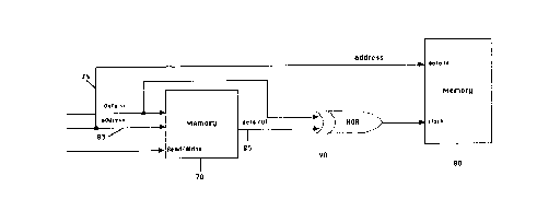
Referring to Fig. 2a the system of the present invention comprises a first
memory 70, exclusive OR circuit (XOR) 90, and a second memory 80. The first
memory 70 may be any memory used to store large amounts of raster data such as
digital video image or radar image data. Data to be written into memory is
input via
the data line 75 and the address the data is to be written to is input via
address line
83. The raster data is consistently written to the same locations in memory
such
that like data to be compared, e.g. a pixel at a specific X-Y coordinate
location, is
always written to and read from the same address in memory. Thus a direct
correlation is established between each pixel location and a memory location
where the pixel information is stored. Prior to writing the data, (herein
referred to as
the "incoming data,") into memory, a read operation is performed to read the
contents of the address the data is to be written to and the data (herein
referred to
as the "current data" is output on the data out line 85 to a first input read
pin of XOR
circuit 90. The incoming data on line 75 is input to a second input pin of XOR
90
and the current data and incoming data are compared. The output of the XOR
circuit 90 indicates whether the incoming data and the current data is the
same. If
the output of XOR circuit 90 indicates that the data is not the same, the data
memory address on line 83 is clocked into a second memory 80 for storage.
Immediately after the current data is read from memory 70, the incoming
data is written into memory at the address on address line 83. Preferably the
memory write operation is performed concurrently with the XOR operation to
minimize the number of clock cycles required to perform the comparison of data
and the storage of data into memory. Thus the steps of reading the data from
memory and comparing the current data to the incoming data preferably takes
place in one memory cycle. During the second memory cycle the incoming data is
written into memory 70 and concurrently with that cycle the address of the
memory
location is stored in memory 80 if the current data and the incoming data are
not
the same. Although it is preferred that the information stored in memory 80 is
the
MEMIId~ 7 82225.P080
20ii1.~2
memory location, other information which identifies the data, such as the X-Y
coordinate location of the corresponding pixel on the display, may be used.
The process and apparatus can be expanded to read, compare and write
multiple bits during the same memory cycle. If the memory 70 is a 32 bit wide
memory, the 32 bits of data would be input over 32 data lines to the 32 data
input
pins of the memory 70 which would write the 32 bits into memory within one
cycle.
Prior to writing the data into memory, the 32 bits of the current data would
be read
and output through the 32 data output pins to 32 input pins of one or more
comparator circuits (depending upon the number of inputs to each comparator
circuit), which would simultaneously compare the 32 bits of incoming data and
current data and output data indicative of the bits which differed and this
information would be stored in memory.
Fig. 2b illustrates the preferred configuration of this embodiment of the
present invention. Although any type of read/write memory may be used, it is
preferred that the system of the present invention employs Dynamic Random
Access Memory (DRAM). The DRAM offers a single cycle memory operation
referred to as the read-modified-write memory cycle (RMW). In the RMW, prior
to
writing data, the old data currently stored in the memory is read and output
from
memory on the data out line . This memory operation is preferred because the
data
currently stored in the memory is read out and the new data is written into
memory
within one memory cycle, and therefore, the process of reading the current
data
from memory, comparing the incoming data and the current data and writing the
incoming data into memory can be performed within one memory cycle. This
embodiment is particularly useful when examining digital video images or other
types of raster data to determine changes in the data. An illustration is the
processing of radar signals wherein it is important to note the movement of
"blips"
or images representative of aircraft or the like among the radar signals. This
embodiment is also useful to determine changes in seismic or geological data
MEM/Idr 8 82225.P080
2011102
wherein the majority of information remains the same with minor deviations in
the data.
Furthermore, this embodiment may be utilized in the area of digital
video imaging wherein real time updating of rasterized or digital video images
is achieved by transmitting only those portions of the image that have
changed since the last time the image was transmitted. A bottleneck in the
digital video imaging process is the time required to transmit the raster data
representative of the video image from an input means to an output means,
such as from the CPU to the frame buffer or from the origin to the final
destination of the video image, for example, across telephone lines or
satellite
links as is frequently done in video teleconferencing. Thus it is preferred
that
the amount of data that is needed to transmit is minimized. This is often done
through data compression techniques wherein the video data is compressed
prior to transmission and subsequently expanded after receipt of the
transmission. However, the process may be simplified and the transmission
time minimized by transmitting only the data representative of the portions of
the image changed since the last transmission. The increase in transmission
speed is significant because in most applications the amount of change
occurring in a video image when the image is frequently updated is a small
percentage of the total image.
One application, where the system of the present invention has been
particularly useful, illustrated in part by Fig. 3, is to provide an interface
-9-
2011 102
between a video adapter such as a video graphics array (VGA) and a video .
system incompatible with the video adapter, such as a windowing system.
A computer program VGA based application 120 communicates
through the CPU the video data to be displayed to the VGA subsystem 130,
and in particular the VGA controller chip. The output of the VGA controller
chip, which in a typical VGA system is output through a digital to analog
converter (DAC) and to a display monitor 160, is input to the video interface
140 of the present invention. The video interface 140 converts the VGA
output data into raster data which is compatible with and can be interpreted
as input to the windowing system 150. The windowing system 150 upon
receiving the raster data then massages the data to display it in the proper
window of the display monitor 160. A more detailed block diagram of the
video interface 140 is illustrated in Fig. 4.
Referring to Fig. 4, the VGA interface comprises VGA controller chip
220, Pixel Packer 170, Timing Control 180, Frame Capture RAM 190, Dirty
pixel comparator 195, Programmable Dirty Region Control 200, Bus ,
interfacellookup table 210 and Dirty region storage 230. The timing control
180 controls the timing of all the components of the video interface and
coordinates the timing of the video interface with the VGA and the windowing
system. The timing control 180 controls the timing of the captures, the
setting
of the line length, retrace length, the number of lines and sends out an
interrupt to the CPU after the capture and dirty pixel processing is complete
to
indicate that data is to be transferred to the windowing system. Timing
-10-
2011 102
control 180 receives timing signals from the VGA 220, such as the horizontal.
synchronizing signal, vertical synchronizing signal, blank signal and the
clock
signal, and provides the timing signals for the pixel packer 170, frame
capture
RAM 180, dirty pixel comparator 195, programmable dirty region control 200
and dirty region storage 230. The timing control 180 also contains several
counters which are used in conjunction with the timing signals received from
the VGA 220 to Calculate the memory address in frame capture RAM 190 the
pixel information output by pixel packer 170 is to be written to such that a
pixel from a particular X-Y location is consistently written to the same
address
in the frame capture RAM.
When data is to be displayed or data currently displayed is to be
changed or updated, the VGA-based application program indicates to the
CPU the video data to be displayed. This information is transferred in VGA
format to the VGA controller chip 220 which is the same VGA controller chip
used in VGA video adapters presently available. The VGA controller 220
then performs the standard functions to generate the raster image. Once the
raster image is generated, the raster data is ,
- 1 Oa -
X011102
transferred out of the VGA controller chip 220 pixel by pixel. In a standard
VGA
system, this information would be output to a DAC containing a color lookup
table
which would generate the proper control signals for output for display on the
monitor. However, in this embodiment of the video interface of the present
invention, the output of the VGA controller chip 220 is periodically
"captured" for
transmission to the Frame Capture RAM 190. Thus, for output, the pixel data
typically a 4-bit word or nibble, is sent to the memory 190 herein referred to
as
frame capture RAM, for temporary storage.
Preferably, the data output by the VGA controller chip 220 is captured at a
predetermined frequency. For example, the current raster image may be output
by
the VGA controller chip 220, "captured" and transferred to the frame capture
RAM
190 once every ten seconds. This permits the control of the frequency of
updates
to the raster image displayed and can be increased or decreased according to
the
application outputting the raster data to accommodate applications which
continuously change the raster image and those which change the raster image
less often.
In order to minimize the number of memory cycles for transferring the raster
image from the VGA to the frame capture RAM 190, it is preferred that the
pixel data
is sent in blocks of data comprising multiple pixels. Typically the block size
is set to
equal the width of the RAM 190 such that one row of data is written during
each
memory cycle. This is accomplished using pixel packer 170. Pixel packer 170
receives the pixel data from VGA controller 220 and stores the information
until the
amount of pixel information stored equals the size of the output block of
data. The
block pixel data is then output from pixel packer 170 and written to RAM 190
in one
memory cycle. Preferably pixel packer 170 comprises a mufti-bit shift register
or
latch n-bits long wherein "n" equals the width of the RAM 190 such that pixel
data is
written in RAM one row at a time.
MEMlldr 1 1 82225.P080
2 01. ~.1. 0 .2
The frame capture RAM 190 is preferably a DRAM with the read-modified-
write mode enabled such that data may be read out of memory and written into
memory within one memory cycle . Thus, within a single memory cycle, the
current
data stored in the DRAM may be read from memory, the incoming data to the RAM,
that is the data output by pixel packer 170, may be written into memory and
the
current data and the incoming data can be compared using the dirty pixel
comparator circuit 195 to determine if the data has changed. Preferably dirty
pixel
comparator circuit 195 compresses a multiple bit XOR circuit such as the one
described above with respect to Fig. 2b. The information indicating the
locations of
the pixels have changed, referred to as the dirty pixel data, is transferred
to the
programmable dirty region control circuit 200. The programmable dirty region
control circuit 200 analyzes the data that has been changed and determines the
groups or regions of raster data ("dirty regions") to be transmitted to the
window
system for updating tha displayed raster image. Once the dirty regions have
been
determined by programmable dirty region control 200, the X-Y coordinate limits
of
the dirty regions are stored in dirty region storage memory 230. Although
dirty
region storage memory is shown as a separate memory from the frame capture
RAM 190, it may physically be on the same memory chip as the frame capture
RAM 190 in order to conserve space.
The programmable dirty region control 200 uses a predetermined set of
control parameters to analyze the dirty pixel data and its location in
relation to one
another and group the dirty pixel data into regions, referred to as "dirty
pixel
regions", according to its X-Y coordinate location within the raster image.
The control parameters used to determine the dirty pixel regions that are to
be updated on the display vary according to the sophistication and
optimization of
the system desired. The windowing system adds significantly to the system
overhead, slowing down the processing speed of the system. Thus, it is
desirable
that the number of system calls to the windowing system is minimized. The
amounts of data transmitted between components in the system also impacts the
MEM/Idr 12 82225.P080
2011102
overall processing speed of the system. Therefore, it is also desirable to
minimize
the amount of data to be transferred to the windowing system. To optimize the
speed of the system, for example, the parameters which control programmable
dirty
region control 200 can be set such that each region comprises a single dirty
pixel
or that any one dirty region is determined comprising all the dirty pixels of
the video
image. However it is preferred the programmable dirty region control 200 is
programmed to form dirty regions which balance the advantage of issuing as few
commands as possible to the window system and minimizing the amount of video
data that has to be transferred and processed by the windowing system. The
parameters used to control the programmable dirty region control circuit
preferably
comprise the maximum size of a dirty region in the horizontal direction
(XMAX), the
maximum size in the vertical (YMAX), the minimum number of clean pixels
horizontally between dirty regions (XCLEAN) and the minimum number of clean
pixels vertically between dirty regions (YCLEAN). XMAX and YMAX limit the size
of
a dirty region of a raster image. This is to prevent the transmission of an
entire
raster image in the instance of a shape, such as a full screen cross-hair,
which may
extend over a large portion of the screen but only a small number of pixels in
limited areas of the screen are affected. The minimum clean parameters, XCLEAN
and YCLEAN limit the number of regions and thus the number of calls to the
?0 windowing system.
Preferably, the programmable dirty region control 200 hardware comprises a
state machine or microprocessor which analyzes the data using parameters
provided. The parameters may be preset or they may be adjusted according to
the
type of application. For example the size of the dirty regions may be
decreased if it
is found that the ratio of the number of dirty pixels in the region to the
total number
of pixels in the region is small. Furthermore the parameters may be altered
dynamically consistent with the type of video output generated. The processor
may
analyze the video output concurrently with the analysis of dirty pixels and
determine the optimum parameters, e.g. dirty pixel region size and number of
regions, for the video data.
MEMAdr 1 3 82225. POGO
2~~11~~
An illustrative process for analyzing dirty pixel data is presented in the
flow
charts of Fig. 6a and Fig. 6b. This exemplary process permits one region per
scan
line with the X coordinate limits of the regions determined by the rightmost
and
leftmost dirty pixels within each region. The number of scan lines which
comprise
each region is limited to a predetermined maximum number of scan lines. In
addition, if a predetermined number of scan lines do not contain dirty pixels
(i.e. the
scan lines comprise "clean pixels"), the dirty region will be closed at the
last scan
line containing dirty pixels and a new dirty region will be formed at the next
occurrence of a dirty pixel. The resulting regions after analysis of the dirty
pixel
using this process is illustrated in Fig. 5. Fig. 5 is a simplified drawing of
a raster
image showing dirty pixels at the pixel locations marked with an "X". For
purposes
of illustration, assume that a region can not be larger than five scan lines,
and if
there are three clean scan lines (i.e., no dirty pixels), the current dirty
region is
closed and a new dirty region is opened. According to the above parameters,
three
dirty regions 293, 295, and 298 would be defined.
Referring to the flow chart of Fig. 6a, at block 300 the X and Y counters are
initialized and the dirty pixel count is set to zero. The X-Y counters are
used to
keep track of the X,Y coordinate location of current pixel being analyzed, and
the
dirty pixel count keeps record of the number of dirty pixels and may be used
to
control the size of the dirty regions. If the capture of the raster image
began at the
beginning of the image, that is immediately after the retrace signal, the X
and Y
counters would be set to zero. However, if the capture began at another
portion of
the raster image, e.g. at the 20th scan line, the X counter would be to zero
and the
Y counter would be initialized to 20.
At block 305 the dirty region pointer used to point to the data structure of
"open" dirty pixel region is set. At block 310 the current pixel as indicated
by the X
and Y counter is analyzed to determine whether the pixel is dirty. If the
pixel is
dirty, at block 315, the dirty region pointers and counters, STARTX, STARTY,
MEMlldr 14 B2225.P080
201112
ENDX, ENDY,are set to track the beginning of the dirty region. Thus, the dirty
region is defined by a STARTX, STARTY indicating the upper left hand corner of
the dirty region, and ENDX, ENDY indicating the bottom right hand corner of
the
dirty region. Initially, STARTX and ENDX are set to the current X coordinate
location as indicated by the X pointer, and STARTY and ENDY are set to the
current Y coordinate lacation as indicated by the Y pointer. In addition, the
count of
dirty pixels is started by having a value of one to track the total number of
dirty
pixels per capture image.
Once the STARTX, STARTY, ENDX, ENDY parameters have been adjusted,
at block 320, the location of the dirty pixel is examined to determine whether
the
end of a scan line has been reached. If the end of the scan line has been
reached,
at block 325, the pixel location is examined to determined whether the last
row of
the capture has been reached. li the last row of the capture has been reached,
at
block 330 the analysis of the current video image is complete. If at block 325
the
bottom of the screen has not been reached, at block 330 the X and Y counters
are
adjusted such that Y counter is incremented by one, and the X counter is reset
to 0
whereby the counters point to the beginning (leftmost pixel) of the line one
line
below the scan line just analyzed. If at block 320 the end of the row has not
been
reached, then at block 335 a value of one is added to the X counter indicating
that
the next pixel to the right of the pixel just examined is to be analyzed.
At block 340, the next pixel is analyzed to determined whether it is a dirty
pixel. If it is a dirty pixel, at block 345 the system determines whether the
current X
location is to the left of the current STARTX location. If the current X is to
the left of
STARTX, at block 350 the STARTX parameter is adjusted to the value equal 1o
the
X counter. If at block 345 the current X location is not to the left of the
STARTX,
then at block 355 it is determined whether the current X location is to the
right of the
ENDX location. If it is beyond the region as currently defined by ENDX, then
at
block 360 ENDX is adjusted to be equal to the current X location. Similarly,
at
block 365, the current Y location is compared to STARTY and ENDY to determine
if
MEM/Idr 1 5 82225.P080
20.1102
it is within the current Y boundaries of the open dirty region. Thus at block
365, the
current Y location is compared to the ENDY location. If the current Y location
is
below ENDY at block 367 a second check is performed to determine whether the
open dirty region comprises the maximum number of scan lines allowed (YMAX).
If
the open dirty region comprises the maximum number of scan lines at block 368
the dirty region is closed and a new dirty region is opened whereby STARTX,
ENDX are set to equal the X counter and STARTX and ENDY are set to equal the Y
counter. If the open dirty region does not comprise the maximum number of scan
lines at block 370 ENDY is adjusted to be equal to the current Y location.
After the limits of the region, that is the STARTX, STARTY, ENDX and ENDY
parameters, have been adjusted as necessary the dirty count is increased for
the
region and the process returns to block 320 where the steps are repeated again
until the end of the capture has been reached.
If at block 340 the current pixel being examined is not dirty, at block 375
the
current Y location is examined to determine whether the Y location is greater
then
the ENDY location of the current dirty region plus the minimum clean Y
(MINCLEANY) parameter that is preset in the system. The minimum clean Y
parameter provides the minimum number of continuous clean scan lines between
dirty regions. Therefore if the minimum number of continuous clean scan lines
are
found the open dirty region will be closed and any subsequent dirty pixels
found
will be part of a new dirty region. Thus if the scan line at the current Y
location
which is clean is currently greater than the sum of ENDY plus MINCLEANY, at
block 380 the open dirty region is closed and a new dirty region is opened. At
blocks 385, 390, 395, 400, 405 the X,Y counters are incremented to point to
the
next pixel location to be examined and the process continues at block 310,
whereby the process continues until the bottom of the last row of the capture
has
been examined. This coordinate boundaries of each dirty pixel region is
transmitted to the windowing system.
MEMIId~ 1 6 82225. POGO
201~.~~2
Once the programmable dirty region control 200 has finished analyzing the
dirty pixel data and the dirty pixel regions have been formed, an interrupt
signal is
sent to the CPU through the bus 230 to notify the CPU that there is data to be
output to the windowing system. The CPU then reads the dirty region
information
containing the X Y boundaries of the dirty regions (STARTX, STARTY, ENDX,
ENDY) and uses the boundaries of each region to read ,through commands sent to
the programmable dirty region control 200, the corresponding frame capture RAM
locations containing the raster data within the boundaries of the region. In
response to the memory read regions, the raster data is output through the bus
interface/table lookup 210 onto the bus 230 to the windowing system, whereby
the
windowing system massages the data within the dirty pixel region and outputs
the
data to the proper window of the display.
When the pixel data is read from the frame capture RAM, the data is output
along bus 240 to the lookup table in bus interface /lookup table 210. In the
lookup
table, the color code for each pixel is converted to the proper format
acceptable by
the windowing system.. This is done by a simple lookup table wherein the
current
color code output from the frame capture RAM indexes the location in the table
and
outputs the code read from that indexed location. In addition, it the pixel
data is
represented by a 4-bit code, such as VGA format data, and the windowing system
requires an 8-bit code, the lookup table changes the code from a 4-bit code to
a
compatible 8-bit code. Preferably the color lookup table comprises two
identical
lookup tables each indexed by a four bit number. This is to accommodate the
incoming data from the frame capture RAM 190 which is transmitted in a 4
bit/pixel
format. Thus when the bus interface/color lookup receives 8 bits of raster
data
corresponding to two pixels, the lower 4 bits index to the first color lookup
table and
the higher 4 bits index to the second lookup table to translate the raster
data.
While the invention has been described in conjunction with the preferred
embodiment, it is evident that numerous alternatives, modifications,
variations and
uses will be apparent to those skilled in the art in light of the foregoing
description.
MEM/Id~ 1 7 82225.P080
2011102
In particular it is evident that the VGA interface described may also be used
in
conjunction with other video systems including systems which do not provide
for a
windowing capability. In addition it is evident that the VGA interface may be
adapted to be provide a system interface for other video adapters such as the
EGA
and Hercules video adapters.
MEM/Idr 1 8 82225.P080