Note : Les descriptions sont présentées dans la langue officielle dans laquelle elles ont été soumises.
20111~
SEMICONDUCTOR LASER DEVICE
The present invention relates to the structure of a
semiconductor laser, and more particularly to a high-power
semiconductor laser device necessary to apparatuses for
consumer use.
A prior art laser of this kind will be described
hereinbelow in detail.
It is an object of the present invention to provide
a semiconductor laser device of the phased array type, in
which device phase-locked oscillation can take place all over
a stripe region, independently of which of a CW operation and
a pulsed operation is performed.
In order to attain the above object, in a
semiconductor laser device according to the present invention,
a current which does not contribute to Gscillation, flows on
both sides of a stripe region, that is, dummy stripes or
regions are provided on both sides of the stripe region.
According to the present invention, dummy stripes
are provided on both sides of a stripe region. Hence, even in
a case where a CW operation is performed and thus it is
necessary to take the generation of heat into consideration,
the temperature distribution in the stripe region is made
uniform, and thus stable phase-locked oscillation can take
place all over the stripe region. ~s a result, a laser beam
which is excellent in coherency, is emitted even when the CW
operation is performed.
.
... .. .
..: -
';'~ ' :
. . .
: . , . ' ' ,: . - '
~" 20111~
In accordance with one aspect of the invention there
is provided a semiconductor laser device, comprising: a
semiconductor substrate; a semiconductor structure, including
an active layer, provided on the substrate; a first electrode
provided on a side of the substrate; a second electrode formed
on a side of the semiconductor structure not adjacent the
subs~rate; a resonant cavity; an oscillating stripe region
which includes a plurality of oscillation stripes
substantially parallel to the direction o~ cavity length, with
each indiYidual stripe in said plurality of oscillation
stripes also being substantially parallel to each of the other
individual oscillation stripes, so that phase-locked
oscillation can be generated at adjacent oscillation stripes,
the oscillation stripe region being provided at a central part
of the device; and dummy regions for flowing a current which
does not contribute to laser oscillation, disposed in
proximity to the oscillation stripe region, outside of the
oscillation stripe region, at both sides thereof.
Fig. 1 is a schematic diagram showing the pulsed
operation of a conventional phase-array semiconductor laser
device.
Fig. 2 is a schematic diagram showing the CW
operation of the conventional phased-array semiconductor laser
device.
2S Fig. 3A is a graph showing the temperature
distribution in the conventional phased-array semiconductor
laser device.
, .
- 20111~5
Fig. 3B is a graph showing the temperature
distribution in an invention semiconductor laser device
provided with dummy stripes.
Fig. 4 is a plan view showing a representative
structure of an inventive semiconductor laser device, that is,
showing the first embodiment of semiconductor laser device
according to the present invention.
Fig. 5A is a sectional view taken along the line
A-A' of Fig. 4.
' lO Fig. 5B is a sectional view taken along the line
B-B' of Fig. 4.
~, Fig. 6 is a plan view showing the second embodiment
o~ a semiconductor laser device according to the present
invention.
Fig. 7 is a sectional view showing the second
embodiment.
Fig. 8 is a plan view showing the third embodiment
of a semiconductor laser device according to the present
invention.
Fig. 9 is a sectional view taken along the line A-A'
of Fig. 8.
Fig. 10 is a plan view showing the ~ourth embodiment
of a semiconductor laser device acaording to the present
invention.
Fig. ll is a sectional view taken along the line
A-A' o~ Fig. 10.
.
;. . .
2 ~
Fig. 12 is a plan view showing the fifth embodiment
of a semiconductor laser device according to the present
invention.
Fig. 12A is a sectional view taken along the line
S A-A' of Fig. 12.
Fig. 13 is a plan view showing the sixth embodiment
of a semiconductor laser device according to the present
invention.
Fig. 13A is a sectional view showing the sixth
embodiment.
Fig. 14 is a plan view showing the seventh
embodiment of a semiconductor laser device according to the
present invention.
Fig. 14A is a sectional view taken along the line
A-A' of Fig. 14.
Fig. 15 is a graph showing relations between a ratio
of the gain at a stripe to the gain at an interstripe portion
and a threshold gain in a case where the (N+l)th order mode is
not cut off.
Fig. 16A is a graph showing the spatial distribution
of the amplitude of electric field due to the first-order
mode.
Fig. 16B is a graph showing the spatial distribution
of the amplitude of electric field due to the N-th order mode.
Fig. 16C i9 a graph showing the spatial distribution
of the amplitude of electric field due to the ~N+l)th order
mode.
-4-
. , .
:, :
, - . ,
''~ ' ~ : ,
.' ' .
20111~
Figs. 17A, 17B and 17C show far field patterns in
the first order mode, the N-th order mode and the (N+l)th
order mode, respectively.
Fig. 18A is a sectional view showing a semiconductor
laser device which is used as the mother structure of the
eighth embodiment of a semiconductor lassr device according to
the present invention.
Figs. 18B and 18C show the refractive index
distribution and gain distribution in the semiconductor laser
device of Fig. 18A, respectively.
Fig. l9A is a sectional view showing a semiconductor
laser device which is used as the mother structure of the
ninth embodiment of a semiconductor laser device according to
the present invention.
Figs. l9B and l9C show the refractive index
distribution and gain distribution in the semiconductor laser
device of Fig. l9A, respectively.
Fig. 20A is a sectional view showing a semiconductor
laser device which is used as the mother structure of the
tenth embodiment of a semiconductor laser device according to
the present invention.
Figs. 20B and 20C show the refractive index
distribution and gain distribution in the semiconductor laser
device of Fig. 20A, respectively.
The high-power semiconductor laser device is used as
a light source for a second harmonic generation, and is
required to generate oscillation having a single transverse
~t~
" ,. .
:. : . '
' ' '
~ 20111~5
mode and to emit a high-power laser beam capable of forming a
single lobed for field pattern. The output power of the laser
device is determined by the optical power density at the facet
thereof. That is, in order to increase the output power, it
is required to enlarge the size of the light spot at the
facet. As described in an article by ~.R. Scifres et al.
(Electronics Letts, Vol. 19, No. 5, 1983, pages 169 to 171),
the output power can be increased by using a plurality of
oscillation stripes (hereinafter simply referred to as
"stripes") parallel to the direction of cavity length. In a
case where the semiconductor laser is operated under pulsed
current and thus it is unnecessary to take the generation of
heat into consideration, all the stripes are equal in phase of
oscillation to each other. Fig. 1 shows a laser beam in a
case where the semiconductor laser is operated in a pulsive
manner.
While, in a case where the semiconductor laser
performs a CW (continuous wave) operation and thus it is
~I necessary to take the generation of heat into consideration,
phase-locked oscillation takes place only at central stripes
and does not take place at outer stripes, as shown in Fig. 2.
Thus, the coherency of an emitted laser beam is lowered. This
phenomenon will be explained below, with reference to Fig. 3A.
Now, let us consider a case where the semiconductor laser
performs the CW operatlon. As shown in Fig. 3A, the
temperature of a central portion of a stripe region i8 greatly
increased, but the temperature of a peripheral portion of the
i`
. .
~: .
E
. .
1 .
, .
20111~
stripe region is lower than the temperature of the central
portion, because heat conducts from the peripheral portion to
the outside of the stripe region. That is, non-uniform
temperature distribution is generated in the stripe region. As
a result, an optical property is not uniform in the stripe
region. Thus, it is impossible to generate phase-locked
oscillation all over the stripe region.
Embodiments of the present invention will be
explained below in detail, with reference to Figs. 4 to
-6a-
~. .... _.
.
. . .
. ' ' .
20111~
1 20C.
EMBODIMENT- 1 ]
Explanation will be made of the first embodi-
ment of a semiconductor laser device according to the
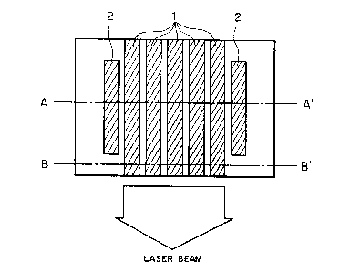
present invention, with reference to Figs. 4, 5A and 5B.
Fig. 4 is a plan view showing the ~irst
embodiment, and indicates the arrangement of stripes.
Fig. 5A is a sectional view taken along the line A-A'
of Fig. 4, that is, shows a cross section of that part
of the first embodiment where dummy stripes exist.
Fig. 5B is a sectional view taken along the line
B-B' of Fig. 4, that is, shows a cross section of that
part of the first embodiment where the dummy stripes do
not exist.
lS Referring to Figs. 5A and 5~, an n-A10 37GaO 67As
cladding layer 4, an Alo 06GaO 94As active layer 5,
a p-Alo 37GaO 63As cladding layer 6 and an n-GaAs layer
7 for narrowing a current path are successively piled on
an n-GaAs substrate 3 by the MBE (molecular beam epitaxy)
method. Then, 2 to 20 grooves each extended in the
direction of cavity length and having a width of 1 to
10 ~m for forming stripes 1 are made with a spacing of
0.5 to 5 ~m between adjacent grooves, through photo-
etching techniques so that the n-GaAs current-path
narrowing layer 7 is completely etched off and the
surface of the p-Alo 37GaO 63As cladding layer 6 is
exposed. Further, grooves for forming dummy stripes 2
are provided on both sides of a stripe region containing
- 7 -
.
,' ' - ` ~' ' ` '
,
: - .
20~ ~ ~ Qrj~j
1 the stripes 1. At this time, the width of each dummy
stripe is put in a range from 4 to 6 ~m, and each dummy
stripe is spaced apart from a confronting outermost
stripe a distance of 4 to 6 ~m. Further, the dummy
stripes 2 are not provided in that portion of the
first embodiment which has a depth of 20 to 40 ~m from
each of the front and rear facets of the present
embodiment. Next, a p-Alo 37Ga0 63As cladding layer 8
for filling up the grooves and a p-GaAs cap layer 9
are formed by the MBE method. Thereafter, a positive
electrode 10 and a negative electrode 11 are formed.
The structure thus obtained is cleaved so as to form
a laser device having a cavity length of about 300 ~m.
The above laser device was able to generate
a continuous wave having a wavelength of 830 nm, at room
temperature. In a case where three stripes were formed
in the laser device, the threshold current was equal
to 100 mA. Further, the value of threshold current
was 200 mA, 300mA and 550mA for the formation of six
stripes, ten stripes and twenty stripes, respectively.
The transverse mode of oscillation in this laser
device was a stable single mode, and phase locked
oscillation took place all over the stripe region.
[EMBODIMENT-2]
Next, explanation will be made of the second
embodiment of a semiconductor laser device according to
the present invention, with reference to Figs. 6 and 7.
Fig. 6 is a plan view showing the second embodiment,
-- 8 --
: . ~
':' , ,
~ 201~
l and indicates the arrangement of stripes. Fig. 7 is a
sectional view of the second embodiment.
Referring to Fig. 7, an n-Al0 5Ga0 50As
cladding layer 15, an Alo l4Ga0 86As active layer 16,
a p-Alo 5Ga0 5As cladding layer 17, a p-Alo 30Ga0 70As
layer 18 for improving the bottom structure of a GaAs
layer, and an n-GaAs 7 for narrowing a current path are
successively piled on an n-GaAs substrate 3 by the MOCVD
(metalorganic chemical vapor deposition) method. Then,
2 to 20 grooves each extended in the direction of cavity
length and having a width of l to 10 ~m for forming
stripes are made with a spacing of 0.5 to 5 ~m between
adjacent grooves, through photoetching techniques so
that the current-path narrowing layer 7 is completely
etched off and the surface of the p-Alo 30Ga0 70As layer 18
is exposed. Further, grooves for forming dummy stripes 2
are provided on both sides of a stripe region containing
the stripes 1. At this time, the width of each dummy
stripe is put in a range from 4 to 6 ~m, and each dummy
stripe is spaced apart from a confronting outermost
stripe a distance of 4 to 6 ~m. Next, a p-Alo 60Ga0 40As
layer 19 for filling up the grooves and a p-GaAs cap
layer 9 are formed by the MOCVD method. Thereafter, a
positive electrode 10 and a negative electrode ll are
formed. The structure thus obtained is cleaved 90 as
to form a laser device having a cavity length of about
300 ~m. Thereafter, the front facet of the laser
device is coated with a low reflecting film 14 having
_ g _
- 2 ~
1 a reflectivity RL, and that area of the rear facet which
corresponds to the stripe region, is coated with
a highly reflecting film 13 having a reflectivity RH.
Further, that area of the rear facet which corresponds to
a dummy stripe region, is coated with a reflecting film
12 having a reflectivity lower than the reflectivity
RH.
The laser diode thus obtained was able to
generate a continuous wave having a wavelength of 830 nm,
j 10 at room temperature. The value of threshold current was
100 mA, 200 mA, 300 mA and 550 mA for the formation of
three stripes, six stripes, ten stripes and twenty
stripes, respectively. Further, the transverse mode
of oscillation in the laser device was a stable single
mode, and phase locked oscillation took place all over
the stripe region.
[EMBODIMENT-3]
Explanation will be made of the third embodi-
ment of a semiconductor laser device according to the
present invention, with reference of Figs. 8 and 9.
Fig. 8 is a plan view showing the third embodiment and
indicates the arrangement of stripes. Fig. 9 is a
sectional view taken along the line A-A' of Fig. 8.
Referring to Fig. 9, an n-A10 50Ga0 50As
cladding layer 22 and an Alo 14Ga0 86As active layer
23 are successively piled on an n-GaAs substrate 3 by the
MOCVD method. Then, selective etching is carried out
for the layers 23 and 22 through photoetching techniques
:~ - 10 -
.... .
,
~ . . . ~.
;. ~ ,
: .
201~
l so that the active layer 23 is completely etched off
and the cladding layer 22 is etched to a predetermined
depch, to form stripes 20 as shown in Fig. 8 and to
form dummy stripes 21 on both sides of a stripe region.
At this time, each dummy stripe is formed so as to
have a width of 4 to 6 ~m and to be spaced apart from
a confronting outermost stripe a distance of 4 to 6 ~m.
Although it is shown in Fig. 8 that four stripes are
coupled with five stripes through Y-shaped portions,
2 to 20 stripes may be formed. Each stripe is formed
so as to have a width of l to 10 ~m. Next, a
a-Al0 50Ga0 50As cladding layer 24 for filling up etched
portions, and an n-GaAs cap layer 25 are formed by the
MOCVD method. Thereafter, zinc is diffused into a
portion which exists over the stripe region and dummy
stripe region. Reference numeral 26 in Fig. 9 designates
` a zinc diffused region. Then, a positive electrode 10
and a negative electrode 11 are formed. The structure
thus obtained is cleaved so as to form a laser device
having a cavity length of about 300 ~m.
The laser device was able to generate a
continuous wave having a wavelength of 830 nm, at room
temperature. The value of threshold current was 100 mA,
200 mA, 300 mA and 550 mA for the formation of three
stripes, six stripes, ten stripes and twenty stripes,
respectively. Further, the transverse mode of oscilla-
tion in the laser device was a stable single mode,
and phase locked oscillation took place all over the
-- 11 --
~ ~ .
:. . .. ~.
2011~
1 stripe region.
[EMBODIMENT-4]
Explanation will be made of the fourth embodi-
ment of a semiconductor laser device according to the
pxesent invention, with reference to Figs. 10 and 11.
Fig. 10 is a plan view showing the fourth embodiment,
and Fig. 11 is a sectional view taken along the line
A-A' of Fig. 10.
Referring to Fig. 11, an n-GaAs layer 29
for narrowing a current path is formed on a p-GaAs
substrate 28 by the MOCVD method. Next, 2 to 20 grooves
each having a width of 1 to 10 ~m for forming stripes
are provided through photoetching techniques so that
the current-path narrowing layer 29 is completely
etched off and the substrate 28 is etched to a
predetermined depth. Further, dummy portions 27 for
transmitting a aurrent which does not contribute
oscillation, are provided on both sides of a stripe
region. Each of the dummy portions has a width of 4 to
5 ~m, and has a length of 20 to 30 ~m in the direction
of cavity length. As shown in Fig. 10, the dummy
portions are arranged so as to be spaced apart from a
confronting outermost stripe a distance of 4 to 6 ~m
and to be spaced apart from each other a distance of
10 ~m in the direction of cavity length. Next, a
p-Alo 50GaO 50As cladding layer 30, an Alo 14GaO 86As
active layer 31, an n-A10 50GaO 50As cladding layer
32 and an n-GaAs cap layer 33 are successively formed
- 12 -
' '
` - 2011~
~ 1 by the LPE (liquid phase epitaxy) method. Thereafter,
a negative electrode 34 and a positive electrode 35 are
formed. The structure thus obtained is cleaved so as
to form a laser device having a cavity length of about
à 5 300 ~m.
' The laser device was able to generate a
continuous wave having a wavelength of 830 nm, at room
temperature. The value of threshold current was 100 mA,
200 mA, 300 mA and 550 mA for the formation of three
10 stripes, six stripes, ten stripes and twenty stripes,
r respectively. Further, the transverse mode of
oscillation in the laser device was a stable single mode,
and phase locked oscillation took place all over the
3 stripe region.
j 15 Next, explanation will be made of other embodi-
ments, in which a current can be injected into a dummy
stripe region independently of a current flowing through
a stripe region.
I [EMBODIMENT-5]
f 20 Explanation will be made of the fifth embodi-
i ment of a semiconductor laser device according to the
f~ present invention, with reference to Figs. 12 and 12A.
Fig. 12 is a plan view showing the fifth embodiment,
¦ and indicates the arrangement of stripes. ~ig. 12A is a
¦ 25 sectional view taken along the line A-A' of Fig. 12,
f that is, shows a cross section of that part of the
fifth embodiment where dummy stripes 2 exist.
Referring to Fig. 12A, an n-A10 37Ga0 63As
- 13 -
; . .
,.:. . . :: . . .
. - . . ~
. . . .
.. . . .
. ~ . .
20111~S
1 cladding layer 4, an Alo 06GaO 94As active layer 5,
a p-Alo 37GaO 63As cladding layer 6 and an n-GaAs
layer 7 for narrowing a current path are successively
piled on an n-GaAs substrate 3 by the MBE method.
Then, 2 to 20 grooves each extended in the direction of
cavity length and having a width of 1 to 10 ~m for
forming stripes 1 are made with a spacing of 0.5 to 5 ~m
between adjacent grooves, through photoetching
technlques so that the current-path narrowing layer 7
is completely etched off and the surface of the cladding
layer 6 is exposed. Further, grooves for forming dummy
stripes 2 are provided on both sides of a stripe region
containing the stripes 1. At this time, the dummy stripes
2 are formed so that each dummy stripe has a width of 4 to
6 ~m and is spaced apart from a confronting outermost
stripe a distance of 4 to 6 ~m. Further, the dummy
stripes 2 are not formed in that portion of the present
embodiment which has a depth of 20 to 40 ~m from each
of the front and rear facets of the present embodiment.
Next~ a p-Alo 37GaO 63As cladding layer 8 for filling
up the grooves and a p-GaAs cap layer 9 are formed
by the MBE method. Thereafter, a positive electrode
layer is deposited to form an electrode lOA for the
stripe region and an electrode lOB for a dummy stripe
region by the lift-off method.
As mentioned above, the electrode lOA for the
stripe region is separated from the electrode 10~ for
the dummy stripe region. Thus, a current supplied to
- 14 -
, . . . .
.
, , ~ .
.. ,, ~ ,
. , .
201~1S~
1 the dummy stripe region can be controlled independently
of a current supplied to the stripe region.
In order to separate the current flowing through
the dummy stripe region, completely from the current
flowing through the stripe region, it is necessary to
provide isolation regions 50, which can be formed by
carrying out proton implantation while using the
electrodes 10a and 10B as a mask. Thereafter, a negative
electrode 11 is formed. The structure thus obtained
is clearved so as to form a laser device having a cavity
length of about 300 ~m.
The laser device was able to generate a
continuous wave having a wavelength of 830 nm, at room
temperature. The value of threshold current was
100 mA, 200 mA, 300 mA and 550 mA for the formation of
three stripes, six stripes, ten stripes and twenty
stripes, respectively. By supplying a current to the
dummy stripe region in a period when a CW operation
was performed, the transverse mode of oscillation
became a stable single mode, that is, phase loaked
oscillation took place all over the stripe region.
Further, in a case where a pulsed operation was performed,
phase locked oscillation took place all over the stripe
region and the transverse mode of oscillation was a
stable single mode, independently of whether or not a
current was supplied to the dummy stripe region.
~EMBODIMENT-6]
Explanation will be made of the sixth embodiment
- 15 -
:: .. . . . . .
'.:' -' . ' ' '
.
. . . . . .
1 of a semiconductor laser device according to the present
invention, with reference to Figs. 13 and 13A. Fig. 13
- is a plan view showing the sixth embodiment, and
indicates the arrangement of stripes. Fig. 13A is a
5 sectional view of the present embodiment.
~? Referring to Fig. 13A, an n-A10 50Ga0 50As
cladding layer 15, an Alo 14Ga0 86As active layer 16,
a p-Alo 50Ga0 50As cladding layer 17, a p-Alo 30Ga0 70As
t layer 18 for improving the bottom structure of a GaAs
10 layer, and an n-GaAs layer 7 for narrowing a current
r path are successively piled on an n-GaAs substrate 3
¦ by the MOCVD method. Then, 2 to 20 grooves each
extended in the direction of cavity length and having
a width of 1 to 10 ~m for forming stripes 1 are made
15 with a spacing of 0.5 to 5 ~m between adjacent grooves,
through photoetching techniques so that the current-
path narrowing layer 7 is completely etched off and the
surface of the bottom-structure improving layer 18 is
exposed. Further, grooves for forming dummy stripes 2
20 are provided on the both sides of a stripe region contain-
ing the stripes 1. At this time, the dummy stripes 2
are formed so that each dummy stripe has a width of 4
to 6 ~m and is spaced apart from a confronting outermost
stripe a distance of 4 to 6 ~m. Next, a p-Alo 60Ga0 40As
25 cladding layer 19 for filling up the grooves, and a
p-GaAs cap layer 9 are formed by the MOCVD method.
Thereafter, a positive electrode layer is deposited to
form an electrode 10A for the stripe region and an
- 16 -
t.
.'.' ' ~ , `
~.~` . ~, ' ' '
201~
1 electrode lOB for a dummy stripe region by the lift-off
method.
As mentioned above, the electrode lOA for the
stripe region is separated from the electrode lOB for
the dummy stripe region. Thus, a current supplied to
the dummy stripe region can be controlled independently
of a current supplied to the stripe region.
In order to separate the current flowing
through dummy stripe region, completely from the current
flowing through the stripe region, it is necessary to
provide isolation regions 51, which can be formed by
carrying out selective etching to a depth capable of
reaching the current-path narrowing layer 7 while using
the electrodes lOA and lOB as a mask. At this time,
lS the dry etching method is used, since side etching is
scarcely generated. Thereafter, a negative electrode 11
is formed. The structure thus obtained is cleaved
so as to form a laser device having a cavity length
of about 300 ~m. Referring to Fig. 13, the front facet
of the laser device is coated with a low reflecting film
14 having a reflectivity RL, and that area of the rear
facet which corresponds to the stripe region, is coated
with a highly reflecting film 13 having a reflectivity
RH. Further, that area of the rear facet which
corresponds to the dummy stripe region, is coated with
a reflecting film 12 which is lower in reflectivity
than the highly reflecting film 13. The laser device
thus obtained was able to génerate a continuous wave
- 17 -
. : .
: .. . .
.. . . .
~ . .
, . . ... .
..~. ,
... ..
201~
1 having a wavelength of 780 nm, at room temperature.
The value of threshold current was 100 mA, 200 mA, 300 mA
and 550 mA for the formation of three stripes, six stripes,
ten stripes and twenty stripes, respectively. By
supplying a current to the dummy stripe region in a period
when a CW operation was performed, the transverse mode
of oscillation became a stable single mode. Further,
in a case where a pulsed operation was performed,
phase locked oscillation took place all over the stripe
region and the transverse mode of oscillation was a
stable single mode, independently of whether or not a
current was supplied to the dummy stripe region.
[EMBODIMENT-7]
Explanation will be made of the seventh embodi-
ment of a semiconductor laser device according to the
present invention, with reference to Figs. 14 and 14A.
Fig. 14 is a plan view showing the seventh embodiment,
and indicates the arrangement of stripes. Fig. 14A is
a sectional view taken along the line A-A' of Fig. 14.
Referring to Fig. 14A, an n-A10 50Ga0 50As
cladding layer 22, an Alo 14Ga0 86As active layer 23
and a p-Alo 50Ga0 50As cladding layer 17 are successively
piled on an n-GaAs substrate 3 by the MOCVD method.
Next, selectlve etching is carried out through photo-
etching techniques so that the active layer 23 is
completely etched out and the cladding layer 22 is
etched to a predetermined depth, to form stripes 39 as
shown in Fig. 14. Further, dummy stripes 40 for
- 18 -
.'" ~ .,' ': ,
,; : -~ .,
'.. : ~ . ' .
,, :.
201~
l transmitting a current which does not contribute to
oscillation, are provided on both sides of a stripe
region containing the stripes 39. Each of the dummy
stripes 40 has a width of 4 to 5 um, and has a length
of 20 to 30 ~m in the direction of cavity length. As
shown in Fig. 14, the dummy stripes 40 are arranged
so as to be spaced apart from a confronting outermost
stripe a distance of 4 to 6 ~m and to be spaced apart
from each other a distance of 10 ~m in the direction
of cavity length. Although it i5 shown in Fig. 14
that four stripes are coupled with five stripes
through Y-shaped portions, 2 to 20 stripes may be
formed. Each of the stripes 39 has a width of 1 to
10 ~m. Next, a slightly-doped (or undoped)
Alo 50Ga0 5As cladding layer 36 for filling up grooves,
and an n-GaAs cap layer 25 are formed by the MOCVD
method. Thereafter, zinc is diffused into a portion
which exists on the stripe region, and a portion which
exists on the dummy stripe portion, to form zinc diffused
regions 26. Then, a positive electrode layer is
deposited, to form an electrode 10A for the stripe
; region and an electrode 10B for the dummy ~tripe
region by the lift-off method. Thus, a current aan be
supplied to the dummy stripe region independently of a
current supplied to the stripe region. Thereafter,
a negative electrode ll is formed. The structure
thus obtained is cleaved so as to form a laser device
having a cavity length of about 300 ~m.
- 1 9
,~ . ' .
,:
` . '
.
201~
1 The laser device was able to generate a
continuous wave having a wavelength 780 nm, at room
temperature. The value of threshold current was 100 mA,
200 mA, 300 mA and 550 mA for the formation of three
stripes, six stripes, ten stripes and twenty stripes,
respectively. By supplying a current the dummy stripe
region in a period when a CW operation was performed,
the transverse mode of oscillation became a stable
single mode. Further, in a case where a pulsed opera-
tion was performed, phase locked oscillation took placeall over the stripe region and the transverse mode
of oscillation was a stable single mode, independently of
whether or not a current was supplied to the dummy stripe
region.
The above-mentioned technical thought that
dummy stripes are disposed on both sides of a stripe
region, is applicable to semiconductor laser devices
of all kinds including the single lobe type and the double
lobe type. Although semiconductor laser devices usually
generate a double lobed for field pattern, it is desirable
to generate a single lobed ~ar field pattern. Accordingly,
a semiconductor laser device obtained by applying the
above technical thought to a semiconduator laser device
of the single lobe type, will be the most practical
device.
Now, explanation will be made of a semi-
conductor laser device of the single lobe type proposed
by the present inventors. It is described in a Japanese
- 20 -
, . . .
2 ~
1 patent application JP-A-62-147,791 that a current is
injected into an interstripe portion sandwiched between
stripes and having a low-refractive index, to form
a single lobed far field pattern based upon oscillation
of the fundamental mode. In this case, the single
lobed far field pattern is obtained by suppressing the
mode of the N-th order.
; Fig. 15 shows relations between a ratio of
the gain at each stripe to the gain at each interstripe
portion having a low refractive index and a threshold
gain. When the gain at each stripe is decreased to
reduce the above ratio, the threshold gain of the mode of
the N-th order is abruptly increased, but the threshold
gain of the mode of the first order is gradually
increased. That is, the mode of the N-th order can be
; suppressed by reducing the above ratio. The reason for
this will be explained below. Fig. 16A shows the amplitude
distribution of electric field due to the first-order
mode, in a phased-array laser device. Fig. 16B shows the
amplitude distrubution of electric field due to N-th
order mode, and Fig. 16C shows the amplitude distribu-
tion of electric field due to the (N+)th order mode.
In Figs. 15 and 16A to 16C, reference numeral 41
designates stripes, and 42 interstripe portions. In the
~ 25 first-order mode, adjacent stripes have the same
;l oscillation phase, and thus the amplitude of electric
field at a portion sandwiched between the stripes
¦~ ~namely, interstripe portion) is not equal to zero.
,
.
. '
2 0 1 ~
1 Accordingly, when the ratio of the gain at the stripe to
the gain at the interstripe portion is reduced, the
threshold gain is increased only a little. While, in
the N-th order mode, adjacent stripes are opposite in
oscillation phase to each other, and thus the amplitude
of electric field at the interstripe portion becomes
equal to zero. That is, the electric field intensity
at the interstripe portion is far weaker than the electric
field intensity at the stripe. Accordingly, when the
ratio of the gain at the stripe to the gain at the
interstripe portion is reduced, the threshold gain is
greatly increased. In the (N+)th order mode, oscillation
of a higher mode is generated in each stripe. Thus,
the amplitude of electric field becomes equal to zero
in each stripe, and the amplitude of electric field at
the interstripe portion is not equal to zero. That is,
the electric field intensity at the interstripe portion
; is stronger than that in the first-order mode. Accord-
ingly, when the ratio of the gain at the stripe to the
gain at the interstripe portion is reduced, an increase
in threshold gain will be smaller than that in the
first-order mode. That is, the mode of the ~N+l)th order
is generated.
Figs. 17a, 17B and 17C show the far field
2S patterns of the first-order mode, the N-th order mode
and the (N~l)th order mode, respectively. In the first-
order mode, a single lobed pattern is formed as shown
in Fig. 17a. While, in the N-th order mode and (N+l)th
.- . -'': ` :
:: , .
:
2 ~
l order mode, a double lobed pattern is formed which is
undesirable from the practical point of view.
It is well known that the modes of the (N+l)th
order and a higher order than the (N+l)th order can be
suppressed in the semiconductor laser device of this
kind by ~arrowing the width of each stripe. Further,
it has been confirmed by the present inventors that
in a case where a current injected into a stripe is
decreased to reduce the gain at the stripe as mentioned
above, the modes of the (N+l)th order and a higher order
than the (N+l)th order can be suppressed by making the
width of the stripe less than 3 ~m.
That is, in a case where a semiconductor device
includes a plurality of stripes each having a width
less than 3 ~m and a current injected into each stripe
is reduced (or a current injected into each interstripe
portion is increased), the mode of the N-th order is
cut off on the basis of the threshold gain characteristic
thereof shown in Fig. 15, and the modes of the (N+l)th
order and a higher order than the ~N+l)th order are
cut off on the basis of the narrowing of each stripe.
Thus, modes of the N-th order and a higher order than
the N-th order are cut off, and a single lobed for
field pattern is formed.
Now, explanation will be three examples of a
semiconductor laser device of the single lobe type
based upon the above technical thought, and the
eighth to tenth embodiments of a semiconductor laser
- 23 -
: . - ?
,
--" 201~
; l device according to the present invention which embodi-
ments are obtained by adding a dummy stripe region
to the above examples.
[ EMBODIMENT- 8 ]
Explanation will be made of the first example
of a semiconductor laser device of the single lobe
type which example is used as the mother structure of
the eighth embodiment, with reference to Figs. 18A to
18C .
Fig. 18A is a sectional view showing the
first example. Referring to Fig. 18A, an n-A10 37Ga0 63As
cladding layer 4, an Alo 06Ga0 g4As active layer 5,
a p-Alo 37Ga0 63As cladding layer 6 and an n-A10 37Ga0 63As
layer 45 for narrowing a current path are successively
piled on an n-GaAs substrate 3 by the MOCVD method.
Then, 3 to 21 grooves each extended in the direction
of cavity length and having a width of 0.5 to 5 ~m for
forming interstripe portons 62 are provided through
photoetching techniques so that the current-path
narrowing layer 45 is completely etched off and the
surface of the p-Alo 37Gao 63As cladding layer 6 is
exposed. Thus, a stripe 61 having a width of 1 to
2.9 ~m is formed between adjacent grooves. Nqxt, a
p-Alo 50Ga0 50As cladding layer 24 for filling up the
grooves, and an n-GaAs cap layer 25 are formed by the
MOCVD method. Thereafter, zinc is diffused into a
region which exists over a stripe region, to form
a zinc diffused region 26 including the cap layer 25
- 24 -
,..~
., ~
... ., , . - :
-` 2 ~
l and a surface portion of the groove filling layer 24.
Then, a positive electrode 10 and a negative electrode 11
are formed. The structure thus obtained is cleaved so as
to form a laser having a cavity length of about 300 ~m.
Figs. 18B and 18C show the effective-index-of-refraction
distribution and gain distribution in this laser device.
A portion where the current-path narrowing layer 45 is
left unetched, has a large effective index of
refraction. Further, a current flows only in an
interstripe portion, and a gain is obtained only
at the interstripe portion.
The laser device was able to generte a continuous
wave having a wavelengh of 830 nm, at room temperature.
The value of threshold current was 100 mA, 200 mA and
300 mA for the formation of three stripes, six stripes and
ten stripes, respsctively. Further, in the laser device,
oscillation took place stably in the first-ordex mode,
and a single lobed for field pattern was obtalned.
When a dummy stripe region is provided on
both sides of the stripe region of the above semi-
conductor laser device of the single lobe type, and
means for supplying a current which does not contribute
to oscillation, to the dummy stripe region is provided,
- the eighth embodiment of an inventive semiconductor
laser device is obtained.
~EMBODIMENT-9]
Explanation will be made of the second example
of a semiconductor laser device of the single lobe type
- 25 -
.
: ~' -'.' ' '` ' ' '' ,' ' '' ~
., . ~ ,
: . , .
-- 2 0 1 ~
1 which example is used as the mother structure of the
ninth embodiment of a semiconductor laser device
accoxding to the present invention, with reference to
Figs. l9A to l9C.
Fig. l9A is a sectional view showing the second
example. Referring to Fig. l9A, an n-A10 37Ga0 63As
cladding layer 4, an Alo 06~a0 94As active layer
5, a p-Alo 37Ga0 63As cladding layer 6, a p-GaAs absorp-
tion layer 67 and an n-GaAs layer 7 for narrowing a
current path are successively piled on an n-GaAs
substrate 3 by the MOCVD method. Then, a groove 63
for defining a stripe region is provided through
photoetching techniques so that the current-path narrow-
ing layer 7 is completely etched off and the surface of
the absorption layer 67 is exposed. Thereafter, 3 to
21 grooves each extended in the direction of cavity
length and having a width of 0.5 to 5 ~m for forming
interstripe portions 62 are provided through photoetching
techniques so as to reach the surface of the
p-Alo 37Gao 67As cladding layer 6. At this time, a
portion sandwiched between adjaaent grooves and having
a width of 1 to 2.9 ~m is formed as a stripe 61. Next,
a p-Alo 37Gao 63As cladding layer 8 for filling up the
grooves, and a p-GaAs cap layer 9 are formed by the
MOCVD method. Then, a po~itive electrode 10 and a
negative electrode li are formed. The structure thus
obtained is cleaved so as to form a laser device having
a cavity length of about 300 ~m. Figs. l9B and l9C
- 26 -
.
~ . :
. . . ,i
;`' ~ , ' .
201~S~
1 show the effective-index-of-refraction distribution and
gain distribution in the above laser device, respectively.
A portion where the absorption layer 67 is left unetched,
has a large effective index of refraction, and forms a
stripe 61. The current-path narrowing layer 7 is
present on both sides of the stripe region 63. Hence,
a current flows only in the stripe region 63. At the
stripe 61, the absorption layer 63 is left unetched.
Accordingly, the loss due to absorption is generated at
the stripe. Thus, a gain is obtained only at the
interstripe portion.
The above laser device was able to generate a
continuous wave having a wavelength of 830 nm, at room
temperature. The value of threshold current was 100 mA,
lS 200 mA and 300 mA for the formation of three stripes,
six stripes and ten stripes, respectively. Further,
in the laser device, oscillation took place stably in
¦ the first-order mode, and a single lobed far field
pattern was obtained.
Ey providing a dummy 8tripe region on both
sidec of the stripe region 63 of the above laser device,
,~ we can obtain the ninth embodiment of a semiconductor
laser device according to the present invention.
EMBODIMENT-10~
Next, explanation will be made of the third
example of a semiconductor laser device of the single
lobe type which example is used as the mother structure
of the tenth embodiment of a semiconductor laser device
- 27 -
` : . . '
; : ,,
: . .
.
2 0 ~ $
l according to the present invention, with reference to
Figs. 20A to 20C.
Fig. 20A is a sectional view showing the third
example. Referring to Fig. 20A, an n-A10 37Ga0 63As
cladding layer 4, an Alo 06Ga0 94As active layer 5,
a p-Alo 37Ga0 63As cladding layer 6 and an
n-Al0 37Ga0 67As layer 45 for narrowing a current path
are successively piled on an n-GaAs substrate 3 by the
MOCVD method. Then, 3 to 21 grooves each extended
in the direction of cavity length and having a width
of 0.5 to 5 ~m for forming interstripe portions 62 are
provided through photoetching techniques so that the
current-path narrowing layer 45 is completely etched
off and the surface of the p-Alo.37Ga0.63As g
layer 6 is exposed. At this time, a portion which is
sandwiched between adjacent grooves and ha~ a width
of l to 2.9 ~m, is left as a stripe 61. Next, a
p-Alo 50Ga0 50As cladding layer 24 for filling up the
grooves, and a p-GaAs cap layer 9 are formed by the
MOCVD method. Then, a portion other than a stripe region
63 is etched through photoetching techniques so that the
p l0,37Ga0,67As cladding layer 6 is
exposed. At this time, an SiO2 film is used as an
etching mask. Thereafter, the selective growth of an
n-GaAs layer 7 for narrowing a current path is carried
out while u9ing the SiO2 film as a mask. After the SiO2
film has been removed, a positive electrode 10 and a
negative electrode 11 are formed. The structure thus
- 28 -
.
:
,
2 ~
1 obtained is cleaved so as to form a laser device having
a cavity length of about 300 ~m. Figs. 20B and 20C
show the effective-index-of-refraction distribution and
gain distribution in this laser device. A portion where
the current-path narrowing layer 45 is left unetched,
has a large effective index of refraction, and forms a
stripe 61. Since the current-path narrowing layer
45 is left in the stripe 61, no current flows in the
stripe. Further, no current flows on the outside of the
stripe region 63, since the current-path narrowing
layer 7 is formed on the outside of the stripe region 63.
Thus, a current flows only in the interstripe portions
62, and a gain is obtained only at the interstripe
portions 62.
The above laser device was able to generate a
continuous wave having a wavelength of 830 nm, at room
temperature. The value of threshold current was 100 mA,
200 mA and 300 mA for the formation of three stripes,
six stripes and ten stripes, respectively. Further,
in the laser device, oscillation took place stably in the
j first-order mode, and a single lobed far filed pattern was
obtained.
By providing a dummy stripe region on both side
edges of the stripe region 63 of the above laser device,
we can obtain the tenth embodiment of a semiconductor
laser device according to the present invention.
t In the above-mentioned embodiments, a laser beam
having a wavelength of 780 or 830 nm was emitted. In
- 29 -
. , '` `
,,, ' , '
,, .
. .
, , .
201~1$5
1 AlGaAs laser devices according to the present invention,
however, the wavelength of the emitted laser beam is not
limited to the above values, but a continuous wave
having a wavelength of 680 to 890 nm can be generated
at room temperature. In the embodiments, only one
AlGaAs layer is used as an active layer. Alternatively,
an active layer of the MQW (multi-quantum well) structure
formed of an AlGaAs superlattice may be used. Further,
in the embodiments, a three-layered waveguide is used
as a fundamental element. However, a semiconductor layer
device according to the present invention may have an
LOC (large optical cavity) structure, in which an
optical guide layer adjacent to an active layer is
formed only on one side of the active layer, or a
GRIN-SCH (graded-index-separate-confinement-
heterostructure) ætructure, in which an optical guide
layer adjacent to an active layer is formed on both
sides of the active layer.
Further, semiconductor laser devices each made
up of semiconductor layers opposite in conductive type
to semiconductor layers included in one of the embodi-
ments, can produce the same effect as obtained by the
embodiments.
Although AlGaAs layers are used in each of
: 25 the embodiments, AlGaP layers, AsAlInP layers, AsAlGaInP
layers, or AlGaInAs layers may be used in place of the
AlGaAs layers.
As has been explained in the foregoing,
- 30 -
.~ . .
'
.
-
20111 ~
1 according to the present invention, a portion for
transmitting a current which does not contribute to
oscillation, is provided on both sides of a stripe region,
to make uniform the temperature distribution in the stripe
region. Thus, in a phased array semiconductor laser
device according to the present invention, phase coupled
oscillation is generated all over the stripe region,
even when a CW operation is performed. That is,
oscillation of a single transverse mode is obtained,
and a laser beam is emitted which is excellent in
coherency.
- 31 -
- ;,' - ~ :
' :
: .. . .
:: ~
. ~ -
: ~-