Note : Les descriptions sont présentées dans la langue officielle dans laquelle elles ont été soumises.
20112~
BACKGROllND OF THE INVENTION
This invention finds use in digitfal radio communications systems where the
receive signal demodulator oscillator is phase synchronized with the transmitteroscillator. It is particularly well suited to obtaining fast synchronization or locking
and subsequently maintaining lock in the presence of burst noise and when the
received power level is very low, that is where the receive signal power level is very
near to a minimum Carrier to Noise (C/N) ratio that is needed for communicationsto occur. Such conditions occur in communications systems using satellite
communications technology; in distant radio communications where transmitter power
is either expensive to provUe, such as in a remote location, or is limited by spectrum
Iicensing or regulation ~o a maximum power level; and in fibre optic communication
where maximum distances between repeater sites is needed (e.g. undersea cables).
A problem in modern digital communications is knowing when the
demodulator is in and out of lock with the transmitter. Knowing the lock condition
enables the designer to implement bandwidth switching in the demodulator to helpincorporate fast locking (wide bandwidth) and secure locking (narrow bandwidth).Present lock detect circuits are incorporated at tfhe I~ demodulator, and have problems
of cost, implementation, and reliability in low C/N operation.
When the communications signal is encoded with forward error correction, it
is possible to implement a lock detect circuit based upon the quality of the received
data. This method of obtaining bandwidth switching provldes several benefits:
- high reliability based on the received data;
- a digital implementation which is simple and cost effective;
- separate digitally setable wide-to-narrow and narrow-to-wide
thresholds;
- bandwidth switching which is cycle slip resistant.
., ~
r. : : .
~, . .
': : .
'
~11264
SUMMARY OF THE INVENTION
;
The present invention relates generally to a novel apparatus and method for
switching a phase-locked loop demodulator feedback loop bandwidth from wide-bandto narrow-band based on the bit error rate of the received signal.
In one of its aspects, the invention provides a receiver for tracking a carrier
suppressed phase-shifted input signal comprises a phase-locked loop circuit for
receiving the input signal and having a variable frequency oscillator responsive to a
control signal for oscillating at a frequency corresponding to an intermediate
frequency and a frequency difference detector for producing an output signal
indicative of the frequency difference between the frequency of the input signal and
the intermediate frequency, a feedback loop network having a narrow-band path and
a wide-band path and being responshe to the detector output signal for producing the
control signal and applying the control signal to the oscillator through one of the paths
whereby to change the intermediate frequency of the oscillator in response to the
control signal, a quality detector responsive to the detector output signal for
producing a signal corresponding to the bit error rate of the input signal; and selection
means responsive to the bit error rate signal for causing the control signal to pass
through the narrow-band path when the bit error rate signal is below a predetermined
threshold and through the wide-band path when the bit error rate signal exceeds the
predetermined threshold.
In another of its aspects, the present invention provides a method of
communicating digitally encoded inforrnation by a carrier suppressed eleckomagnetic
transmission including the steps of:
a. encoding the information to be kansmitted with redundant bits in
accordance with a selected algorithm;
b. producing a frequency-variable recovered carrier signal from the
received transmission using a closed-loop Costas loop demodulator
having at least two feed-back loop paths of different bandwidth;
,. :
,, ~.
: . . ...
.... . . ...
3201~26~
c. multiplying the received transmission with the recovered carrier signal
to recover the modulating signal;
d. processing the recovered modulating signal to determine the digital
information encoded therein including the redundant bits;
e. decoding the digital inforrnation by computing the redundant bit
algorithm to produce a bit error signal;
f. counting the bit error signals; and
g. selecting one of the feed-back loop paths at predetermined count
thresholds within a selected time interval.
BRIEF DESCRIPIION OF THE DRAWINGS
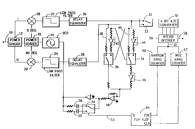
~ ggure 1 shows in functional block diagram form a receiver incorporating the
features of the invention.
DETAILED DESCRImON
The demodulator of the receiver system decodes information modulated onto
a carrier signal using Quadrature Phase Shift Keying (QPSK). A known demodulatorfor demodulating such a signal is referred to as a Costas loop. The Costas loop
implementation of a QPSK demodulator in accordance with the present invention isshown in the attached ~lgure 1. As shown in this figure, the demodulator input
intermediate frequency (IF) signal at point 10 is power divided into a phase (O) I
signal and quadratu~e (90) Q signal by power divider 12. A voltage controlled
crystal oscillator (VCXO) 14 is used as a VCO in the carrier recovery loop. For
example, a 10.7 MHz VCXO can be used to match the IF frequency used in the
receiver Rl~/IP stage. The VCXO output is power divided by power divider lC intoa phase (O - I) and quadrature (90 - Q) signal in the same fashion as the input IF
signal was. The 10.7 MHz O and 90 signals are multiplied by the 10.7 MHz inputintermediate frequency IF signals by multipliers 18 and 20. The multiplier outputs
are low pass filtered using, for example, a 40 KHz wide low-pass filters 22 and 24~
The resultant filtered signals are group delay-equalized by delay equalizers 26 and 28
': .. . . ,.
.. ~ -
;- ,
-^ 20112~
- 4 -
to remove any phase-delay distortion which is introduced into the 0-40 KHz frequency
range by the low-pass filters 22 and 24.
.
A four bit Analog to Digital (A/D) converter 30 is used to obtain the four bit
A/D decoding of the I and Q signals. The decoding is 1 bit for sign and 3 bits for
magnitude. In the illustrated embodiment, a single A/D converter is multiplexed
between the I and Q channel by analog switch 32 to allow one A/D converter to beused for both channels. The switching of the A/D converter from the I channel tothe Q channel is controlled by a clocking derived from the recovered carrier which
is counted down to a switching pulse at control point 33. This switching pulse allows
both the I and Q sample to be taken by the A/D converter for each data element that
is received. It will be understood that it is possible to implement the circuit using 2
A/D converters, 1 for the I channel and another for the Q channel.
Now looking at the feedback loop of the decoder. The I and Q channel analog
signals are selected in-phase or 180 phase by the sign bit of the other channel. The
in-phase and 180 phase switching is done by means of the cross-sampling of the I
and Q channels. The so sampled signal is used to control analog switch 34 or 36
(one being provided for each channel) which switch takes the I or Q channel signal
directly on paths 38 or 40 or through an inverter 42 or 44. The two thusly-switched
outputs are subtracted (by passing the switched I channel analog signal through
inverter 46 and summing the two channels using Op-Amp 48 and low-pass filtered
by means of Op-amp feedback path S0 or S2 to obtain the feedback control voltagesignal for the carrier VCXO. The selection of a wide-band feedback path S0 at 0.9%
of the symbol rate, or coded data rate, or a narrow-band feedback path S2 at 0.2%
of the symbol rate is made by analog switch S4 which is operated in the manner
described below. It is the selection of one or the other of these feedback paths which
determines the closed-loop demodulator bandwidth as being either narrower or wider.
As the loop signal to noise (SNR) ratio improves with a narrowing of the demodulator
feed-back loop bandwidth, a narrower demodulator bandwidth allows a locked signal
to be decoded with better reliability. These processing circuits in the Costas loop
remove the modulating data and generate a frequency control voltage thus resulting
,;, - ,
; -
,, ,
.',, : ,
' ' - ' ' . . .: ~ ,
, .
.,~ , . ,
20~126~
s
in automatic frequency control (AFC) action of the VCXO 14. The locked (narrow-
band mode) feedback-loop filter bandwidth is designed to be about 0.2 percent of the
symbol rate of the transmission. The symbol rate would be 2 or 3 times the data
transmission rate depending on whether rate 1/2 or rate 1/3 convolution encoding is
performed on the transmitted data. An example data transmission rate would be 56Kilo Bits per second (KBps). The loop is initia11y in a wide-band mode which is
preferably approximately 0.9 percent of the symbol rate, to enable the receiver to
quickly settle into a locked state. Once a locked state has been achieved, the analog
switch S4 is set by control line S3 to the narrow-band mode to make the receivermore noise-immune. The bandwidth of these filters determines the receiver systemclose-loop noise bandwidth and the switching of this bandwidth from wide (out-of-
lock) to narrow (in-lock) will be explained later.
The Viterbi Decoder S6 is an off-the-shelf single LSI chip, as for example the
ST-2010 VITERBI DECODER manufactured by Stanford Telecommunications Inc.
of Santa Clara, California, which takes in the 4 bit parallel I and Q samples provided
by the A/D converter 30 and produces a data stream out. The 4 bit I and Q channel
data is input into the decoder chip. The decoder S6 may lock into one of the four
QPSK phases, namely: 0, 90, 180, or 270. Two of these phases provide the
data sought. The first phase, at 0, is the desired phase to lock into. The second
desirable phase, at 180, just inverts the data and the differential encoding and
decoding of the data takes care of this arnbiguity. If the loop locks into one of the
other two phases (90 or 270), the I and Q inputs have to be swapped. This
swapping is done if the data quality output shows a poor data quality for a timeexceeding a preset interval.
The indicated decoder chip requires a clock signal which is 80-140 times the
symbol rate. As an illustration, a 7.168 MHz VCXO (not shown) at 128 times the
symbol rate is used to generate this clock signal for the decoder chip. This VCXO
is locked to the data clock using a bit synchronizer circuit (not shown). Differential
decoding of the data is carried out inside the chip. A V.35 descrambler (not shown)
could be used at the decoder output S8 to descramble the data, assuming it was
B
.. .
~,
: .
,. . . .
,.. . . .
r ~ ~ ~
2 ~
- 6 -
scrambled at transmission by a V.35 scrambler, which is the preferred way of
scrambling the transmitted signal. The 56 Kbps descrarnbled data output from theV.3S decoder may then be fed into a mux (not shown).
When the receiver demodulator is first powered up, it must become phase
synchronized with the transmitter. To become synchronized quickly, it is desirable
to have the receiver VCXO control loop have a wide bandwidth. Once synchronized,it is desirable to have the receiver VCXO control loop have a narrow bandwidth
making the receiver less likely to get out of synchronization with the transmitter
owing to burst noise or cycle slip (ie moving 90 into a different quadrature, that is
from 0 to 90 etc.).
The convolution encoding used in the present system provides extra coding
bits which are decoded out during the Viterbi decoding process by the decoder 56.
The extra coding bits are checked using a decoding algorithm during the Viterbi
decoding process to check on receive data integdty. The use of the decoding
algodthm allows the Viterbi decoder to determine if any bit errors have occurred in
the inbound data. As errors occur they are signalled on data quality line 61 which
is fed into counters C0 and C2. When an error rate below a threshold error rate is
achieved over a fixed pedod of time, it is known that the demodulator is in lock. It
is desirable at this time to reduce the locking bandwidth of the demodulator to
maintain the locked state. Once the demodulator i9 in narrow-band mode, the phase
locked loop of the demodulator is not capable of rapid movement in the frequency
domain.
In the preferred embodiment of the invention, the wide-band narrow-band state
of the phase locked loop is conttolled by flip flop 64 the output of which is used to
activate analogue switch S4 through use of control line S3.
When the decoder is in wide-band mode, for example when the demodulator
is just turned on or is attempting to resynchronize, narrow-band counter 60 counts the
errors coming from the Viterbi Decoder S6 to determine if they are smaller than a
L ii
'~ , , ' ' ' .
. , , ' , .
:. . ..
.: - - ~ .
'~ - .
2a~ 6~
- 7 -
specified count in a given time-frame. For example at a data rate of 56 kilobits per
second, a threshold of less than 32 errors in a block of 4096 bits. If such a threshold
is achieved, then narrow band counter 60 activates the PR~3set line of flip flop 64
causing it to place a voltage representing logical "1" on output "Q" which activates
analogue switch 54 to place the narrow-band feedback path 52 into the feedback loop
of the decoder. If the threshold is reached before the end of a block of 4096 bits (ie.
more than 32 errors were counted), the narrow-band counter simply resets to zero and
the counting resumes for the ne~t block of 4096 bits.
When the decoder is in narrow-band mode, wide-band counter 62 counts the
errors coming from the Viterbi Decoder S6 to determine if they are greater than a
specified count in a given time-frame. For example at a data rate of S6 kilobits per
second, a threshold of more than 2048 errors in a block of 131,072 bits. If such a
threshold is achieved, then wide-band counter 62 activates the CLeaR line of flip flop
64 causing it to place a voltage representing logical "0" on output "Q" which activates
analogue switch S4 to place the wide-band feedback path 50 into the feedback loop
of the decoder. If the threshold is not reached at the end of the block of 131,072 bits
(ie. less than 2048 errors were counted), the wide-band counter simply resets to zero
and the counting resumes for the next block of 131,072 bits.
As may be appreciated, the narrow-band and wide-band thresholds may be
varied to suit the needs of the communications system employing this method of loop-
bandwidth contrd. As the counters 60 and 62 are any suitable counter, for example
74HC4040 12 bit counters produced by Texas Instruments, any desired error rate may
be selected by choosing the desired count lead out of the counter chip. If more than
a 12 bit count is required (le. more than 2048), higher values may be obtained by
staging 2 or more counters together using configurations well known to one skilled
in thc art.
When in locked state, the demodulator control circuit responds to errors from
the decoder by treating the errors as simply a burst of errors caused by a noise burst.
The demodulator remains in narrow-band mode. Should the error rate persist, the
!
.. . .
~; .
2 ~
Viterbi decoder chip S8 responds by treating the errors as a cycle-slip and the I and
Q channel data into the decod~r are swapped and the demodulator remains in narrow-
band mode. Should the error rate persist past a second setable threshold, the
demodulator loop control circuit wide-band counter 62 is triggered. This results in
the loop-control circuit switching the loop feedba~k filter into wide-band mode by
causing flip flop 64 to be set. This in turn causes analog switch 54 to connect wide-
band path S2 to be used as the feed back path in place of nalrow-band path 50. Thus
the carrier recovery loop responds by treating the errors as caused by loss of
synchronization with the transmitter and the demodulator is switched into wide-band
mode to more quickly re-establish synchronization with the transmitter.
From the foregoing description, it will be apparent that there has been
provided an improved phase lock loop receiver having a switchable feed back loopfilter controlled by the error rate of the received signal. Naturally, the system has
been described in simplified form for clarity of description and exposition of the
invention. Additions, variations and modifications of the system described herein will
occur to those skilled in the art and are intended to be within the scope of theinvention as recited in the claims appended hereto.
~ .