Note : Les descriptions sont présentées dans la langue officielle dans laquelle elles ont été soumises.
2~1 2163
-- 1 --
The present invention relates to a digital signal
decoding circuit used for discriminating a code of a
received digital signal in, e.g., a digital radio
co~munication system.
In a digital radio communication system, a
transmission station converts codes of a digital
signal, i.e., ~1" and "o~ into a change in frequency or
voltage value, and transmits the signal. A reception
station receives and demodulates a signal sent from the
transmisslon side, and compares the received digital
signal with a signal level of a reference signal to
discriminate the codes ("1" and "0").
A conventional decoding circuit of this type has
the following problems. More specifically, a reference
slgnal level is fixed in advance to a predetermined
value. For example, assume that a varlatlon ln
modulation/demodulatlon frequency or a variation in
voltage value occurs ln a transmlsslon or receptlon
station, and a DC level of a received digital signal
is changed. In thls case, accurate code discrimination
cannot be performed, and as a result, a decoded output
includes an error.
The presQnt invention provides a digital signal decoding
circuit which can accurately decode a received digital signal
without being influenced by a change in DC level of the
received digital signal.
~ '
';, ' ' : . .
~ - .
. ~ ' .
",
2~12163
- 2 -
The present invention also provides a digital ~ignal
decoding circuit which can eliminate an influence of a change
in signal value of a received digital signal even if the
ignal value of the received digital signal is temporarily
and abruptly changed due to noise components.
Further, the present invention provides a digital signal
decoding circuit which can accurately decode a received
digital signal without being influenced by a change in
amplitude of the received digital signal.
More particularly, according to an
aspect of the present invention, the dlgital slgnal
decoding circult comprises a detector, a reference
signal generator, and a dlscrlmlnator. The detector
detects a central value of an amplltude of each bit
of interest of a received digital signal. The reference
signal generator generates a reference signal having a
signal value according to the central value detected
by the detector. The discriminator compares the signal
value of the received signal value wlth that of the
reference signal generated by the reference signal
generator in each bit of interest, thereby outputting
a decoded binary signal.
2s As a result, according to the present invention,
a signal level of a reference signal is always set to be
a central value of a received digital signal. For this
- ', '
:: ~
'. '- . .
2~121~
-- 3
reason, even if a variatlon in modulation/demodulation
frequency or in voltage value occurs ln a transmlssion
or reception station and a DC level of a recelved
digital signal is changed accordingly, the signal level
of the reference signal can be changed to follow the
change in DC level. Therefore, the codes ~ and "0~
of the received ~igltal signal can always be discrimi-
nated based on an optimal reference signal level.
Thus, high-quality decoding free from errors can be
executed.
As the detector for detecting a central value
of an amplitude, a circult for detecting maximum and
minimum values of an amplitude of each blt of interest
of a received digital slgnal, and obtalnlng the central
value of the amplltude of the recelved dlgital slgnal
on the basis of the detected maxlmum and mlnlmum values
is used. ~urthermore, as another detector for obtalnlng
a central value of an amplltude, a clrcult for detectlng
one of maximum and minimum values of an amplltude of
each bit of lnterest of a recelved digital signal,
~ and adding/subtracting a predetermined offset value
¦ to~from the detected slgnal value to obtain the central
value of the amplltude of the recelved dlgital slgnal is
used. By using these clrcults, the cen~ral value of the
amplltude of the received digital signal can be easily
1 detected.
I Also, according to
~' X
, . - ~
2~2163
-- 4
another aspect of the present invention, the digital
signal decoding circuit further comprlses an average
value detector. The average value detector obtains an
average value of central values detected for a plurality
of bits of interest. The reference signal generator
generates a reference signal having a signal value
according to the average value.
According to the present inventlon, the average
value detector obtalns an average value of central
values of amplltudes obtained for a plurality of
prevlous blts of interest, and a signal value of a
reference signal is set on the basls of this average
value. For this reason, even lf an amplitude value of
a received digital slgnal ls temporarlly and abruptly
changed due to nolse components, a reference signal
level can be prevented from being set according to the
central value of the amplitude which suffers from the
lnfluence of the change. Therefore, a stable reference
slgnal can always be generated, and accurate code
dlscrlmlnatlon can be executed whlle ellmlnatlng an
lnfluence of nolse components.
Further, according to still another aspect of the
present invention, a signal value of a received digital
s~gnal is detected on the basis of a reference signal
2s
level, and codes of the received digital signal are
di~criminated based on the detected signal value and
. j~, . .
~,~
. . - . ' . .
.
2012163
a signal value detected for a previous blt of lnterest.
Parameter data is generated according to the signal
value of the recelved digltal signal, and data asso-
ciated with the DC level of the received digital
signal is detected on the basis of the parameter data
and the signal value of the recelved digltal slgnal. A
reference slgnal level is generated on the basis of an
average value of data associated wlth the DC level.
More speciflcally, accordlng to the present invention,
code dlscriminatlon of the present blt of lnterest ls
performed with reference to a signal value detected for
a previous bit of interest (e.g., a signal value of an
immediately preceding bit of interest). In accordance
with the slgnal value of the received digital signal,
the DC level ~e.g., the central value of an amplltude)
of the recelved dlgltal signal ls obtalned, and a
reference slgnal level ls set based on the DC level.
Therefore, accordlng to the stlll another aspect
of the present inventlon, even lf an amplltude value
of a recelved digltal signal is changed accordlng to a
code pattern, a reference signal level is kept stable
; wlthout being lnfluenced by the change ln amplltude.
~-~ For this reason, a code discrimlnation error caused by
~ the change ln amplltude of the received dlgltal slgnal
;~ 25 can be prevented.
Thls lnventlon can be more fully understood from
the following detalled description when taken in
. :.
.
201~163
-- 6 --
con~unction with the accompanylng drawings, in which:
Fig. 1 is a block dlagram showing an arrangement of
a digital signal decoding clrcuit according to the first
embodiment of the present invention;
Figs. 2 to 4 are signal waveform charts for
explaining an operation of the decoding circuit shown ln
Fig. l;
Fig. 5 is a block diagram for explaining a
modification of the decoding circuit shown in Fig. l;
Fig. 6 is a signal waveform chart for explaining an
operation of the circuit shown in Fig. 5;
Fig. 7 is a block diagram showing an arrangement of
a digital signal decoding circuit according to the
second embodiment of the present invention;
Fig~ 8 is a circuit diagram partially showing the
decodlng circuit shown in Fig. 7;
Flgs. 9 and 10 are signal waveform charts for
explaining an operatlon of the decodlng clrcuit shown in
Flg. 7;
Flg. 11 i8 a block diagram showlng an arrangement
of a dlgltal slgnal decoding clrcuit accordlng to the
thlrd embodlment of the present lnventlon;
Flgs. 12 and 13 are flow charts showing control
sequences of a CPU of the decodlng clxcuit shown ln
~; 25 Flg. 11;
Flg. 14 ls a block diagram showing an arrangement
of a dlgltal slgnal decoding circuit according to the
~ .. .. . .
,
.
. .
, ~ ~ ': ,
-` 2012163
-- 7
fourth embodiment of the present inventlon;
Fig. 15 ls a circuit diagram partially showing the
arrangement of the decoding circuit shown in Fig. 14;
Figs. 16 and 17 are signal waveform charts for
explaining an operation of the decoding circult shown ln
Fig. 14;
Fig. 18 is a block diagram showing an arran~ement
of a digltal slgnal decoding clrcult accordlng to the
flfth embodlment of the present lnventlon; and
Figs. 19 and 20 are signal waveform charts for
explainlng an operatlon of the decodlng clrcult shown ln
Flg. 18.
~Flrst Embodlment)
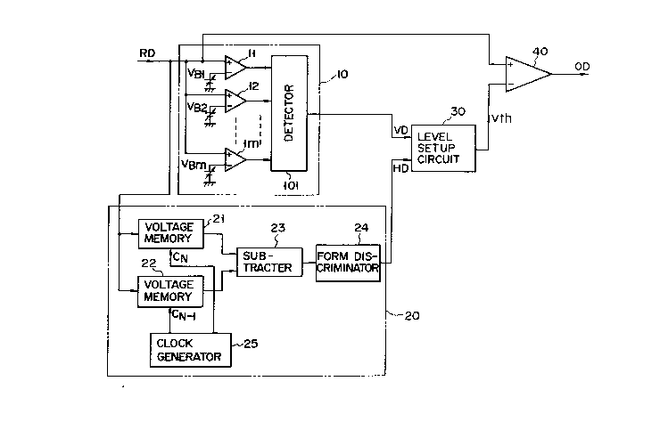
Fig. 1 is a block diagram showlng an arrangement of
a digital signal decoding circuit according to the first
embodiment of the present lnventlon.
~he decodlng circult comprises a first detectlon
circuit 10, a second detection clrcuit 20, a level
setup circult 30, and a comparison circult 40.
The flrst detectlon clrcult 10 detects a slgnal
value of a recelved dlgltal slgnal RD, and comprises a
plurality of comparators 11 to lm, and a detector 101
for detecting a voltage range. The plurality of com-
parators 11 to lm compare the recelved dlgital RD with
predetermined reference voltages Vgl to Vgm. The com-
parators output detectlon signals each of whlch goes to
"H" level when the slgnal value of the recelved digital
-: ' '' ~ . .
`` 2012163
signal RD is equal to or larger than a corresponding one
of the reference voltages vBl to vBm, and otherwise,
goes to ~L" level. The reference voltages vBl to VBm
are set as follows. More specifically, the voltage vBl
is set to be a ground level. The voltage vB2 is set to
be a value obtained by adding a given voltage value to
the voltage VBl, and the voltage VB3 is set to be a
value obtained by adding the given voltage value to the
voltage VB2. Similarly, the voltages VB4 to VBm are set
to be values obtalned by adding the given voltage value
to the voltages VB3 to VBm_l, respectivel~. The detector
101 comprises, e.gl, an encoder. The detector 101 enco-
des the detection slgnals output from the plurallty of
comparators 11 to lm and outputs, by thls encoding,
slgnal value detectlon data VD representlng a voltage
: range to whlch the slgnal value of the presently
recelved dlgltal slgnal RD belongs. The slgnal value
I detectlon data VD is supplled to the level setup clrcult
30.
The second detectlon clrcuit 20 is used to detect a
change form of the slgnal value of the recelved dlgltal
slgnal RD, and lncludes two voltage memorles 21 and 22,
and a clock generator 25. The clock generator 25
; generates two dlfferent sampllng clocks CN and CN-l.
The frequencles of these sampllng clocks CN and CN_l are
¦~ set to be sufflclently higher than that of a transfer
¦~ clock CLX, and thelr phases are set to be shifted by one
1:,
:
. .
.
.
":
:.
,........... .
, . - " . ~ , - , ., .. ~ .:
,
.
2~12163
clock from each other. The voltage memories 21 and 22
can be constituted by combining capacitors and switches.
These voltage memorles 21 and 22 sample and hold the
signal value of the received digital signal RD in
synchronism with the sampling clocks CN and CN_l
generated by the clock generator 25, respectively.
These held voltage values are supplied to a subtracter
23. The subtracter 23 subtracts the signal values
output from the voltage memories 21 and 22 to detect a
difference therebetween. The detected difference slgnal
ls supplied to a form dlscrlminator 24. The form
dlscriminator 24 dlscriminates a change form of the
signal value of the recelved digital signal RD based on
the value and polarity (positive or negative) of the
difference signal every tlme it recelves the difference
signal from the subtracter 23. The change ~orm represents
whether the value is rising or falling, and whether it is a
constant. Discrimination data HD obtaii~ed by the
discrimination is supplied to the level setup circuit 30.
The level setup circult 30 sets and outputs a
reference slgnal level Vth on the basis of the slgnal
value detectlon data VD and the discrimlnation data
HD, and comprises, e.g., an A/D converter, a micropro-
cessor, and a D/A converter. In the level setup circuit
2s 30, the discriminatlon data HD is monitored by the
microprocessor, thereby detecting a change pattern of
rising ~ constant ~ falling (first change pattern),
' - ; ; :. :. .
. . < , . . .
. .
'' '
20~21 63
-- 10 --
and a change pattern of falling ~ constant rising
(second change pattern). Every time these change
patterns are detected, the signal value detection data
VD is extracted. The signal value detection data VD
extracted upon detection of the first change pattern is
recognized as a maximum value VmaX of the amplitude
waveform of the received digital signal RD. The signal
value detection data VD extracted upon detection of the
second change pattern is recognized as a minimum value
Vmin of the amplitude waveform. When the maximum and
minimum values VmaX and Vmln are obtalned, the mlcropro-
cessor obtains a central value between these maxlmum and
minimum values vmaX and Vmin. This central value ls
supplled to the comparlson circuit 40 as the reference
slgnal level Vth.
The comparison circult 40 compares the slgnal
level of the recelved dlgltal slgnal RD and the
reference slgnal level Vth output from the level setup
clrcult 30. The comparlson result ls output as a
decoded signal OD.
The operatlon of the decodlng clrcult wlth the
above arrangement wlll be descrlbed below. For example,
assume that the received dlgltal slgnal RD whose DC
level ls gradually lncreased, as shown ln Flg. 2, ls
lnput. In the flrst detectlon clrcult 10, the plurallty
of cGmparators 11 to lm compare the signal value of the
recelved dlgltal signal RD with the reference voltages
. .
,", .~
2012163
vBl to VBm. upon reception of these comparlson results,
the detector lOl detects a voltage range to which the
signal value of the received digital signal RD belongs.
For example, it is detected that, of the amplitude
waveform shown in Fig. 3, a portion 1 belongs to a
voltage range between the reference voltages VB3 and
VB4, a portion 2 belongs to a voltage range between
the reference voltages VBi and VBi+l~ and a portion 3
belongs to a voltage range between the reference
voltages VB4 and VB5.
on the other hand, in the second detectlon circuit
20, the slgnal value of the recelved dlgltal signal RD
ls sampled by the two voltage memorles 21 and 22 ln
accordance wlth the sampllng pulses CN and CN_l. The
subtracter 23 calculates a dlfference between the two
slgnal values. More speclflcally, wlth thls subtrac-
tlon, a change amount of the slgnal value of the
recelved dlgltal slgnal RD ln a small reglon can be
obtalned. The form dlscrlmlnator 24 dlscriminates the
change form of the slgnal value of the recelved digltal
slgnal RD on the basls of the change amount and polarlty
~posltlve or negatlve) of the slgnal value. For
example, slnce negatlve slgnal changes are detected in
regions between sampllng tlmlngs tl and t2 and between
tlmlngs tl3 and tl4, as shown ln Flg. 4, a change form
of these reglons is dlscrlminated as "falling ~-)ll~
Since a change ls substantlally zero ln regions between
.
. . . ~ . ,
: - , .-. : ..
. : . , . . ' '
., .
~:"
;' - . ..
:
2012163
sampling timings t3 and t4 and between timings tlo and
tll, it is discriminated that a change form of these
reglons is ~constant (o)ll. Similarly, since a positive
signal change is detected in a reglon between sampllng
timings t7 and t8, a change form of this region is
discriminated as ~rising (+)ll.
In this manner, when the second detection circuit
20 outputs the change form discrimlnation data HD, the
level setup circuit 30 detects a change pattern of the
received dlgltal slgnal RD from the dlscrlmlnatlon
data HD. For example, ln a region between timings tl
to t8 in Flg. 4, a change pattern of "falllng ~
constant ~ rising" (first change pattern) is detected.
In a region between timings t6 and tls, a change pattern
of "rising ~ constant ~ falling" (second change pattern)
is detected. When these detection patterns are
detected, the level setup circuit 30 extracts the signal
value detection data VD supplied from the first detec-
tlon clrcuit 10 during a "constant (0)" period of each
detected pattern. For example, from the slgnal waveform
RD shown ln Flg. 3, voltage ranges between Vg3 and Vg4,
between VBi and Vgi+l, and between VB4 and VBs are
extracted. Each of these extracted voltage ranges is
recognized as the maxlmum value VmaX or the minlmum
value Vmln. The central values of these maximum and
minimum values VmaX and Vmln are calculated, and are
supplied to the comparison circuit 40 as new reference
': .
,.. . . ~
.
. .
2012163
- 13 -
signal levels vth.
Therefore, in, e.g., the received dlgital signal RD
shown in Fig. 2, minimum and maximum values Vlmin and
vlmaX of the am21itude waveform are dctected in a reglon
5 Tl, and the reference signal level vth is corrected to
be the central value of a difference ~Vl therebetween.
In a region T2, since maximum and minimum values vlmaX
and V2min of the amplitude waveform are detected, the
reference signal level Vth is corrected to be the
central value of a difference ~V2 therebetween. In
regions T3 and T4, the central values are respectively
obtalned based on the maxlmum and minlmum values ln
these regions, and the reference signal level Vth is
corrected to these central values.
In the decoding clrcult of thls embodlment, the
, signal value of the recelved digltal signal RD 19
detected by the first detectlon clrcuit 10, and a
change form of the slgnal value of the received dlgltal
slgnal RD ls detected by the second detection clrcult
20. The maximum and mlnlmum values VmaX and Vmln of
the ad~acent amplltude waveforms are extracted from
the detectlon data VD from the first detectlon clrcuit
10 ln accordance wlth the detectlon data HD of the
change form, and the central values of these maxlmum
and mlnlmum values VmaX and Vmin are obtalned. The
reference slgnal level Vth ls corrected to these central
~ values.
;. :. . ' : ~. . :
'. ' ' : ~.': - ;
., . . ~ - , '.
- 2012163
Therefore, even if the DC level of the recelved
dlgital slgnal RD changes due to any cause, the
reference signal level Vth can change to follow the
change ln DC level, as shown in Fig. 2. Even if the
amplitude value of the received digital signal RD
changes, the reference signal level Vth can always be
set to be the central value of the amplitude waveform
wlthout being influenced by the change in amplitude
value. For thls reason, the received digital signal RD
can always be decoded accordlng to the optimal reference
signal level Vth. As a result, very stable decodlng can
be performed regardless of the quallty of a transmlssion
system.
Note that the decodlng clrcult of thls embodlment
can be modlfled as follows. More speclflcally, a
clrcult for detectlng a change ln slgnal value of the
received dlgltal slgnal RD may comprlse a conventlonal
dlfferentlal clrcult 26 comprlslng a capacltor C and a
reslstor R, as shown ln Flg. 5. Flg. 6 shows a detected
waveform BS obtalned by the dlfferentlal clrcult 26.
The flrst and second detectlon clrcults and the level
setup clrcult may be constltuted by a dlgltal clrcult
lncludlng a microprocessor, and the llke. In the above
embodlment, the reference slgnal level ls corrected ln
- 25 unlts of ad~acent slgnal waveforms of the recelved
dlgltal slgnal RD, but may be corrected ln unlts of a
plurallty of slgnal waveforms.
... , ~ ~ , .
, ~ ,
,, ,- ' ', ,
, . . .
.~ . . .
.. - .. . .
. . . .
2012163
Second Embodiment)
Fig. 7 is a block diagram showing an arrangement of
a digital signal decoding circuit accordlng to the second
embodiment of the present invention.
The digital signal decoding circuit comprises a
comparator 180, an output resistor 190, and a reference
signal generation circuit 100. The comparator 180 com-
pares a signal value of a received digital signal RD with
a reference slgnal level Vth, and outputs a comparlson
result. The comparlson result output from the comparator
180 ls output as a decoded signal OD as the output
reglster 190.
The reference signal generation circult 100
comprlses an offset voltage generator 110 and a voltage
comparator 120. The offset voltage generator 110
comprlses a power source 111, a swltch 112, a polarlty
setup clrcult 113, and a capacltor 114. In the offset
voltage generator 110, an offset voltage ~V output from
the power source 111 ls temporarlly stored ln the
capacltor 114 through the swltch 112. The polarlty
setup clrcult 113 sets a polarlty (posltlve or negatlve)
of the voltage, and supplles the voltage to the voltage
comparator 120. The polarity setup clrcult 113 comprl-
ses two palrs of swltches 113a and 113b, and 113c and
113d which are cascade-connected to each other, as shown
ln, e.g., Fig. 8. The switches are complementarlly
turned on/off ln accordance wlth "0" or "1" of the
. - ' ' ' '
, . ,
;' ~ '
.~ . . .
- 20~2163
- 16 -
!
decoded slgnal OD output from the level comparator 180
to be described later). Note that the value of the
offset voltage ~v is set to be about 1/2 of the amplitude
value of the received digital signal RD. In the voltage
comparator 120, the offset voltage ~v output from the
offset voltage generator 110 is added to the signal
value of the received digital signal RD. Thus, a
voltage corresponding to the central value of the
amplitude of the received digital signal RD ls obtained.
The voltage correspondlng to the central value of the
amplltude is supplled to a switched capacitor circuit
130.
The swltched capacltor circuit 130 comprises four
switched capacltors. These swltched capacltors are
constltuted by capacltors 131a to 131d, charge control
swltches 132a to 132d, and discharge control switches
133a to 133d. Of these control switches, the charge
control swltches 132a to 132d are turned on in turn at a
predetermlned cycle ln synchronlsm wlth a tlmlng slgnal
,~ 20 generated by a tlmlng slgnal generator ~not shown)~ The
discharge control switches 133a to 133d are simulta-
neously turned on in synchronism with the tlming slgnal
generated by the tlmlng signal generator. Note that ON
tlmlngs of the charge control swltches 132a to 132d and
the dlscharge control swltches 133a to 133d are phase-
shlfted from each other by a 1/2 phase of a transfer
clock CLK.
~ . . . .
:.,
r'
t'.,.,~
;''' '- .
''" . " ' ' , ,
.: ' .
. . .
2012163
The four amplitude central values output from the
switched capacitor circuit 130 are current-ampllfied by
current amplifiers 140a to 140d, respectively, and the
amplified values are supplied to an adder 160 through
resistors 150a to 150d. The adder 160 calculates an
average value of the four amplitude central values.
The calculated average value is supplied to a voltage
holding circuit 170. The voltage holding circuit 170
comprises a capacitor 171, and switches 172 and 173
respectively arranged at input and output sides of the
capacitor 171. These switches 172 and 173 are turned
on/off in synchronism with tlming slgnals generated by
the tlmlng slgnal generator (not shown). In the voltage
holdlng clrcult 170, the average value of the amplltude
central values, whlch ls output from the adder 160, is
supplled to and held ln the capacltor 171 when the
swltch 172 ls turned on. The average value held ln the
capacltor 171 ls output when the swltch 173 is turned
on. This average value i9 supplied to the level com-
parator 180 as a reference signal level Vth.
The operation of the digital signal decoding
circuit with the above arrangement will be described
below. Prior to the operatlon of the clrcult, an
amplitude value between "1" and "0" levels of the
recelved digltal slgnal RD ls separately detected, and
a value 1/2 of the detected value is set as the offset
voltage ~V ln the power source 111 of the offset voltage
- ,
- 2012163
- 18 -
generator llQ. The capacitors 131a to 131d of the
switched capacitor circuit 130 respectively store
initial amplitude central values by an initial value
setup circuit (not shown).
When a digital signal is input in this state,
the timing signal generator (not shown) generates a
plurality of timing signals in synchronism with the
~ransfer clock CLK of the received digital signal RD.
In response to these timing signals, the switches start
ON/OFF operations.
For example, assume that a received digital signal
RD shown in Fig. 9 is input. In synchronism with a
first traillng edge to, of the transfer clock CLK of the
reeelved dlgltal slgnal RD, the swltch 112 ls turned on,
the swltehes 113a to 113d of the polarlty setup elreult
113 are turned off, the eharge eontrol switehes 132a to
132d of the switehed eapaeitor eireuit 130 are turned
off, and the diseharge eontrol swltehes 133a to 133d are
turned on. In addltlon, the swltehes 172 and 173 are
respeetlvely turned on and off. For thls reason, the
lnltlal values of the amplltude eentral values stored ln
the eapaeltors 131a to 131d of the swltehed eapaeltor
elreult 130 are respeetlvely output, and thelr average
value ls ealeulated by the adder 160. The average value
~ 25 ls supplled to and held ln the eapaeltor 171 of the
;~ voltage holdlng elreult 170. That ls, a preparation for
~ a level dlserlmlnatlon tlmlng tl ls made.
j .
, , , . . ~
.~ . ~ ,,
2012163
When a first leading edge tl of the transfer clock
CLK is detected in this state, the swltches 172 and 173
of the voltage holding circuit 170 are respectively
turned off and on in synchronism with the edge tl. For
this reason, the reference signal level Vth is supplied
to the level comparator 180. The level comparator 180
performs code dlscrimination of the recelved dlgltal
signal RD in accordance with the input reference signal
level Vth. At the edge tl, the switch 112 is turned
off, and the swltches 113c and 113d of the polarlty
setup circult 113 are turned on in accordance wlth
the level of the decoded slgnal OD. Thus, the offset
voltage -~V ls output from the offset voltage generator
110. The offset voltage -~V is added to the signal
value of the recelved dlgital signal RD by the voltage
comparator 1~0. For example, if the signal value of
tha received dlgltal slgnal RD is VSl now, as shown
~; ln Fig. 9, -~V ls added to the slgnal value VSl.
Therefore, the amplitude central value Vl is output
from the voltage comparator 120, as shown ln Fig. 9.
At the edge tl, of the charge control switches 132a
to 132d of the switched capacltor clrcult 130, for
~; example, only the swltch 132a ls turned on, and all the
dlscharge control swltches 133a to 133d are turned off.
For thls reason, the amplltude central value output from
the voltage comparator 120 ls stored ln the capacltor
' 131a.
....... , :................................... :
:. .
.
2012163
- 20 -
When a second traillng edge tl, of the transfer
clock CLK is detected, the switches 172 and 173 of the
voltage holding circuit 170 are respectively turned on
and off. Therefore, no reference signal level Vth ls
supplied to the level comparator 180. Thus, no level
discrimination of the received digital signal RD is
executed. At the edge tl~, the switches 113a to 113d of
the polarity setup circuit 113 are turned off, and the
switches 132 and 133 of the switched capacitor clrcult
130 are respectively turned off and on as ln the case
for the edge to'. Thus, the amplitude central values
held in the capacitors 131a to 131d of the switched
capacltor circult 130 are supplied to the adder 160,
and their average value ls calculated by the adder 160.
The average value ls held ln the capacltor 171 of the
voltage holding clrcult 170 as a new reference signal
level Vth.
When a second leadlng edge t2 Of the transfer clock
~ CLK ls detected, the swltches 172 and 173 of the voltage
;~; 20 holdlng clrcult 170 are respectlvely turned off and on
ln synchronlsm wlth the edge t2 as ln the case for the
edge tl. For this reason, the reference slgnal level
Vth held ln the capacltor 171 ls supplled to the level
comparator 180. The level comparator 180 performs code
dlscrlmlnatlon of the recelved dlgltal slgnal RD in
accordance wlth the reference slgnal level vth, thereby
outputtlng a decoded slgnal~OD. In this case, the
. .
. , . ~
.
.
: ,, ,
-- 20121g3
- 21 -
switch 112 ls turned off. Furthermore, the switches
113a and 113b of the polarity setup circuit 113 are
turned on in accordance with the level of the decoded
signal OD. Thus, the offset voltage generator llo
generates an offset voltage +QV. The offset voltage +~V
ls added to the signal value of the received digital
slgnal RD by the voltage comparator 120. For example,
if the signal value of the recelved dlgltal signal RD
is VS2, as shown in Fig. 9, +~v is added to the signal
value Vs2. Therefore, an amplitude central value v2 is
output from the voltage comparator 120, as shown in
Flg. 9. At this time, ln the swltched capacitor circuit
130, of the charge control switches 132a to 132d, for
example, only the switch 132b is turned on, and all the
discharge control switches 133a to 133d are turned off.
For thls reason, the amplltude central value V2 output
from the voltage comparator 120 ls held ln the next
capacltor 131b.
When a second traillng edge t2' of the transfer
clock CLK 19 detected, the swltches 132 and 133 of the
swltched capacltor clrcult 130 are respectively turned
on and off as ln the case for the edge t2'. For thls
reason, the amplltude central values held ln the
capacltors 131a to 131d of the swltched capacitor clr-
cult 130 are supplled to the adder 160. The adder 160
calculates an average value of these central values.
The average value ls held in the capacitor 171 of the
~ ~'
,
2012163
- 22 -
voltage holdlng circuit 170 as a new reference signal
level Vth.
When a third leading edge t3 of the transfer clock
CLK iS detected, the switches 172 and 173 of the voltage
holding circuit 170 are turned off and on in synchronism
with this edge t3 as in the case for the edgcs tl and
t2. For this reason, the reference signal level Vth
held in the capacitor 171 is supplied to the level
comparator 180. The level comparator 180 performs code
dlscrimination of the received digital signal RD in
accordance wlth the reference signal level Vth. At this
time, the offset voltage +~V output from the offset
voltage generator 110 ls added to a slgnal value VS3 of
the recelved dlgltal slgnal RD. For thls reason, the
voltage comparator 120 outputs an amplltude central
value V3 correspondlng to the slgnal value VS3. The
amplltude central value V3 ls held ln the capac~tor 131c
of the swltched capacltor clrcult 130.
Thereafter, at tralllng edges t3', t4', ... of
the transfer clock CLK, new reference signal levels Vth
are generated based on amplltude central values held ln
the capacltors 131a to 131d of the swltched capacltor
clrcult 130. On the other hand, at leadlng edges t4,
ts, ... of the transfer clock CLK, code discrlmlnatlon
of the recelved dlgltal slgnal RD ls performed ln
accordance wlth the corresponding reference slgnal
levels vth. Amplltude central values according to
'`' '
.~,
20~216~
- 23 -
signal values of the received digital signal RD are
obtained, and are sequentially held in the capacitors
131a to 131d of the switched capacitor circuit 130.
In this manner, in the decoding circult of this embodi-
ment, ~ or llo~ of each bit of the received digitalsignal RD in discriminated according to the reference
signal level Vth. An offset value -~V or +~v prepared
in advance is added to a signal value vS of the received
dlgltal signal RD, thus obtalning an amplitude central
value of the received digital signal RD. The new
amplltude central value ls held ln the capacltors 131a
to 131d of the swltched capacltor clrcult 130 together
wlth amplltude central values obtalned at three prevlous
successlve blts of lnterest. The adder 160 obtains the
average value of the amplltude central values, whlch ls
used as a new reference slgnal level Vth for the next
blt of lnterest.
Therefore, even lf the DC level of the recelved
dlgltal signal RD changes due to any cause, the
reference sLgnal level Vth changes to follow the change
ln DC level, as shown in, e.g., Flg. 10. For thls
reason, the recelved dlgltal slgnal RD can always be
decoded ln accordance wlth the optlmal reference slgnal
level Vth~ In addltlon, ln thls embodlment, when the
reference slgnal level Vth is set, an average value of
amplltude central values for a plurallty of prevlous
successive blts is calculated. ThlS average value ls
,
, . , - . . .
20~2163
- 24 -
.~
set as a new reference signal level vth. For this
reason, even lf the signal value of the recelved dlgltal
signal RD temporarlly largely changes at an arbltrary
bit due to noise components, the lnfluence of a tem-
,- 5 porary change in signal value can be reduced, and a
stable reference signal level can be set. Therefore,
stability of a decodlng operation can be improved.
; In this embodiment, the following modificatlons are
available. More speclflcally, a reference signal level
need not be varled for each blt of interest but may be
varled in unlts of a predetermlned number of blts. In
!,1 addltlon, the number of blts of lnterest referred when a
'l reference slgnal level ls obtalned, l.e., the number of
swltched capacltors, and arrangements of the offset
ff 15 voltage generator, a clrcult for obtalnlng an amplltude
central value, a storage circult, and the llke may be
modlfled.
~ Thlrd Embodlment)
f~: Fig. 11 ls a block dlagram showlng an arrangement
f ~ 20 of a dlgltal slgnal decodlng clrcult accordlng to the
thlrd embodiment of the present lnventlon.
The decodlng circult has a control clrcult 201.
The control clrcult 201 comprlses a mlcroprocessor
~CPU). The CPU 201 ls connected to a ROM 202, a RAM
~: ~
I, ~ 25 203, an lnput buffer latch 204, and a PPI ~programmable
perlpheral lnterface; e.g., 8255A avallable from Intel
Corp.) 205 through a bus. The ROM 202 prestores
.
~,,.,, ~. - ;
',.. ` , ,
~''~';` ' ' ' ' '
2012163
a control program necessary ~or decodlng processing of a
received digital signal RD. The RAM 203 stores varlous
data generated during decoding processing. The buffer
latch 204 is connected to an analog-to-digital (A/D)
converter 206. The A/D converter 206 samples a signal
value of the received digital signal RD in units of bits
in synchronism with a transfer clock CLK. The sampled
signal value VS is converted to a digital value, and is
lnput to the buffer latch 204. Note that reference
numeral 207 denotes an lnput buffer for supplying the
recelved dlgital slgnal RD to the A/D converter 206; and
208, an lnput buffer for supplying the transfer clock
CLK synchronous wlth the recelved dlgltal slgnal RD to
the A/D converter 206.
The PPI 205 ls connected to a dlp swltch 209, and
an output latch 210. The dip swltch 209 ls used to
lnput a flxed amplltude value ~V as one parameter
necessary for decoding. The flxed amplitude value ~V ls
set to be a value 1/2 of an amplltude value between "1"
and "0" of a standard recelved dlgltal slgnal RD. The
output latch 210 comprlses, e.g., a D fllp-flop ~D-FF).
The output latch 210 temporarlly latches code discrlmi-
nation data output from the PPI 205, and outputs lt as
decoded data OD. The latchlng operatlon ls performed ln
synchronlsm wlth the transfer clock CLX whlch ls
lnverted by an lnverter 211.
The operatlon of the clrcult with the above
:: . ' . ' ''' '
.
~ 2012163
- 26 -
arrangement will be described below. Prior to the
operation of the circuit, an operator separately detects
an amplitude value between "1" and "0" of the received
digltal signal RD, and sets a value 1/2 of the detected
amplitude value as the fixed amplitude value ~v using
the dip swltch 209.
When a power switch ls turned on in thls state,
the CPU 201 executes predetermined initiallzation pro-
cessing, and sets its operation mode in an interrupt
dlsable mode in step 2a, as shown ln Flg. 12. The
CPU 201 clears data stored ln the RAM 203 ln step 2b,
and lnltlallzes the PPI 20s in step 2c. Thus, the fixed
amplltude value ~V set in the dip switch 209 is loaded
to the CPU 201 through the PPI 205. The CPU 201 stores
the flxed amplltude value QV ln a predetermined area of
the RAM 203 ln step 2d. After the fixed amplltude value
~V is stored, the CPU 201 sets lts operatlon mode ln an
lnterrupt enable mode ln step 2e, and then executes
decodlng processlng as follows.
More speclflcally, durlng a preamble perlod set at
the startlng portion of the recelved dlgltal slgnal RD,
an lnltial value of a reference signal level Vth ls set.
Durlng the preamble perlod, the recelved dlgltal slgnal
RD has a repetltlon pattern of "l"s and "O"s. A slgnal
value of the repetltion pattern is sampled by the A/D
converter 206 for each blt of lnterest, and ls converted
to a dlgltal value. Every tlme the CPU 201 recelves
.
2012163
- 27 -
an lnterrupt signal INT synchronous wlth the transfer
clock CLK from the lnverter 211, it loads a digltal
signal value VS of the repetltion pattern from the A/D
converter 206 through th~ buffer latch 204 in step 3a,
as shown ln Fig. 13. ln step 3b, the CPU 201 executes
processlng for obtaining a DC level of the received
digital signal RD from the digital slgnal value vS.
After the DC level is obtained ln thls processlng, the
CPU 201 sets an initial value of the reference slgnal
level Vth in accordance wlth thls DC level value. The
above-mentioned processing is repeated until an initlal
value of a stable reference signal level Vth is obtalned
in steps 3a to 3c. After the inltlal value of the
stable reference slgnal level Vth ls obtalned, it ls
stored ln the RAM 203 ln step 3d.
After the lnltlal value of the reference slgnal
level Vth is set, the CPU 201 loads a dlgital slgnal
value VSn of the recelved digltal slgnal RD from the A/D
converter 206 through the buffer latch 204 ln step
3e. In step 3f, the CPU 201 reads out the reference
slgnal level Vth from the RAM 203, and compares the
level of the dlgltal slgnal value VSn with the reference
slgnal level Vth. As a result of comparison, if it is
determined that the dlgltal slgnal value VSn ls equal to
or hlgher than the reference slgnal level Vth, lt ls
determlned that the code of the blt of lnterest of the
received dlgltal slgnal RD input at this time is ~
,.. , . ~ . ,
..
2012163
- 28 -
and the flow advances to step 3g. In step 3g, a "1"
discrimination signal is output to the PPI 205. On the
other hand, if it is determined that the digital signal
value vSn is lower than the reference signal level vth,
it is determined that the code of the bit of interest of
the received digital signal RD at this time is l'ol', and
the flow advances to step 3i. In step 3i, a ~loll discri-
mination signal is output to the PPI 205. These "1" and
"0" discrimination signals are output from the PPI 205
to the D-FF 210, and are latched thereby in synchronism
with the transfer clock CLK. Thereafter, these signals
are output as decoded signals OD.
In the decoding clrcuit of this embodiment,
updating processing of the reference slgnal level Vth
is executed every tlme one blt of the recelved dlgital
signal RD is decoded, as described above. More specifi~
cally, every time a discrimination signal is output for
one bit of interest, the CPU 201 executes the following
processing. That is, when data "1" is output as the
discriminatlon signal, the flow advances to step 3h.
In step 3h, the fixed amplltude value ~V stored in the
RAM 203 ls subtracted from the dlgltal slgnal value VSn.
on the other hand, when data "0" is output, the flow
advances to step 3~. In step 3~, the fl.xed amplitude
value ~V is added to the digital signal value VSn. With
the subtractlon or additlon, an amplitude central value
of the bit of interest of the received digital signal RD
,; , .
2Q~216~
- 29 -
is calculated.
Assuming that a received digital signal shown in
Fig. g of the second embodlment is input, a digital
signal value ~sl detected by the A/D converter 206 ls
determined to be "1~ at a bit of interest tl. For
this reason, the fixed amplitude value ~V is subtracted
from the dlgital signal value vS1, thus calculating an
amplitude central value v1 at the bit of interest tl.
At the next blt of interest t2, a digital signal value
VS2 detected by the A/D converter 206 is determined to
be "0". For thls reason, the fixed amplitude value QV
ls added to the digltal signal value vS2, thus calcu-
latlng an amplitude central value V2 of the bit of
interest t2. Slmllarly, at blt posltions t3, t4, ...
the flxed amplltude value AV ls subtracted from or added
to digital signal values VS3, VS4, detected by the A/D
converter 206 ln accordance with the dlscrlmination
results of "1" or "0", thereby calculating amplltude
central valueæ V3, V4, ... of correspondlng bits of
interest of the recelved digital slgnal RD. The
amplltude central value Vn i9 transferred from the CPU
20~ and stored in RAM 203 in step 3k ~Flg. 13).
Upon completion of storage of the amplitude
;~ central value Vn, the CPU 201 reads out amplltude
central values Vn_m+l' Vn_m+2' ..., Vn f previous _
successive blts includlng the present amplltude central
value Vn ln step 3~. In step 3O, the CPU 201 calculates
, .. . . . .
. . . . .
. . .
.
- ~,
2012163
- 30 -
an average value vn, of these m amplitude central values
Vn-m+l, Vn m+2, --, Vn- The CPU 201 stores the calcu-
lated average value Vnl in the RAM 203 as a new
reference signal level Vth. The new reference slgnal
level Vth is used for the next bit of interest tn+l.
For example, assume that m = 5, and a new reference
signal level Vth used for the next bit of interest t8 is
set at a bit of interest t7 shown in Fig. g under this
condition. In step 3~, previous s-bit amplltude central
values V3, V4, V5, V6, and V7 including V7 are read out
from the RAM 203. In step 3O, an average value V7, of
these 5-bit amplltude central values V3, V4, V5, v6,
and V7 is calculated. The average value V7' is stored
ln the RAM 203 as a new reference slgnal level Vth used
at the next blt posltlon t8. In thls case, the old
reference slgnal level stored ln the RAM 203 ls erased.
Upon completion of the reference signal level Vth
for one bit of lnterest, the CPU 201 causes the flow to
return to step 3e ln Fig. 13. The CPU 201 then dlscri-
mlnates a slgnal value, and updates the reference slgnal
level Vth at the next blt of interest tn+l. The CPU
201 repeats the above-mentioned control ln unlts oi~ blts
of lnterest.
In the decodlng clrcult of thls embodlment, a
; 25 signal value Vn of the received digltal slgnal RD ls
detected by the A/D converter 206 ln units of bits
of interest. The dlgital slgnal value VSn detected by
,
20121~3
the A/D converter 206 is compared with the reference
slgnal level vth, thus discriminating a code "l" or lloll
of the bit of interest. The predetermined fixed ampli-
tude value ~v is added to or subtracted from the digital
signal value VSn, thus calculating an amplitude central
value Vn of the received digital signal RD. This ampli-
tude central value Vn is updated to be a new reference
signal level Vth used for the next bit of interest.
Therefore~ even if the DC level of the received
digital signal RD changes due to any cause, the
reference signal level Vth changes to follow the change
ln D~ level, as shown in, e.g., ~ig. lO. For this
reason, the received digital signal RD can always be
decoded in accordance with the optlmal reference slgnal
level Vth. In addltion, in this embodiment, when the
reference slgnal level Vth is set, an average value of
amplltude central values for a plurallty of prevlous
successlve blts ls calculated. ~hls average value ls
set as a new reference slgnal level. For thls reason,
even lf the slgnal value of the recelved dlgltal slgnal
RD temporarlly largely changes at an arbltrary bit due
to nolse components, the lnfluence of a temporary change
in slgnal value can be reduced, and a stable reference
slgnal level can be set. Therefore, stabllity of a
decoding operatlon can be lmproved. Furthermore, ln
thls embodlment, processlng for dlscrlmlnatlng a code
"1" or "0" of the recelved dlgltal slgnal RD and for
~: :
.. ~ , .
' ~
20~2163
- 32 -
updating the reference slgnal level vth is executed by a
digital circuit including the CPU 201. For this reason,
high-precision decoding can be executed.
This embodiment can be modified as follows.
For example, the reference signal level need not be
updated in units of bits but may be updated in units of
a predetermined number of bits. In this manner, the
load of the CPU 201 can be reduced, and a higher-speed
received dlgital signal can be processed accordingly.
The reference signal level may be manually input by the
dip swltch together with the fixed amplitude value. In
this case, another input means such as a ten-key pad may
be used as an lnput means. Contrary to thls, the fixed
amplitude value may be automatically set based on the
lS slgnal level of the received dlgltal signal as well as
the reference signal level. In addltlon, the number of
bits to be looked up upon calculation of a reference
signal level, control sequences and control contents of
the CPU, and the like may be modifled.
~Fourth Embodiment)
Flg. 14 ls a block diagram showlng an arrangement
of a dlgltal slgnal decodlng circult according to the
fourth embodiment of tha present invention.
The digltal signal decoding circuit comprises a
code discriminatlon unlt 400, and a reference signal
generation unit 300.
Of these units, the code dlscrlmlnatlon unlt 400
.
- '
2012163
- 33 -
comprises a dlscrimination level generation circult 410,
a comparison circuit 420, and a code discrimination
circuit 440, as shown in, e.g., Fig. 15. Note that
reference numeral 310 (Fig. 15) denotes a decoder for
the reference signal generation unit 300 (to be
descrlbed later).
The discrlmination level generation circuit 410
comprises adders 411 and 412, subtracters 413 and 414,
and variable resistors VRl, VR2, VR3, and VR4. These
variable resistors VRl, VR2, VR3, and VR4 supply
predetermlned two of each type of additlon and
subtractlon voltages to the adders 411 and 412, and the
subtracters 413 and 414, respectlvely. The adders 411
and 412 add the correspondlng addltion voltages to a
reference signal level Vth, thereby generating two
dlfferent dlscrlmlnation levels Vthl and Vth2 hlgher
than the reference slgnal level Vth. The subtracters
413 and 414 subtract the correspondlng subtractlon
voltages from the reference signal level Vth, thereby
generating two different discrimination levels Vth3 and
- Vth4 lower than the reference signal level Vth. These
discriminatlon levels Vthl, Vth2, Vth3, and Vth4 satlsfy
the followlng relatlon:
Vthl ~ Vth2 > Vth > Vth3 > Vth4
~ 25 These discrlmlnatlon level values are set to be
;~ values capable of ldentlfying slgnal values formlng eye
~ patterns of the received dlgital signal RD, as shown ln
,, ~. . : . . ~
' , ' , ` . `
~' ' '' ' ': ~', '
2012163
- 34 -
Fig. 16 or 17.
The comparison circuit 420 comprises five com-
parators 430 to 434. Of these comparators 430 to 434,
the comparator 430 directly receives the reference
signal level vth as a discrimination level VthO. The
comparator 430 compares a signal value of the received
digital signal RD with the discrimination level VthO.
The remaining comparators 431 to 434 respectively
receive the discrimination levels vthl, vth2, Vth3,
and Vth4 generated by the adders 411 and 412 and the
subtracters 413 and 414. These comparators 431 to 434
compare the slgnal value of the received digital signal
with the discrimination levels Vthl, Vth2, Vth3, and
Vth4, respectively. The comparison outputs of these
comparators 430 to 434 are supplied to the code
dlscrimination circult 440.
The code dlscrlmlnatlon clrcult 440 comprlses a
decoder 441 and a l-blt delay circult 442. The l-blt
delay clrcult 442 delays comparlson outputs GO to G4
output from the comparators 430 to 434 by one blt of the
received dlgital slgnal RD, and supplies the delayed
slgnals to the decoder 441. The decoder 441 comprlses,
e.g., a ROM. Thls ROM prestores code dlscrimlnatlon
results OD correspondIng to all the comblnatlons of the
comparlson outputs GO to G4 and the delayed comparlson
outputs GO' to G4'. Address input terminals of the
decoder 441 recelve the comparlson outputs GO to G4 and
'' ' . ' ~ ~' ` -
2012163
- 35 -
the comparison outputs G0' to G4' delayed by one blt by
the l-~it delay circuit 442 as an address. When this
address is supplied, a code discrlmination result OD
corresponding to the comparison results G0 to G4 and G0'
to G4' is read out from the decoder 441.
The reference signal generation unit 300 comprises
the decoder 310 as an offset control circuit, an offset
voltage generation GirCuit 320, a voltage comparator
330, a switched capacitor circuit 340, an average
circuit 350, and a voltage holding circuit 360.
The decoder 310 comprises, e.g., a ROM. The ROM
prestores optimal offset data ES corresponding to the
comparison outputs of the comparators 430 to 434. The
offset data ES consists of digital values ESl of three
different offset voltages ~Vl, ~V2, and ~V3, and data
ES2 representlng the polarities of the offset voltages
~Vl, ~V2, and ~V3. The offset voltages ~Vl, ~V2 and ~V3
are set to satlsfy:
QVl > ~V2 > ~V3
These offset voltages ~Vl, ~V2, and ~V3 are set to
have values, as shown ln Fig. 16 or 17. The offset data
ES is supplied to the offset voltage generation circuit
320.
The offset voltage generation circuit 320 comprises
an initial value generator 321, a selector 322, a
digital-to-analog (D/A) converter 323, a capacitor 324,
and a polarity setup clrcuit 325. The initial value
.... ~ ~, ., ., .~.
:,. ., , . - ' -~
-
.,- ~.
- 2012163
- 36 -
generator 321 generates a digital value of an lnltial
offset voltage ~v. The selector 322 selectively outputs
the digital value of the inltlal offset voltage, and the
digltal value ESl of the offset voltage AV supplied from
the decoder 310. The D/A converter 323 converts the
digital value of the offset voltage output from the
selector 322 into an analog value. The capacltor 324
temporarily stores the offset voltage output from the
D/A converter 323. The polarity setup circuit 325 sets
the positive or negative polarlties of the offset
voltages ~V, ~Vl, ~V2, and ~V3 in accordance with the
polarity data ES2 supplied from the decoder 310, and
supplies the voltages with the setup polarities to the
voltage comparator 330. Note that the arrangement of
the polarity setup circuit 325 is the same as that of
the polarity setup circuit 113 shown in Fig. 8 ln the
second embodlment.
The voltage comparator 330 adds the offset voltages
QV, ~Vl, ~V2, and ~V3,or -QV, ~Vl, -~V2, and -~V3 to the
signal value of the received digltal slgnal RD. Thus,
amplltude central values of the recelved dlgltal slgnal
RD are calculated. The amplltude central values are
supplled to the swltched capacitor circuit 340.
The swltched capacitor circuit 340 comprlses four
switched capacitors. These switched capacitors lnclude
capacltors 341a to 341d, charge control switches 342a to
342d, and discharge control switches 343a to 343d. The
,. . .: ''
,
,
2012163
- 37 -
charge control switches 342a to 342d are sequentlally
turned on in synchronism with timing signals generated
by a timlng signal generator (not shown) ln synchronism
with the transfer clock CLK. The discharge control
switches 343a to 343d are simultaneously turned on ln
synchronism with the timing signals generated by the
timing signal generator. Note that ON timings of the
charge control switches 342a to 342d and the discharge
control swltches 343a to 343d are phase-shifted from
each other by a 1/2 phase of a transfer clock CLK of the
recelved dlgltal slgnal RD.
The average clrcuit 350 comprises current ampllfiers
351a to 351d, reslstors 352a to 352d, and an adder 353.
The current ampllflers 351a to 351d current-ampllfy the
four amplltude central values output from the correspond-
lng swltched capacltors to predetermined current values,
respectlvely. The ampllfled amplltude central values are
supplled to the adder 353 through the reslstors 352a to
352d, respectlvely. The adder 353 calculates an average
value of the four amplltude central values, and supplles
lt to the voltage holdlng clrcult 360.
The voltage holdlng circult 360 comprlses a
capacitor 361, and two swltches 362 and 363. These
swltches 362 and 363 are turned on to be delayed from
each other by a 1/2 blt ln accordance wlth tlmlng
signals generated by the tlmlng slgnal generator (not
~ shown)~ The capacltor 361 holds the average value
.: . ~ ' '
''`'` ' '' ~`' ' ,
., .
,' : ` , ` .
-` 2012163
- 38 -
output from the adder 353 when the swltch 362 is turned
on. The capacitor 361 supplies the held average value
to the code discrimination unit 400 as the reference
signal level Vth when the switch 363 is turned on.
The operation of the digltal signal decoding
circuit with the above arrangement will be described
below. Note that the decoder (ROM) 441 of the code
discrimination unit 400 prestores data representing code
discrimination results corresponding to the comparison
results of the signal value of the received digital
signal RD. The decoder 310 of the reference signal
generation unlt 300 prestores offset data correspondlng
to the comparlson results.
An inltlal value of the amplltude central value
ls stored ln the capacltors 341a to 341d of the switched
capacltor circult 340 to lnltlalize the decodlng clr-
cult. In order to store this value, the selector 322 of
the offset voltage generation circuit 320 ls switched to
the initial value generator 321 side. All the charge
control switches 342a to 342d of the swltched capacitor
circuit 340 are set ON, and all the discharge control
swltches 343a to 343d are set OFF. A standard recelved
dl~ltal slgnal RD ls lnput to one input termlnal of the
voltage comparator 330. The standard recelved dlgital
slgnal ls artlflclally generated by a slmulator.
In thls manner, the lnltlal value data generated
by the lnltlal value generator 321 ls lnput to the D/A
.:- . . . . . ~
. . .. . .
~ .
. -~ .
.
: . . .
- 2012163
- 39 -
converter 323. The D/A converter 323 outputs an inltial
offset voltage ~v corresponding to the lnput lnltlal
value data. The lnitial offset voltage ~v is added to
the standard recelved dlgltal signal RD by the voltage
comparator 330. Therefore, the voltage comparator 330
outputs a DC voltage corresponding to the amplitude
central value of the standard received dlgltal signal,
i.e., the lnitlal amplltude central value. The lnltial
amplltude central value output from the voltage com-
parator 330 ls charged ln the capacitors 341a to 341d,
respectlvely. The capacltors 341a to 341d of the
swltched capacltor clrcult 340 respectlvely store the
inltlal amplitude central value. After this lnltiallza-
tion, the selector 322 ls swltched to the decoder 310
slde.
When a recelved dlgltal slgnal RD ls lnput to the
decodlng clrcult ln thls state, the tlming slgnal
generator ~not shown) generates a plurallty of tlmlng
slgnals. These tlmlng signals are synchronous wlth the
transfer clock CLK of the recelved dlgltal slgnal RD.
The decodlng clrcuit starts an operatlon for decodlng
the recelved dlgltal signal RD in synchronism with these
timing signals.
For example, assume that the received digltal
signal RD shown ln Flg. 9 ls lnput. In thls case, a
case wlll be examlned whereln amplltude values for "1"
and "0" are respectlvely constant for the sake of
, ~ ' , . ~ -
.~, , ~-
-
.
. . , ~, .
20~2163
-- so --
simplicity.
In synchronism with the flrsk tralllng edge to' ofthe transfer clock CLK of the received dlgital slgnal
R~, the switches of the polarity setup clrcuit 325 are
turned off. All the charge control switches 342a to
342d of the swltches capacltor clrcult 340 are turned
off, and all the dlscharge control swltches 343a to 343d
are turned on. In addltion, the switches 362 and 363 of
the voltage holdlng circuit 360 are respectively turned
on and off. For this reason, the initlal amplitude
central values stored ln the capacltors 341a to 341d are
read out from the swltched capacitor circuit 340. The
average value of the lnltlal amplltude central values ls
calculated by the average clrcult 350. The average
value 18 supplled tc and stored ln the capacltor 361 of
the voltage holding clrcult 360 as an inltlal reference
slgnal level Vth. That ls, a preparatlon for a code
discrlmlnatlon tlmlng tl ls made.
Assume that the timing signals are generated by the
tlmlng slgnal generator ~not shown) in synchronlsm wlth
the flrst leadlng edge tl of the transfer clock CLK ln
thls 9tate. The swltches 362 and 363 of the voltage
holdlng clrcuit 360 are respectlvely turned off and on.
Thus, the lnltlal reference slgnal level stored ln the
capacitor 361 ls supplled to the code dlscrlmlnation
unlt 400.
In the code dlscrlmination unlt 400, the
., . - . .
~ .' . ' . ' ' , . .
~, . . .
. :
.. ~ . . .
.. . . .
:-
2012163
- 41 -
discrimination level generator 410 generates four
discrimination levels Vthl to vth4 on the basis of the
initial reference signal level vth. The comparators 430
to 434 of the comparison circuit 420 compare the signal
value of the received digital signal RD with the initial
reference signal level vth ~discrimination level VthO)
and the discrimination levels vthl to Vth4, thus
detecting the signal value of the received digital
signal RD. These comparison results GO to G4 are input
to the decoder 441 and the l-bit delay circuit 442 of
the code discrimination circuit 440. Thus, a code
discriminatlon result corresponding to the comparison
results GO to G4 and the comparison results GO' to G4'
delayed by one bit by the l-bit delay circuit 442 is
read out from the decoder 441~ Note that at the code
discrlmlnatlon tlming tl ln Flg. 9, slnce the slgnal
value of the recelved dlgital signal RD is sufficlently
hlgher than the reference slgnal level, a code discrl-
mlnatlon result "1" ls output.
The comparlson results GO to G4 are also lnput to
the decoder 310 of the reference slgnal generatlon unit
300. The decoder 310 then outputs offset data ES
accordlng to the comparison results. At the discrlmlna-
tlon tlmlng tl, slnce the slgnal level of the recelved
dlgltal slgnal RD is sufflciently high, as shown in
Fig. 9, for example, data ESl representing the offset
voltage ~Vl and the polarity data ES2 representing that
: .
- ' . - - - .
2012163
- 42 -
the voltage ~Vl ls higher than the reference slgnal level
VthO are output. These data ESl and ES2 are supplled to
the D/~ converter 323 and the polarity setup circuit 325
of the offset voltage generatlon circuit 320. Thus,
the D/A converter 323 outputs the offset voltage ~vl
according to the offset data ESl, and supplies it to the
polarity setup circuit 325 through the capacitor 324.
The switches in the polarlty setup circuit 325 are
switched to a state wherein polarity inversion is per-
formed. For this reason, the polarity of the offset
voltage ~Vl is inverted to the negative polarity (-),
and the inverted voltage is supplied to the voltage
comparator 330. The offset voltage ~Vl ls added to
the slgnal value of the recelved dlgltal slgnal RD by
the voltage comparator 330. For example, if the
received digltal slgnal RD has a present slgnal value
VSl, as shown ln Flg. 9, -~Vl is added to the slgnal
value VSl. Therefore, an amplitude central value Vl ls
output from the voltage comparator 330, as shown ln
~;~ 20 Flg. 9.
At the code dlscrlmlnation tlming tl, of the charge
control swltches 342a to 342d of the swltched capacltor
clrcult 340, for example, only the swltch 342a ls turned
;~ on. All the dlscharge control swltches 343a to 343d are
~; 25 turned off. For thls reason, the amplltude central
value Vl output from the voltage comparator 330 ls
stored ln the capacltor 341a.
2012163
- 43 -
Assume that the tlming signal is output from the
timing signal generator in synchronism wlth a second
trailing edge tl~ of the transfer clock CLK. All the
charge control switches 342a to 342d of the switched
capacitor clrcuit 340 are turned off. All the discharge
control switches 343a to 343d are turned on. In addi-
tion, the switches 362 and 363 of the voltage holding
circuit 360 are respectively turned on and off. For
thls reason, the amplitude central values stored in the
capacltors 341a to 341d are read out from the switched
capacltor circult 340 and are supplled to the adder 353
of the average clrcuit 350. Thus, the adder 353 calcu-
lates the average value of the amplltude central values.
Thls average value ls stored in the capacltor 361 of the
voltage holdlng clrcuit 360 as a new reference signal
level Vth used for code discrlmlnatlon of the next blt
of lnterest.
Assume that the tlming slgnal ls generated from the
~; tlmlng slgnal generator in synchronism wlth a second
leadlng edge t2 Of the transfer clock. In response to
~ this tlming signal, the switches 362 and 363 of the
;~ voltage holdlng circult 360 are respectively turned on
;~ ~ and off. For this reason, the reference signal level
Vth stored ln the capacltor 361 ls supplled to the code
discrlmlnation unlt 400. In the comparlson clrcult 420
of the code dlscrlmlnation unit 400, the signal value of
the recelved digital signal RD is detected using the
.. :. . :
.
:
,
- . : . . :
- ~
.
-- 2012~63
- 44 -
reference signal level vth (discrimination level VthO)
and the four discrimination levels vthl to Vth4
generated based on the reference signal level Vth.
Upon reception of this detection result, the decoder 441
performs code discrimlnation based on the input detec-
tion result and the detection result delayed by one bit
by the l-bit delay circuit 442.
The decoder 310 outputs offset data ESl and ES2
according to the signal value of the received digital
lo slgnal RD detected by the comparison circuit 420 of the
code dlscrimlnatlon unlt 400. For this reason, the D/A
converter 323 of the offset voltage generatlon circuit
320 outputs an offset voltage according to the offset
data ESl, e.g., ~Vl (Fig. 9). According to the polarity
data ES2, the polarlty setup clrcuit 325 is set in a
state whereln polarlty converslon ls disabled. Thus,
the offset voltage ~Vl output from the D/A converter 323
ls supplled to the voltage comparator 330 whlle its
positlve polarity ls left unchanged. The voltage com-
parator 330 adds the offset voltage ~Vl to the signalvalue of the received digltal slgnal RD. For example,
lf the received dlgltal slgnal RD has a signal value
VS2, as shown ln Fig. 9, +~Vl is added to the slgnal
value VS2. Therefore, the voltage comparator 330 out-
puts an amplitude central value V2, as shown in Fig. 9.At thls tlme, of the charge control switches 342a to
342d of the switched capacitor circuit 340, for example,
. .,," ;:,,
.., ..
2012163
- 45 -
only the switch 342b is turned on. For this reason, the
amplitude central value v2 output from the voltage
comparator 330 is stored in the capacitor 341b.
When a timing signal is generated from the timing
signal generator in synchronism with a third trailing
edge t2l of the transfer clock CLK, the switches 342 and
343 of the switched capacitor circuit 340 are respec-
tively turned off and on as in the case for the edge
tll. For this reason, the amplitude central values
stored in the capacitors 341a to 341d of the switched
capacitor clrcult 340 are supplled to the average
clrcult 350, and thelr average value ls calculated by
the adder 353 of the average circuit 350. The average
value ls stored ln the capacitor 361 of the voltage
holdlng clrcult 360 as a new reference slgnal level Vth
used for code dlscrlmlnatlon of the next blt of lnterest
(t3).
When a tlmlng slgnal ls output from the tlming
slgnal generator ln synchronlsm wlth a thlrd leading
edge t3 of the transfer clock CLK, the swltches 362 and
363 of the voltage holdlng clrcult 360 are respectlvely
turned off and on as ln the case for the edges tl and
t2. Thus, the reference slgnal level Vth stored ln the
capacltor 361 ls supplled to the code dlscrlmlnation
unit 400. The code dlscrlmlnatlon unlt 400 detects
the slgnal value of the recelved dlgltal slgnal RD uslng
the reference slgnal level Vth (discrimination level
: .
,' ;,-
,
. ~. ,
20~2163
- 46 -
Vth0) and the four discrimination levels Vthl to Vth4
generated based on the reference signal level vth. The
code discrimination unit 400 then per~orms code discri-
mination of the received digital signal RD using the
detection result of the present signal value and the
detection result delayed by one bit.
The offset voltage generation circuit 320 generates
, a predetermined offset voltage, e.g., +~V according to a
signal value of the received digital signal at the edge
t3 according to offset data ESl and ES2 generated by the
decoder 310. The offset voltage +~V is added to the
signal value VS3 of the received digital signal RD by
: the voltage comparator 330. Thus, an amplitude central
value V3 corresponding to the signal value VS3 is
!:- 15 obtalned. The amplitude central value V3 is stored in
the capacltor 341c of the switched capacitor circult
340.
¦~ Similarly, at the traillng edges t3', t4',
of the transfer clock CLK, new reference signal levels
Vth used for code discrimination of the next bits of
interest are generated on the basis of the corresponding
amplltude central values stored ln the capacltors 341a
to 341d of the swltched capacltor clrcuit 340. Each new
¦~ reference slgnal level Vth ls stored in the capacitor
361 of the voltage holding circuit 360.
On the other hand, at the leading edges t4, t5,
of the transfer clock CLK, code discrimlnation of the
, . ~ .
'` , ~ ' ~
,, . . , ~
2012163
- 47 -
received di~ltal signal RD ls performed by the code
discrlmination unit 400 on the basis of the reference
slgnal level Vth (discrimination level VthO) and four
discrimlnatlon levels vthl to vth4 generated based on
the reference slgnal level vth. Amplltude central
values accordlng to slgnal values of the received
dlgltal signal RD are obtained by the decoder 310, the
offset voltage generation circuit 3~0, and the voltage
comparator 330. These amplitude central values are
sequentlally stored ln the capacitors 341a to 341d of
the switched capacltor circult 340.
Therefore, according to thls embodiment, the
amplltude central value of the recelved dlgltal slgnal
RD ls obtalned by the reference slgnal generation unlt
300 on the basls of the slgnal values of the recelved
dlgltal slgnal RD detected durlng code dlscrlmlnatlon of
the recelved digltal slgnal RD by the code dlscrlmlna-
tion unlt 400. A reference signal level Vth used for
code dlscrlmlnatlon of the next blt of lnterest ls
generated on the basls of thls amplltude central value.
For thls reason, even lf the DC level of the recelved
dlgltal slgnal RD changes due to any cause, the
reference signal level Vth changes to follow the change
ln DC level, as shown ln, e.g., Flg. 10. For thls
reason, the recelved dlgltal slgnal RD can always be
decoded ln accordance wlth the optlmal reference slgnal
level Vth.
-. .
2012163
- 48 -
In addition, according to this embodiment, when
a reference signal level Vth is set, an average value
of previous four successive bit amplitude central values
is calculated, and is set as a new reference signal
5 level Vth. For this reason, even if the signal value
of the received digital signal RD temporarily largely
changes at an arbitrary bit due to noise components,
the influence of a temporary change in signal value can
be reduced, and a stable reference slgnal level can be
10 set. Therefore, stablllty of a decodlng operation can
be lmproved.
The above descriptlon has been made under a
condltlon that the amplltude value of the recelved
dlgltal signal RD has a small change. The amplltude
15 value of the recelved digltal signal RD normally
changes according to a code pattern of the received
dlgital slgnal RD dependlng on characteristics of a
fllter arranged ln a decodlng clrcuit. When "l"s or
"0"9 successlvely appear, the amplltude value of the
20 recelved dlgltal slgnal RD becomes a maximum value. In
contrast to this, when "1"9 and "0"9 alternately appear
at a relatively short cycle, the amplltude value of the
recelved dlgital ~lgnal RD becomes a low value whlch
does not reach the maxlmum value. In thls case, when
25 code dlscrlmlnatlon ls performed by merely comparlng the
signal value of the recelved dlgltal slgnal RD wlth one
reference slgnal level Vth, accurate code dlscrimination
~ .. . .
. ' " ` ."`` .,. ~ .
2012163
- 49 -
may often be prevented dependlng on a code pattern of
the received digital signal RD.
In thls embodiment, however, such a drawback ls
eliminated as follows. More specifically, at each code
discrimination timing, the reference signal level vth
output from the voltage holding circuit 360 is input to
the discrimination level generator 410 of the code
dlscrimination unit 4~0, as has been described above.
The discrimination level generator 410 generates the
four discrimination levels Vthl to Vth4 based on the
reference slgnal level vth. These dlscrimination levels
Vthl to Vth4 are respectively input to the comparators
430 to 434 of the comparison clrcuit 420 together with
the reference signal level Vth (discrimination level
VthO). These comparators 430 to 434 compare the
received digital signal RD and the discrimination levels
VthO to Vth4. The comparators 430 to 434 output the
comparison results as "H" or "L" signals.
The dlscriminatlon levels VthO to Vth4 are set to
have values capable of reliably ldentlfylng slgnal
values even when the recelved digltal signal RD forms
any eye patterns, as shown ln, e.g., Flg. 16 or 17.
Therefore, assumlng that a recelved digital signal RD
havlng an eye pattern A ln Fig. 16 ls input, all the
comparators 430 to 434 output comparison results GO to
G4 at "H" level at a code discrimlnation timing t1. At
a code discrimination timing t2, comparison results in
.' ` .' '~ ' ~
2012163
- 50 -
which only Gl goes to "H" level and other rssults go to
~L~ level are output. Similarly, at code discrimination
timings t3 and t4, comparison results in which only G4
goes to "H" level and other results go to ~'L~ level are
output.
When a received digital signal RD having an eye
pattern C in Flg. 17 is input, comparison results in
which Gl and G2 go to "L~ level and G0, G3, and G4 go
to "H" level are output at timings tl and t3. At
timings t2 and t4, comparison results ln which G0, Gl,
and G2 go to "L" level, and G3 and G4 go to "H" level
are output. More specifically, the comparators 430 to
434 of the comparison circuit 420 detect signal values
at corresponding code discrimination timings of the
recelved dlgltal slgnal RD.
The comparlson results G0 to G4 output from the
comparators 430 to 434 are supplled to the decoder 441
of the code discrimlnatlon clrcult 440. The decoder 441
performs code dlscrlmlnatlon of the recelved dlgltal
ao slgnal RD on the basls of the comparlson results G0 to
G4 and the comparison results G0' to G4' delayed by one
bit by the l-bit delay circult 442.
For example, when a recelved dlgltal slgnal
havlng an eye pattern A shown ln Flg. 16 ls lnput, code
discrlmlnatlon ls performed as follows. ~t a code
dlscrlminatlon tlmlng tl, all the comparlson results G0
to G4 at that tlme are at ~H" level. In addltlon, the
. ' .
' ~ - -.
: . .
`` 2012163
- 51 -
. ,
~; comparison results Go~ to G4~ delayed by one bit are
also at "H" level. For this reason, the decoder 441
outputs a discrlmination result "1" as a decoded digltal
signal OD. At a code discrimination timing t2, of the
comparison results Go to G4, only Gl goes to "L" level,
and other results go to "H" level. However, all the
comparlson results GO' to G4' delayed by one bit are at
"H" level, as descrlbed above. For this reason, the
decoder 441 outputs a discrimination result llOII as a
decoded digital slgnal OD. More specifically, in this
case, since the signal value of the received digital
signal RD is equal to or higher than the reference
slgnal level VthO, a code seems to be "1". However, lf
this slgnal value truly has "1" level, the signal value
should be left unchanged at a maximum value. In thls
case, since the signal value is decreased, "O" is
determined.
At a code discrimination timing t3, of the
3 comparison results GO to G4, only G4 goes to "H" level,
! 20 and other results go to "L" level. Of the comparlson
results GO' to G4' delayed by one bit, only Gl' goes
to "L" level, and other results go to "H" level, as
descrlbed above. For this reason, the decoder 441
outputs a discrlmlnatlon result "O" as a decoded dlgltal
slgnal OD. In contrast to this, when GO, G1, and G2 -
"L" and G3 and G4 = "H" level at a code discrimination
tlmlng as shown ln an eye pattern B in Fig. 16, the
.
,r;- .
.... . . .
'',': - ~ :
:' .
' ~ ~
.~. . .
~: '
2012163
- 52 -
signal value becomes smaller than that one bit before,
and is lower than the reference signal level VthO. For
this reason, a code seems to be "O". However, in thls
case, slnce the slgnal value is higher than a signal
value to be discriminated as lloll, a discrimination
result "1~ is output unlike in the eye pattern A.
At a code discrimination timing tg, of the
comparison results GO to G4 and comparison results
GO' to G4' delayed by one bit, only G4 and G4' go to ~'H"
level, and other results go to "L" level. For this
reason, the decoder 441 outputs a discrimination result
"1". More specifically, the slgnal value ls lower than
the reference signal level VthO, and is equal to the
signal value one bit before which was determined to be
"O". For this reason, the discrimination result seems
to be "O". However, lf the result ls truly "O", the
signal value should be decreased to a minimum value, and
comparison results GO to G4 should go to "L" level
accordingly. However, since none of them go to "L"
level, a dlscrimlnation result "1" is determined.
When a recelved digital signal RD includlng a
repetltlon pattern of "l"s and "O"s is input, as shown
~` ln an eye pattern C ln Fig. 17, code discrimination is
performed as follows. More specifically, at a code
discriminatlon timing t2, of the comparison results GO
to G4, GO, Gl, and G2 go to "L" level, and G3 and G4 go
to ~'H" level. In this case, of the comparison results
.
:. . ' ' :
.; , .
'
2012~63
- 53 -
GO' to G4' dela~ed by one bit, Gl' and G2~ go to ~LI~
level, and GO~, G3l, and G4l go to IlHll level. For this
reason, a discrimination result lllll is output from the
decoder 441 as a decoded dig~tal signal OD. In this
case, the signal value is lower than a signal value one
bit before, and is lower than the reference signal level
VthO. For this reason, the discrimination result seems
to be "O". However, if the result is truly "o", only G4
of the comparison results GO to G4 should go to ~H~'
level, and other results should go to "L" level. In
this case, since the signal value is hlgher than a
signal value to be determined as "o", a discrimination
result "l" is determined.
At the next timing t3, of the comparison results GO
to G4 at this time, Gl and G2 go to "L" lev~l, and GO,
G3, and G4 go to "H" level. However, of the comparlson
results GO' to G4' delayed by one blt, GO', Gl', and G2'
are at "L" level, and G3' and G4' are at "H" level, as
described above. For this reason, the decoder 441
outputs a dlscrlmlnatlon result "O" level as a decoded
dlgltal slgnal OD. In contrast to thls, assume that the
signal value of the recelved digltal slgnal RD changes
as shown ln an eye pattern D ln Flg. 17. Thus, at the
timlng t3' only Gl of the comparison results GO to G4
goes to "L" level, and other results go to "Hl' level.
For this reason, the decoder 441 outputs a dlscrimina-
tion result "l".
2012163
- 54 -
When an offset voltage value ls fixed to one
value to set a reference signal level Vth, if the
amplitude value of the received digital slgnal RD
changes depending on a code pattern, as shown in
Figs. 16 and 17, the reference signal level vth cannot
be accurately set. In this embodiment, however, this
problem is solved as follows.
The comparison results G0 to G4 output from the
comparators 430 to 434 of the code dlscrimlnation unit
400 are supplled to the decoder 310. The decoder 310
selects an optlmal offset voltage accordlng to the
comparison results G0 to G4, l.e., the signal value of
the received digital slgnal RD. For example, at a code
dlscrimination timing tl in Fig. 16, all the comparison
results GO to G4 go to "H" level. The decoder 310
selects an offset voltage QVl having a largest absolute
value from the three different offset voltages ~Vl, ~V2,
and ~V3 (QVl > ~V2 > ~V3). The decoder 310 then outputs
offset data ES representing the selected offset voltage
~Vl. Thus, the offset voltage generatlon clrcult 320
generates an offset voltage -~Vl according to the offset
data ES. The offset voltage -~Vl is added to the slgnal
value of the received digital signal RD by the voltage
comparator 330, thus obtalnlng an amplltude central
value of the recelved dlgltal slgnal RD.
At a code dlscrlmlnatlon tlmlng t2 ln Fig. 16,
of the comparison results G0 to G4, only Gl goes
;-
,
.,.~. . ~ .
-
, . i
. . .
, ,~
.,...
.
2012163
to "L" level, and other results go to "H" level. For
thls reason, the decoder 310 selects an offset voltage
QV2 fr~m the three different offset voltages avl, ~v2
and ~V3, and outputs offset data ES representing the
selected voltage ~v2. Therefore, the offset voltage
generation circuit 320 generates an offset voltage -~v2.
The voltage comparator 330 adds the offset voltage -QV2
to the slgnal value of the recelved dlgltal slgnal RD,
thus obtainlng an amplltude central value of the
recelved dlgital signal RD.
Slmllarly, at a code discrlmlnation timing t3
ln Flg. 16 or at a level discrimination tlmlng tl or
t2 ln Flg. 17, the decoder 310 outputs offset data ES
representlng smallest ~V3 of the three dlfferent offset
voltages ~Vl, ~V2, and ~V3. For thls reason, the offset
voltage generatlon circuit 320 generates an offset
voltage QV3. The voltage comparator 330 adds the offset
voltage ~V3 to the slgnal value of the recelved dlgltal
signal RD, thus obtalnlng an amplltude central value o~
the recelved dlgltal slgnal RD.
In the decodlng clrcuit of thls embodiment, the
discrlmlnatlon level generation circuit 410 of the code
discrimination unlt 400 generates four dlscrimination
levels Vthl to Vth4 on the basis of the reference signal
level Vth. The signal value of the received digital
signal RD is detected using these discrimination levels
Vthl to Vth4 and the reference signal level Vth. The
'
2012163
code discriminatlon circuit 440 performs code discrlml-
nation of the received dlgital signal RD on the basls of
the comparison results G0 to G4 and the comparlson
; results G0' to G4~ delayed by one bit. On the other
hand, the decoder 310 selects an optimal offset voltage
according to the amplitude value of the recelved digltal
signal RD from the three different offset voltages ~vl,
~V2, and QV3 in accordance with the comparison results
G0 to G4. The selected offset voltage is added to the
slgnal value of the recelved dlgltal slgnal RD by the
voltage comparator 330, thereby obtalnlng an amplltude
central value of the recelved dlgltal slgnal RD. The
reference signal level Vth ls updated based on thls
amplitude central value.
Accordlng to this embodlment, even lf an amplltude
value of the recelved digltal slgnal RD changes
dependlng on a code pattern due to the lnfluence of
fllter characterlstlcs, code dlscrlmlnatlon of the
:; recelved dlgltal slgnal RD can be accurately performed
wLthout errors.
~Flfth Embodlment)
The flfth embodlment of the present lnventlon wlll
be descrlbed below. A dlfference between thls embodl-
ment and the fourth embodlment descrlbed above ls as
follows. That ls, ln the fourth embodlment, an optlmal
~ offset voltage ls generated accordlng to the detectlon
¦ result of a slgnal value of the recelved dlgltal slgnal
'~`:
--. .
: ,
,
:~. ~. .
2012163
- 57 -
RD, and is added to the received digital signal RD to
obtain an amplltude central value of the received digi-
tal signal RD. The average circuit 350 calculates an
average value of amplitude central values obtained from
a plurality of successlve bits of interest, and supplles
it to the code discrimination unlt 400 as a reference
signal level vth used ~n code discrimination of the next
bit of interest.
Contrary to this, accordlng to this embodiment, ln
accordance wlth a detectlon result of a signal value of
the recelved dlgital signal RD, an initial signal
value Vf closest to this signal value is generated,
and a dlfference between the lnltlal slgnal value Vf
and the slgnal value of the recelved dlgltal slgnal RD
is calculated. More speclflcally, a change amount of
the actual recelved digltal signal RD with respect to
the lnltlal slgnal value ls obtalned. An average value
of a plurallty of change amounts obtalned at a plurallty
of successlve blts of lnterest ls obtained, and ls added
to or subtracted from an lnltlal reference slgnal level
Vth, thereby obtalnlng a reference signal level Vth used
ln code dlscrlmlnatlon of the next blt of lnterest.
Flg. 18 ls a block dlagram showlng an arrangement
~ of a dlgltal slgnal decodlng clrcult accordlng to the
flfth embodlment. The same reference numerals ln
Flg. 18 denote the same parts as in Flg. 14, and a
detalled descrlptlon thereof wlll be omltted.
;
.; .; :~ '' ` . ;
' ~
;
- 2012163
-- 58 --
A reference signal generatlon unlt 500 includes a
decoder 311. The decoder 311 comprlses, e.g., a ROM.
The ROM prestores digital values FS of initial signal
values closest to signal values of a received dlgital
signal RD. For example, if an eye pattern of the
received digital signal RD ls as shown ln Fig. 19, six
lnltlal slgnal values vfl to Vf60in Flg. 19 are set.
The ROM receives comparison results G0 to G4 output from
a comparison circuit 440 of a code discrimination unit
400 as an address.
A digital lnltlal slgnal value FS read out from the
decoder 311 is supplled to a D/A converter 323. The D/A
converter 323 converts the digital initial value signal
value FS into an analog initial signal value Vf, and
supplies it to a voltage comparator 330. The voltage
comparator 330 detects a change amount of the signal
value of the recelved dlgltal slgnal RD wlth respect to
the analog lnltlal slgnal value Vf, and supplles the
detected amount to a swltched capacltor clrcult 340.
For thls reason, capacltors 341a to 341d of the swltched
capacltor clrcult 340 store change amounts of slgnal
values of the received digital signal RD with respect to
the analog lnltlal signal value Vf. The change amounts
stored in the capacitors 341a to 341d are supplied to an
average clrcuit 550. In the average clrcult 550, an
adder 353 calculates an average value of the change
amounts. The average value of the change amounts ls
. ~ . " -.
~: ' ' - '
2012163
- 59 -
':
added to an initlal value of a reference signal level
Vth by an adder 354. More specifically, the average
s circult 5so can obtain a corrected reference signal
level which includes a change amount of a DC component
' 5 of the actual received digital si~nal RD. The corrected
'; reference signal level is temporarily stored in a
voltage holding circult 360, and is then supplled to the
code discrimination unlt 400 to be used in code discri-
mlnation for the next bit of lnterest. Note that the
;~, 10 lnltlal value of the reference signal level vth is
generated by a voltage generator 355.
In the decoding circuit described above, assume
that a received digltal signal RD lndicated by a broken
curve F in Fig. 20 is input. At code discrimination
timings tl and t2, lnitial signal values Vf2 closest to
detected signal values are output from the D/A converter
323. ~s a result, the voltage comparator 330 obtalns
change amounts QVdl and ~Vd2 of an actual received
~ignal value F wlth respect to the initlal slgnal value
Vf2. At code dlscrlmlnatlon timings t3 and t4, inltlal
slgnal values Vf4 and Vf2 closest to detected slgnal
values are output from the D/A converter 323. The
voltage comparator 330 obtalns change amounts ~Vd3 and
~Vd4 of the`actual received signal value F with respect
to the initial signal values Vf4 and Vf2. These change
amounts ~Vdl, ~Vd2, ~Vd3, and ~Vd4 are respectlvely
stored ln the capacitors 341a to 341d of the switched
. . .
:" . ' ,, ~
,
.
,: ,
.. .
- , ~ . ~ . . .
2012163
- 60 -
capacitor circuit 340. Thereafter, these change amounts
are read out and input to the adder 353 of the average
circuit 550. The adder 353 calculates the average value
of the change amounts. The adder 354 adds the average
value to the initial reference signal level. Therefore,
the average circuit 550 can output a reference signal
level Vth including a change component of a DC level of
the received digital signal RD.
Therefore, when code discrimlnation ls performed by
the code discrimlnatlon unlt 400 on the basls of the
reference signal level Vth determlned in thls manner,
accurate code dlscrlmlnatlon can be executed without
belng lnfluenced by a DC varlatlon of the recelved
dlgltal slgnal RD. In the decodlng clrcult of thls
embodlment, the change amount of a DC level of the
received digital signal is added to the lnltlal
reference signal level, as descrlbed above, thereby
settlng a new reference slgnal level. For thls reason,
even when an amplltude value of the recelved dlgltal
slgnal RD changes depending on a code pattern due to
the lnfluence of fllter characterlstlcs, a reference
dlscrlmlnatlon of the recelved dlgltal signal RD can be
performed wlthout errors.
.
.