Note : Les descriptions sont présentées dans la langue officielle dans laquelle elles ont été soumises.
- 20125~6
P 39 10 712.4
CMOS Oscillator
The present invention relates to a CMOS oscillator.
A prior art CMOS relaxation oscillator uses simple CMOS
inverter stages as gain blocks to which an external RC
network is connected. Furthermore, such CMOS relaxation
oscillators are constructed by means of a plurality of
series-connected CMOS inverter stages ;n a manner simi-
lar to emitter-coupled muLtivibrators (Grebene, Alan B.,
"Bipolar and MOS analog integrated circuit design",
1983, ISBN 0-471-085 29-4, Chapters 11.5 and 11.6). A
drawback of such oscillators is relatively poor tem-
perature stability with increasing frequency, so that
they are unsuitable for high frequencies in the
range above 30 - 50 MHz.
It is the object of the invention to provide a high-
speed, temperature- and parameter-stable controllable
CMOS oscillator which is suitable for low to very high
frequencies, e.g., clearly above 100 MHz.
201 2556
-
72430-112
According to the invention, this object is attained by
the teaching of the main claim.
The oscillator in accordance with the invention can be
implemented using CMOS monolithic integrated circuitry, thus
having largely identical component characteristics on a
semiconductor chip as well as low-input current drive requirements
and very low power consumption while exhibiting high accuracy.
In particular, such an oscillator according to the
invention is universally applicable as a cell on a larger CMOS
chip, e.g., as part of a phase-locked loop (PLL).
Via the two controlled current sources, the oscillator
frequency can be changed linearly (current-controlled oscillator
principle). By the variation of the capacitance, the frequency
can be changed within very wide limits, i.e., up to 200 MHz.
The invention may be summarized as CMOS oscillator
comprising: a differential amplifier having first and second
inputs and first and second outputs; a first switching unit
further comprising a first switching element having a control
input connected to the first output of the differential amplifier
and a second switching element having a control input connected to
the second output of the differential amplifier; a second
switching unit further comprising a third switching element and a
fourth switching element; a first controlled current source; a
second controlled current source; a capacitor for interconnecting
the first controlled current source and the second controlled
current source; a first resistor for connecting the first
controlled current source to the first input of the differential
20 1 2556
72430-112
amplifier; a second resistor for connecting the second current
source to the second input of the differential amplifier; a first
tap located between the first controlled current source and the
first resistor; a second tap located between the second controlled
current source and the second resistor; a supply-voltage terminal
connectable via the switching path of the first switching element
to the first tap or via the switching path of the second switching
element to the second tap; and a third current source connectable
to the first input to the second input of the differential
amplifier via the switching path of the third switching element or
via the switching path of the fourth switching element
respectively.
An embodiment of the invention will now be explained
with reference to the accompanying drawings, in which:
Fig. 1 is a schematic circuit diagram of the oscillator
in accordance with the invention;
2a
201255G
Fig. 2 is a detailed circuit diagram of the
oscillator in accordance with the inven-
tion;
Fig. 3 is a circuit diagram of a controlled
current source in accordance with the
invention, and
Fig. 4 is a timing diagram serving to explain
the operation of the oscillator in
accordance with the invention.
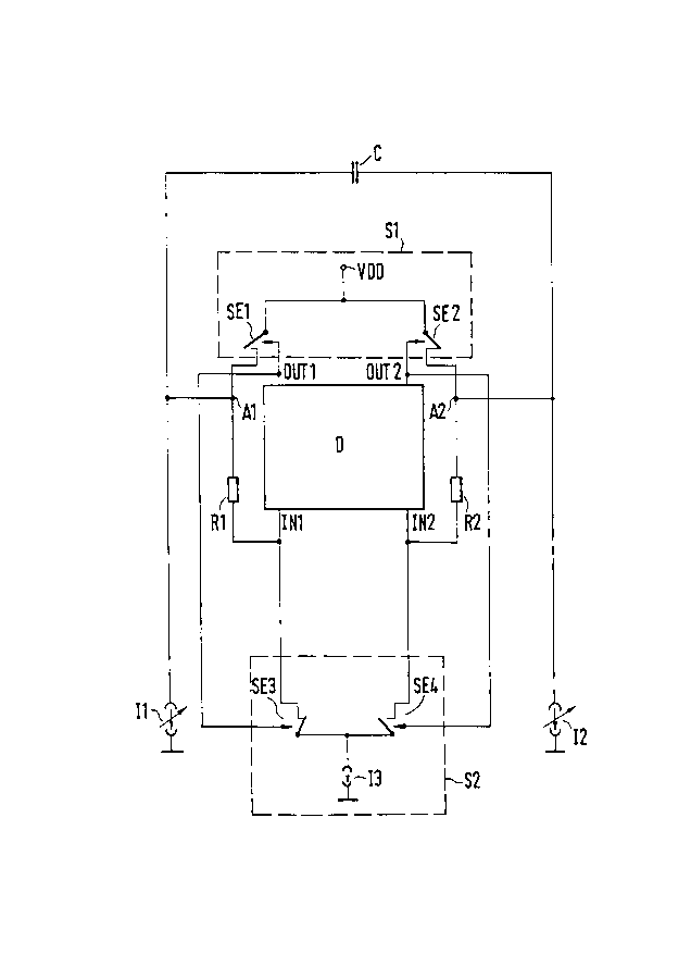
Referring to Fig. 1, a CMOS oscillator in accordance
with the invention comprises a differential amplifier
D, a first switching unit S1 containing a f;rst switch-
ing element SE1 and a second switching element SE2, a
second switching unit S2 containing a third switching
element SE3 and a fourth switching element SE4, a
first controlled current source I1, and a second con-
trolled current source I2. The two controlled current
sources I1, I2 are interconnected via a capacitor C.
The first current source I1 is also connected through
a first resistor R1 to a first input IN1 of the differen-
tial amplifier D, and the second current source I2 is
connected through a second resistor R2 to a second input
IN2 of the differential amplifier D.
A supply-voltage terminal VDD (+5 V) is connectable via
the switching path of the first sw;tching element SE1
to a first tap A1 located between the first current
source I1 and the first resistor R1, or via the switching
- - 2012~
path of the second switching element SEZ to a second tap
A2 located between the second current source I2 and the
second resistor R2.
A first output OUT1 and a second output OUT2 of the
differential amplifier D are connected to a control in- -
put of the first switching element SE1 and to a control
input of the second switching element SE2, respectively.
Either the first input IN1 or the second input IN2 of
the differential amplifier D is connectable to a third
CMOS current source I3 via the switching path of the
third switching element SE3 or via the sw;tching path
of the fourth switching element SE4, respectively. A
control input of the third switching element SE3 and a
control input of the fourth switching element SE4 are
connected to the first output OUT1 and the second output
OUT2, respectively, of the differential amplifier D.
A preferred embodiment of the oscillator according to
the invention will now be described in detail with the
aid of Fig. 2.
The first switching unit S1 consists of a first NMOS
transistor N1, which forms the first switching element
SE1, and a second NMOS transistor N2, which forms the
second switching element SE2, and associated first and
second current mirrors.
- - 2012556
The first current mirror is made up of a first PMOS
transistor P1 and a second PMOS transistor P2. The two
drain terminals are connected to the supply-voltage
terminal VDD. The two gate terminals are connected to-
gether, and the source terminal of the second PMOS
transistor P2 is coupled back to the interconnected
gate terminals and connected to the drain terminal of
the first NMOS transistor N1. The source terminal of the
first PMOS transistor P1 is connected to the first tap
A1.
The second current mirror is made up of a third PMOS
transistor P3 and a fourth PMOS trans;stor P4 and is
symmetrical with respect to the first current mirror.
Accordingly, it is connected to the second NMOS
transistor N2 (source terminal of P3 to drain terminal
of N2) and the second tap A2 (connected to the source
terminal of P4).
The source terminals of the first and second NMOS
transistors N1, N2 are connected together and to the
fourth current source I4. The gate terminals of the
first NMOS transistor N1 and the second NMOS tran-
sistor N2 form the control inputs of the first switching
element SE1 and the second switching element SE2, re-
spectiveLy (cf. Fig. 1).
The second switching unit S2 contains a third NMOS
transistor N3, forming the third switching element, and
a fourth NMOS transistor N4, forming the fourth switch-
ing element. The drain terminal of the third NMOS
2012SS6
_
transistor N3 is connected to that term;nal of the
first resistor R1 which is remote from the first tap
A1, and the drain terminal of the fourth NMOS transis-
tor N4 is connected to that terminal of the second re-
sistor R2 which is remote from the second tap A2. The
source terminals of N3 and N4 are connected together
and to the third current source I3. The gate terminals
of the third NMOS transistor N3 and the fourth NMOS
transistor N4 form the control inputs of the third
switching element SE3 and the fourth switching element
SE4, respectively (cf. Fig. 1).
As shown in F;g. 2, the differential amplifier D is de-
s;gned as a cascaded two-stage amplif;er circu;t. The
first differential-amplfier stage consists of fifth,
sixth, seventh, and eighth NMOS transistors N5, N6, N7,
N8 and a f;fth CMOS current source I5. Analogously, a
second different;al-amplifier stage consists of ninth,
tenth, eleventh, and twelfth NM0S transistors N9, N10,
N11, N12 and a sixth CMOS current source I6.
The drain terminals and the interconnected gate terminals of
N5 and N6 are connected to the supply-voltage terminal
VDD. The source terminals of N5 and N6 form the first out-
put OUT1 and the second output OUT2, resDectively, of
the differential amplifier D (see also Fig. 1). The two
transistors N5, N6 represent the two load resistances of
a conventional differentiaL amplifier. The source terminals
of N7 and N8 are connected together and to the fifth
2012556
current source I5. The drain terminals of N7 and N8 are
connected to the source terminals of N5 and N6, re-
spectively. The gate terminals of N7 and N8 form a
first ~ put and a second ~ put, respectively, of
the first differential-amplifier stage. The two NMOS
transistors represent the f;rst stage of the differen-
tial amplifier.
The second differential-amplifier stage is constructed
anaLogously tothe first differentiaL-amplifier stage,
with the ninth NMOS transistor N9 and the tenth NMOS
transistor N10 representing the two load resistances,
and the eleventh NMOS transistor N11 and the twelfth
NMOS transistor N12 forming the second amplifier stage
(cf. Fig. 2).
.
The drain terminals of N11 and N12 are connected to the
second and first outputs, respectively, of the first
differential amplifier stage. The gate terminals of N11
and N12 form the first input IN1 and the second input
IN2, respectively, of the differential amplifier D.
The first controlled current source 11 and the second
controlled current source I2 are connected together via
the frequency-determining capacitor C. The first cur-
rent source I1 is connected to the drain terminal of N3
through the first resistor R1, and the second current
source I2 is connected to the drain terminal of N4
through the second resistor R2.
2012~6
According to an advantageous aspect of the invention,
the terminal of the first resistor R1 remote from the
first tap A1 is connected to the gate terminal of a
thirteenth NMOS transistor N13, and the terminal of the
second resistor R2 remote from the second tap A2 is
connected to the gate terminal of a fourteenth NMOS
transistor N14. The drain terminals of N13 and N14 are
connected to the supply-voltage terminal VDD. The
source terminal of N13 is connected to the gate ter-
minal of N11, i.e., to the first input IN1 of the
differential amplifier D, and to a seventh CMOS cur-
rent source I7. Analogously, the source terminal of N14
is connected to the gate terminal of N12, i.e., to the
second input IN2 of the differential amplifier D, and
to an eighth CMOS current source 18.
The thirteenth NMOS transistor N13 and the fourteenth
NMOS transistor N14 form source-follower stages whose
input capacitances are lower than those of the subsequent
differential-amplifier transistors N11 and N12, re-
spectively, by about a factor of 5 to 10, so that the
RC products formed via the first resistor R1 and the
second resistor R2 become negligibly small.
The seventh current source I7 and the eighth current
source I8 serve to set the operating points of N13 and
N14, respectively. Through the drive of N13 and N14
with the currents I7 and I8, respectively, gate-to-source
voltages are developed in N13 and N14 which make it
2012~6
.
possibLe to operate the subsequent differential-ampli-
fier transistors N11 and N12 in the pinch-off region
of the transistor characterist;c. Because of its
steeper slope and, hence, higher gain, the pinch-off
region is preferable to the ohmic region of the
characteristic.
A construction of the controlled current source 11, 12
will now be explained with the aid of Fig. 3. The
current source includes two NMOS transistors N15, N16
connected as a current mirror, with N15 forming the
output current path for the second current source. A
seventeenth NMOS transistor N17, whose gate terminal
is connected to the gate terminal of N16, forms the
output current path for the first current source I1.
The output currents 11 and 12 of the two current sources
are proportional to the drive current. To balance the
oscillator, a unity current transfer ratio, i.e.,
equal output currents 11 and I2, are chosen. ~ia the
currents I1 and 12, the oscillator frequency can be
linearly changed.
The oscillator operates off a +5-~ supply. Both re-
sistors R1, R2 have a value of 1 kohm. The two con-
trolled current sources deliver a current in the milli-
ampere range, and the voltage swing of the circuit
(voltage drop across the resistors) is in the range of
a few hundred millivolts. Each of the differential-
2012556
-
- 10 -
amplifier stages has a gain in the range from 2 to 10,
and to achieve frequencies clearly above 100 MHz, the
capacitor C has a capacitance in the picofarad range.
The fourth current source I4 is designed to deliver a
current I4 whose value is slightly greater than the
sum of the values of the first, second, and third
current sources (cf. Fig. 2).
The operation of the oscillator according to the inven-
tion will now be explained with the aid of the timing
diagram of Fig. 4.
The first line - a - shows the waveform of the voltage
UC across the capacitor C. At a first switch point, the
capacitor voltage UC is equal to the voltage drop
across the first resistor R1 (UC = R1 x I3); at a sec-
ond switch point, it is equal to the voltage drop
(swing) across the second res;stor R2 (UC = R2 x I3).
The second line - b - shows the voltage waveform U1Z
between the first and second switching elements SE1,
SE2 of the first switching unit S1 (for U12, see Fig. 2).
In the third line - c -, the voltage swing UR1 at the
first resistor R1 is plotted against time t, and in
the fourth ~ine - d - the voltage swing UR2 at the sec-
ond resistor R2 is plotted against time t.
2012556
- 11 -
The fifth line - e - shows the voltage waveform U87 at
the differential-amplifier inputs IN1, IN2. The time
axes t are divided into the time intervals O, 1/4,
1/2, 3/4, ... of the period T of the oscillator signal
of frequency f. When the circuit is balanced (i.e.,
I1 = I2, R1 = R2), the oscillator frequency f is
f = I1/4 x C x R1 x I3.
Assuming that the capacitor C is uncharged (UC = O)
at an instant t = O (cf. Fig. 4),in a first state, a
first current path consisting of the first current
mirror P1, P2, the first switching element N1 (cf.
Fig. 4b, U12 > O), the first differential-amplifier
stage (N7 conducting), and the second differential-
amplifier stage (N12 conducting) is completed (U 87 > O
in Fig. 4e). As a result, the third switching element
SE3, i.e., the third NMOS transistor N3, is ON, so that
a voltage UR1 = I3 x R1 (cf. Fig. 4c) appears across
the first resistor R1. Since the fourth NMOS transistor
N4 (cf. Fig. 2) is OFF in the first state, and on condi-
tion that N13 and N14 are identical and, thus, have the same
gate-source voltage drop, at the instant t = O, the
voltage drop UR1 across the first resistor R1 is equal
to the voltage drop U87 between the differentia[-ampli-
fier inputs (cf. Figs. 4c and 4e).
With P1 conducting and P4, i.e., the second current
mirror, cut off (U12 > O), the capacitor C is now charged
201255~
by the current I2 from the second current source I2
(cf. Fig. 4a). Accordingly, the voltage U87 between
the differential-amplifier inputs decreases (cf. Fig.
4e), namely untiL the capacitor voltage UC is equal to
the value UR 1 = R1 x I3 and U87 = 0 at the instant t = T/4
(cf. Figs. 4a, 4e).
The circuit now changes to the second state. Since now
U12 ~0, the first current path is blocked and a sec-
ond current path, consisting of the second current
mirror P3, P4, the second NMOS transistor N2, i .e.,
the second switching element SEZ, the first differen-
tial-amplifier stage (N8 conducting), and the second
differential-amplifier stage (N11 conducting), is
completed (cf. Figs.4b, 4e, since U87 < O). The
voltage drop across the second resistor R2 is now UR2
= U2 x I3 (cf. Fig. 4d).
The capacitor C is thus discharged (cf. Fig. 4a) until
its voltage UC = -URZ = -R2 x I3 at the instant
t = 3 T/4 (cf. Fig. 4a), so that the circuit changes
back to the first state (cf. Fig. 4b,now U12 > 0,
Fig. 4c,now UR1 = R1 x I3), and reaches the initial
state, i.e., UC = O, at the instant t = T. The oscil-
lator cycle just described then repeats itself.
The oscillator described can be used between very low
frequencies and about 200 MHz. It permits linear con-
trol of the output frequency within wide limits. Com-
pared with conventional bipolar oscillators, it has very
2012~5~
low power consumption and considerably higher accuracy.
Compared with conventional CMOS oscillators,it ex-
hibits much better temperature and parameter stability
because of its simple symmetrical construction, since
the individual factors of influence cancel each other.
In addition, a frequency range higher by the first
power of ten is adjustable.
A particular advantage of this CMOS circuit lies in the
fact that it is suitable for impLementation on large-
scale integrated-circuit chips,which hitherto needed
additional external bipolar voltage-controlled
oscillators (VCO) to achieve the necessary accuracy
and the very high frequencies.
It is also possible, of course, to construct the oscil-
Lator with transistors of reverse conductivity
(i.e., to replace PMOS transistors by NMOS transistors,
and vice versa).