Note : Les descriptions sont présentées dans la langue officielle dans laquelle elles ont été soumises.
2~12~g8
-- 1 --
FT~ER OPTIC GYRO
BACKGROUND OF THE INVENTION
The present invention relates to a closed-loop-
type zero-system fiber optic gyro.
A wide-dynamic-range, low-drift fiber optic
gyro that has been proposed in the past has an
arrangement in which a phase modulator, formed as an
optical modulator, is provided at one end of an optical
fiber coil, a ramp voltage for phase modulation is
applied to the phase modulator to provide a phase
difference between two rays of light propagating through
the optical fiber coil, a phase difference between two
rays of lLght which propagate through the optical fiber
coil and interfere with each other is detected from the
output of a photodetector, and the polarity and frequency
of the ramp voltage are controlled by the detected output
so that the phase difference is 2m~ rad (where m = 0,
+ 1, + 2, ..... ..............), or zero (m = 0), in general.
Fig. 1 illustrates an example of such a
conventional closed-loop-type, zero-method fiber optic
gyro of a linear phase ramp method which employs a ramp
Yoltage for phase modulation. Light 12 from a light
source 11 is applied via an optical coupler 13 and a
polarizer 14 to an optical splitter/coupler 15, by which
the light 12 is split into two rays of light 16a and
16b. The two rays of li~ht 16a and 16b enter an optical
fiber coil 17 at one and the other end 17a and 17b
thereof, respectively, and propagate therethrough as
left-handed and right-handed light 17a and 17b, there-
after being emitted therefrom as rays of light 18a and
18b. ~hese rays of light 18a and 18b are supplied to the
optical splitter/coupler 15, wherein they interfere with
~*
~ 20~27~8
each other, and the resulting interference light 19 is
applied via the polarizer 14 and the optical coupler 13
to a photodetector 21, whereby it is converted into an
electric signal. On the other hand, a phase modulator 22
is provided between the optical splitter/coupler 15 and
the terminating end 17b of the optical fiber coil 17 and
is supplied with a bias voltage Bi from a bias voltage
generator 23. Consequently, the light 16b which enters
the optical fiber coil 17 at the terminating end 17b and
the light 18a which is applied from the terminating end
17b of the optical fiber coil 17 to the optical splitter/-
coupler 15 after having propagated through the coil 17
are phase-shifted relative to each other. Further, a
phase modulator 24 is provided between the optical
splitter/coupler 15 and the terminating end 17a of the
optical fiber coil 17 and is supplied with a ramp voltage
Rp from a ramp voltage generator 30. Consequently, the
light 16a which enters the optical fiber coil 17 at its
terminating end 17a and the light 18b which is applied
from the terminating end 17a of the optical fiber coil 17
to the optical splitter/coupler 15 after having propagated
through the coil 17 are phase-shifted. The output
voltage Va of the photodetector 21 is provided to a
synchronous detector 41 which forms a phase difference
detect and control circuit 40 and in which it is
synchronously detected by the bias voltage Bi from the
bias voltage generator 23. As a result of this, a
voltage Vb which corresponds to the phase difference
~ ~ between the two rays of light 18a and 18b coupled
together by the optical splitter/coupler 15 is detected by
the synchronous detector 41 and is applied to a PID
(Proportional plus Integral plus Derivative) filter 42.
The output voltage o~ the PID filter 42, that is, the
` r~ 20127~
-- 3 --
output voltage Vo of the phase difference detect and
control circuit 40, is supplied to the ramp voltage
generator 30, controlling the polarity and frequency of
the ramp voltage Rp so that the phase difference ~ ~ is
reduced to zero.
The phase modulaiion in the phase modulator 22
by the biasing voltage Bi is intended to set the
operation point of the fiber optic gyro so that the
output voltage Vb of the synchronous detector 41 becomes0 proportional to the sine value of the phase difference
as follows.
Vb = Ksin ~
where K is a constant.
The phase difference ~ ~ is expressed as the
sum of a Sagnac phase difference ~ ~ . resulting from
the application of angular velocity Q to the optical
fiber coil 17 and a phase difference ~ ~ ~ resulting from
the application of the ramp voltage Rp to the phase
modulator 24 as follows:
a ~ . (2)
As is well-known, the Sagnac phase difference ~ ~ , is
expressed as follows:
4~ RL
. = Q (3)
~ C
where R is the radius of the optical fiber coil 17, L is
the length of tne optical fiber coil 17, ~ is the
wavelength of light which propagates through the optical
fiber coil 17 and C is the light velocity in a vacuum.
The ramp voltage Rp is a positive or negative
sawtooth voltage as shown at the upper left or right-hand
side in Fig~ 2, and a maYimum or minimum value of the
ramp voltage corresponding to its peak value is selected
~ 2~2~
such that the width of the phase shift ~ ~ of light by
the phase modulator 24 is 2k~ rad (where k = + 1, + 2,..),
in general and usually + 2 ~ rad.
For example, where the input angular velocity
~2 is applied in the left-handed direction and the Sagnac
phase difference ~ ~ . goes negative, the ramp voltage
Rp is controlled to be a positive sawtooth voltage by the
output voltage Vc of the phase difference detect and
control circuit 40. In this instance, the phase shift
~ ., which is caused by the phase modulator 24 in the
light 16a which enters the optical fiber coil 17 at its
terminating end 17a, and the phase shift ~ ~, which is
caused by the phase modulator 24 in the light 18b which
is applied to the optical splitter/coupler 15 from the
terminating end 17a of the optical fiber coil 17 after
propagating therethrough, bear such a relationship as
indicated by the solid and broken lines at the lower
left-hand side in Fig. 1, and the phase difference ~ ~ ~
which results from the application of the ramp voltage Rp
to the phase modulator 24 goes positive. Where the input
angular velocity Q is applied in the right-handed
direction and the Sagnac phase difference ~ ~ . goes
positive, the ramp voltage Rp is controlled to be a
negative sawtooth voltage by the output voltage Vc of the
phase difference detect and control circuit 40. In this
instance, the above-mentioned phase shifts ~ , and ~ ~
bear such a relationship as indicated ~y the solid and
broken lines at the lower right-hand side in Fig. 2, and
the above-mentioned phase difference ~ ~ ~ goes
negative. In Fig. 2, l is the time necessary for the
propagation of light through the optical fiber coil 17.
Thus, letting the period and frequency of the
ramp voltage Rp be represented by T and f, respectively,
~^~ 20127~8
it follows that
1:
p = 2k ~ = 2k~ f (4)
T
as is evident from Fig. 2.
Letting the refractive index of light in the optical
fiber coil 17 be represented by n, the following
relationship exists:
nL
C
Hence, it follows that
nL
~ ~ p = 2k~ f (6)
Thus, by controlling the polarity and frequency f of the
lamp voltage Rp so that the phase difference
expressed by Eq. (2) is reduced to zero, it ~ollows,
from Eqs. (6) and (3) and ~ , that
C
f = ~ ~ P
2k~ nL
C
2kn nL
C 4~ RL
= _ Q
2k~ nL a c
2R
= - Q (7)
kna
The input angular velocity Q is given as follows:
~ 2012~88
kn ~
2R f (a)
1n the case where the input angular velocity Q is
applied in the left-handed direction, i.e. the negative
direction and the ramp voltage Rp becomes a positive
sawtooth voltage, however, k becmes a positive integer,
and in the case where the input angular velocity Q is
applied in the right-handed direction, i.e. the positive
direction and the ra~.p voltage Rp becomes a negative
sawtooth voltage, k becomes a negative integer.
Thus, the direction and magnitude of the input
angular velocity Q can be measured from the polarity and
frequency f of the ramp voltage Rp.
The phase modulator 24 usually has an optical
waveguide formed as by diffusing titanium into an
electro-optic crystal as of lithum niobate and a pair of
electrodes across which voltage for modulation use is
applied. The phase shift amount of light by such a phase
modulator is proportional to the product r vp of the
electro-optic constant r of the. electro-optic crystal
and the applied voltage Vp. The electro-optic constant
~ is temperature dependent and has a temperature
co-efficient of about 500 ppm/C though somewhat
different according to the direction of cut of the
electro-optic crystal. Accordingly, the phase shift
amount of light in the phase modulator varies with
temperature, even if the applied voltage Vp is constant.
In the prior art fiber optic gyro described
above with respect to Fig. 1, a maximum or minimum value
of the ramp voltage Rp which is applied to the phase
modulator 24 from the ramp voltage generator 30 is fixed
at such a value that a maximum phase shift of light in the
~` 20~27g8
phase modulator 24 by the ramp voltage Rp is 2k~ rad at
a specified temperature of 15C, for e~ample. Hence, ~f
the temperature of the fiber optic gyro, and consequently
the temperature of the phase moduiator 24 deviates from
S the specified temperature owing to an environmental
change, the electro-optic constant r of the electro-
optic crystal forming the phase modulator 24 changes,
resulting in the maximum phase shift deviating from 2 k ~
rad. In consequence, the relationship ~etween the input
angular velocity Q and the frequency f of the ramp
voltage Rp, defined by Eq. (7) or t8) is lost, inducing a
scale factor error in the output of the fiber optic gyro.
Fig. 3 shows the scale factor error in the
conventional fiber optic gyro in the case where the peak
value of the ramp voltage Rp was set so that the ma~imum
phase shift would be + 2 ~ rad at 15'C. When the
temperature of the fiber optic gyro is 15 + 70~C, that
is, +85-C or -55-C, the maximum phase shift deviates
about 3.5% from + ~ ~ rad and the scale factor error is
as large as approximately 0.06%. In the case where the
ramp voltage Rp is a sawtooth voltage as mentioned above,
however, a fly-back time exists in the sawtooth voltage,
in practical; strictly speaking, Eq. ~4) does not hold at
a specified temperature and a scale factor error occurs
~5 in the output of the fiber optic gyro. Fig. 3 shows the
case where the flyback time of the ramp voltage Rp was
selected as short as ;0 nanosec so that the scale factor
error by the flyback time of the ramp voltage Rp would be
negligibly small. Hence, the scale factor error shown in
Fig. 3 is almost due to the deviation of the ma~imum
phase shift from + 2 ~ rad.
SUMMARY OF THE INVENTION
~` 201'~7~8
-- 8 --
It is therefore an object of the present
invention to provide a ciosed-loop-type, zero-method
fiber optic gyro in which substantially no scale factor
error is induced in its output by a temperature change in
the constant of the phase modulator when the temperature
of the fiber optic gyro stays within a predetermined
temperature range.
The closed-loop-type, zero-method fiber optic
gyro according to the present invention includes a
temperature sensor for sensing the temperature of the
gyro, and peak value control circuit which controls the
peak vaiue of the ramp voltage according to the output of
the temperature sensor so that the maximum phase shift of
light in the phase modulator supplied with the ramp
lS voltage is an integral multiple of 2~ rad regardless of
the temperature of the gyro when it stays within a
predetermined temperature range.
According to such a fiber optic gyro of the
present invention, since the peak value of the ramp
voltage is controlled so that the ma~imum phase shift of
light in the phase modulator supplied with the ramp
voltage is an integral multiple of 2~ rad within a
predetermined temperature range regardless of the
temperature of the gyro, its output is almost free from
scale factor errors by a temperature change in the
constant of the phase modulator supplied with the ramp
voltage.
~RIEF DESC~IPTION OF THE DRAWINGS
~0 Fig. 1 is a block diagram showing a conventional
fiber opt_c gyro;
Fig. 2 is a ramp voltage waveform diagram for
explaining the operation of the fiber optic gyro depicted
9 20~2~
in Fig. 1;
Fi~, 3 is a graph showing a scale factor error
by the fiber optic gyro depicted in Fig. l;
Fig. 4 is a block diagram illustrating an
embodiment of the fiber optic gyro of the present invention;
Fig. 5 is a graph showing the relationship
between temperature and a correction voltage in the
em~odiment of Fig. ~;
Fig. 6 is a waveform diagram for e~plaining the
correction of the peak value of the ramp voltage;
Fig. 7 is a block diagram illustrating another
embodiment of the fiber optic gyro; and
Fig. 8 is a block diagram showing a modi~ied
form of a peak value control circuit 60.
DESCRIPTION OF THE PREFERRED EMBODIMENTS
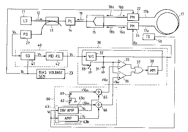
Fig. 4 illustrates in block form an embodiment
of the fiber optic gyro of the present invention, which
is of a,linear phase ramp method employing a ramp voltage
for phase modulation. This embodiment is identical with
the prior art example of Fig. l in the provision of the
light source 11, the optical coupler 13, the polarizer
14, the optical splitter/coupler 15, the optical fiber
coil 17, the photodetector 21, the phase modulator 22
which is supplied with the bias voltage Bi, the bias
voltage generator 23, the phase modulator 24 which is
supplied with the ramp voltage Rp, the ramp voltage
generator 30 and the phase difference detect and control
circuit 40. The operation principle of this embodiment
is also identical with the operation principle of the
prior art e~ample e~cept that the peak value of the ramp
voltage Rp is controlled as described later.
The phase modulator 24 is formed of an
~` 2~1273~
-- 10 --
electro-optic c~ystal where electro-optic constant r
has a positive temperature coefficient, such as lithium
niobate, in this example.
~ he ramp voltage generator 30 in this e~ample
comprises a capacitor 31, a voltage-current converter 32
whereby the output voltage Vc, which is the input voltage
to the ramp voltage generator 30, is converted into a
current for input into the capacitor 31, a switch 33 for
discharging the capacitor 31, a voltage comparator 35 for
comparing the charging voltage of the capacitor 31 with a
positive reference voltage +Vpr, a voltage comparator 36
for comparing the charging voltage of the capacitor 31
with a negative reference voltage -Vmr, an OR gate 37 for
ORing the outputs of the voltage comparators 35 and 36,
and a monostable multivibrator 38 which is triggered by
the output of the OR gate 37 to hold the switch 33 in the
ON state for a short time. When the output voltage Vc of
the phase difference detect and control circuit 40 is
positive, the capacitor 31 is charged positive, and when
the charging voltage reaches the reference voLtage +Vpr,
the output of the voltage comparator 35 and consequently
the output of the OR gate 37 goes high, triggering the
monostable multivibrator 3~. As a result of this, the
switch 33 is held ON for a short time, during which the
capacitor 31 is discharged, and thereafter it is charged
again. Thus, a positive sawtooth voltage whose masimum
value is equal to the reference voltage +Vpr, is
developed as the ramp voltage Rp across the capacitor
31. When the output voltage Vc of the phase difference
detect and control circuit g0 is negative the capacitor
31 is charged negative, and when the charging voltage
reaches the reference voltage -Vmr, the output of the
voltage comparator 35 and consequently the output of the
~ 2~
11 --
OR gate 37 goes high, triggering the monostable multi-
vibrator 38. As a result of this, the switc~ 33 is held
ON for a short time, during which the capacitor 31 is
discharged, and thereafter it is charged again. Thus, a
negative sawtooth voltage whose minimum value is equal to
the reference voltage -Vmr, is developed as the ramp
voltage Rp across the capacitor 31.
In this instance, a switching element which is
sufficiently small both in the leak current during its
OFF state and in the resistance during its ON state, such
as a field effect transistor, is employed as the switch
33. Further, the time constant of the monostable
multivibrator 38 is set such that the ON-state period of
the switch 33, that is, the flyback period of the ramp
voltage Rp is sufficiently short, for e~ample, SO nsec or
so .
The present invention employs a temperature
sensor 50 and a peak value control circuit 60.
The temperature sensor 50 is to detect the
temperature of the fiber optic gyro, in particular, the
temperature of the phase modu}ator 24. The temperature
sensor 50 may preferably be disposed near the phase
modulator 24 but may also be located at some other place
where temperature is ~early equal to that of the phase
modulator 24. Now, let it be assumed that the temperature
of the fiber optic gyro varies within a range from -54-C
to +85-C according to environmental conditions. The
temperature sensor 50 is designed so that its detected
voltage Vt varies linearly with temperature, for eYample,
zero (the ground potential) at a reference temperature
25-C, positive above 25-C and negative below 25'C as
shown in Fig. 5.
The peak value control circuit 60 ~s to control
- 20127~8
- 12 -
the peak value of the ramp voltage Rp according to the
above temperature detected voltage Vt so that the maximum
phase shift of light in the phase modulator 24 is 2k~ rad
(where k = 1, ~ 2, ...), i.e. + 2 ~ rad in this
e~ample, regardless of the temperature of the fiber optic
gyro when it stays within a predetermined range, that is,
within a ra~ge of from -54 to +85C in this example. The
peak value control circuit 60 in this embodiment is made
up of a voltage source 61 for providing a positive
voltage ~Vpo, a voltage source 62 for providing a negative
voltage -Vmo, a correction voltage generator 63 for
deriving correction voltages Vx and Vy, described later,
from the detected voltage Vt, an adder 65 for adding the
correction voltage VY to the voltage +Vpo, and an adder
66 for adding the correction voltage Vy to the voltage
-Vmp. The correction voltage generator 63 includes an
inverting amplifier for amplifying the detected voltage
Vt in the reverse polarity to provide the correction
voltage VY and an amplifier 63b for amplirying the
detected voltage Vt to provide the correction voltage Vy.
Provision is made for adjusting the gain of at least one
of the amplifiers 63a and 6~b so that the correction
voltages V~ and Vy depicted in Fig. are opposite in
gradient (opposite in PoLaritY) and equal in magnitude.
The output voltages of the adder 65 and 66 are used as
the reference voltages +Vpr and -Vmr which are applied to
the voltage comparators 35 and ~6 of the ramp voltage
generator ~0.
In Fig. 4 the gain of each of the adders 65 and
66 may be 1. In such a case, when the temperature of the
fiber optic gyro is 25-C which is the reference tempera-
ture, the correction voltages VY and Vy are zero as
described later and the voltages +Vpo and -Vmo are
~ .
,
.
20~27~8
- 13 -
provided intact as the reference voltages +Vpr and -Vmr
to the voltage comparators 35 and 36. Consequently, the
peak value or maximum value of the positive ramp voltage
Rp is the voltage +Vpo and the minimum value of the
negative ramp voltage Rp is the voltage -Vmo. These
voltage values are selected such that maximum phase shifts
of light by the phase modulator 24 are +2 ~ rad and
-2~ rad, respectively.
The correction voltage V~ is for correcting the
posltive ramp voltage Rp and varies linearly as shown in
Fig. 5, in which the voltage V~ is zero when the detected
voltage Vi from the temperature sensor 50 is zero, that
is, the temperature of the fiber optic gyro is 25C, and
the voltage Vx goes negative and positive when the
temperature of the fiber optic gyro is above and below
25C, respectively. In other words, the voltage Vx is
proportional to the detected voltage Vt but opposite in
polarity. The values of the voltage Vx is selected such
that when the electro-optic constant y of the
electro-optic crystal forming the phase modulator 24
varies with temperature, the resulting change in the
phase shift amount of light in the phase modulator 24 is
cancelled.
The correction voltage Vy is for correcting the
negative ramp voltage Rp and is proportional to the
detected voltage Vt in the same polarity as shown in Fig.
5. The value of the voltage Vy is selected such that
when the electro-optic constant r of the electro-optic
crystal forming the phase modulator 24 changes with
temperature, the resuiting change in the pahse shift
amount of light in the phase modulator 24 is cancelled.
In the case where the Sagnac phase difference
, is negative and the output voltage Vc of the phase
2~12~8
- 14 -
di~ference detect and control circuit 40 is positive and
consequently a positive ramp voltage Rp is being
generat~d, the peak value of the ramp voltage Rp is the
sum of the volta~e +Vpo and the correction voltage Vx as
~epicted at the left-hand side in Fig. 6. Accordingly,
the maximum value of the ramp voltage Rp is corrected so
that the maximum phase shift of light in the phase
modulator 24 is always +2 ~ rad even if the temperature
of the fiber optic gyro varies within the afore-mentioned
range from -54C to +85C. In the case where the Sagnac
phase difference ~ ~ ~ is positive and the output
voltage Vc of the phase diEference detect and control
circuit 40 is negative and consequently a negative
sawtooth voltage is being generated as the ramp voltage
Rp, the peak value or minimum value of the ramp voltage
Rp is the sum of the voltage -Vmo and the correction
voltage Vy as depicted at the right-hand side in Fig. 6.
Accordingly, the peak value of the ramp voltage Rp is
corrected so that tne maximum phase shift of light in the
phase modulator 24 is .always -2 ~ rad even if the
temperature of the fiber optic gyro varies within the
afore-mentioned range from -54C to +85C. ~y measuring
the polarity and frequency f of the thus obtained ramp
voltage Rp through use of a known method, the direction
and magnitude of acceleration applied to the optical
fiber coil 17 can be calculated from Eq. (8). No
particular method for measuring the polarity and
frequency of the ramp voltage Rp is described and shown,
because any known methods can be used. As described
above, no scale factor errGr is induced in the output of
the fiber optic gyro by a temperature change in the
electro-optic constant y of the electro-optic crystal
forming the phase modulator 24.
20~ 2~8
- 15 -
In the above, however, since the correction
voltages Vx and Vy are set on the assumption that the
temperature detected by the temperature sensor 50 is e~ual
to the temperature of the phase modulator 24, when the
temperature sensed by the temperature sensor 50 differ~
from the temperature of the phase modulator 24, the
maximunt phase shift of light in the phase modulator 24
deviates from + 2 ~ rad and a temperature change in the
electro-optic constant r of the electro-optic crystal
lG forming the phase modulator 24 will induce a scale factor
error in the output of the fiber optic gyro. In practice,
however, the difference between the temperature sensed
by the temperature ~ensor 50 and th~ temperature of the
phase modulator 24 is so small that the maximum phase
shi f t of light in the phase modulator 24 remains
substantially equal to + 2 ~ rad, and hence the result-
ing scale factor error is very slight.
The peak value control circuit ~0 may be of an
arrangement ln which the afore-mentioned reference
voltages +Vpr and -Vmr are derived directly from the
detected voltage Vt oF the temperature sensor 50.
Moreover, the PID filter 42 in the phase difference
detect and control circuit 40 may be replaced with an
electric filter having the same function.
Fig. 7 illustrates in block fornt another
embodiment of the fiber optic- gyro of the present
invention, in which the analog ramp voltage generator 30
used in the Fig. 4 embodiment is substituted with a
digital ramp voltage generator 30 which uses a staircase
wave.
The digital ramp voltage generator 30 comprises
an AD converter 73 for converting the output voltage Vc
of the phase difference detect and control circuit 40
2~27~8
; into a digital value Dc, a digital ramp voltage generator
71 for generating a digital ramp voltage Dp which uses
the digital value Dc as its step width, a DA converter 72
for converting the digital ramp voltage Dp into an analog
S ramp voltage Rp, and a clock generator 74 for applying an
operation clock CL to the AD converter 73, the digital
ramp voltage generator 71 and the DA converter 72. The
digital ramp voltage generator 71 includes an adder/-
subtrator 71a which is supplied at one input with the
output Dc of the AD converter 73 and a latch 71b for
holding the output of the adder/subtractor 71a. The
output of the latch 71b is provided to the DA converter
72 and the other input of the adder/subtractor 71a. The
adder/subtractor 71a is switched between additive and
subtractive operations by a sign bit S in the output of
the AD converter 73, namely, the adder/subtractor 71a
performs subtraction or addition depending on whether the
sign bit S is a "0~ or "ln, for instance.
When the output voltage Vc of the phase
difference detect and control circuit 40 is applied to
the digital ramp voltage generator 30 constructed as
described above, the voltage Vc is converted by the AD
converter 73 into the digital voltage value Dc upon each
occurrence of the clock CL. The digital voltage value Dc
is provided to the adder/subtractor 71a, together with
the sign bit S, by which its addition to or subtraction
from the output Dp of the latch 71b, which has latched
therein the output of the adder/subtractor 71a one clock
before, is performed in accordance with the state of the
sign bit S for each clock. For instance, in the case
where the input voltage Vc is positive, and hence the
slgn bit S output from the AD converter 73 is a "1~, the
digital voltage value Dc and the output value Dp of the
- 2~ ~7~
- 17 -
latch 71b are added together by the adder/subtractor 71b,
the added result is latched in the latch 71b, from which
it is output upon the ne~t occurrence of the clock CL.
In consequence, the output of tXe latch 71b gradually
increases by a step of the value Dc upon each occurrence
of the clock CL. Yet, when the sum of the latest output
value Dp of the latch 71b and the input digital value Dc
exceeds a ma~imum value dependent upon the number of
digital (or the number of bits) of the adder/subtractor
71a acting as an adder, the carry is discarded, and
consequently, the output of the adder/subtractor 71a goes
down to a value smaller than the value Dc. Then the
cumulative addition by the step of the value Dc is
performed again by the combination of the adder/subtractor
71a and the latch 71b upon each occurrence of the clock
CL, starting from the above-said reduced value. ln other
words, the digital ramp voltage generator 71 creates a
digital ramp voltage which sequentially increases
stepwise by the value Dc. The ma~imum value of the ramp
voltage Rp is dependent on the number of bits of the
adder/subtractor 71a. Also in the case where the
adder/subtractor 71a operates as a subtractor, a negative
stair step digital ramp voltage is simiiarly produced.
The output voltage Dp of the digital voltage
~enerator 71 is applied to the phase modulator 24 after
being converted by the DA converter 72 into the analog
voltage Rp. In this case, the output volt-age VR of the
pea~ value control circuit 60 is applied as an analog
~0 reference voltage of the DA converter 72. The DA converter
72 is a multiplying type DA converter, which outputs an
analog vo tage which is equal to the product of the input
digital value Dp and the analog reference voltage VR. Since
20~2~8
- 18 -
the analog reference voltage VR output from the peak value
cont-ol circuit 60 varies with the detected voltage Vt
of the temperature sensor 50, the output voltage of the
DA converter 72, that is, the ramp voltage Rp, also
varies, and consequently, the peak value of the ramp
voltage Rp also varies correspondingly. The peak value
control circuit 60 is designed for adding and amplifying
a reference voltage Er from reference voltage source 60e
and the detected voltage Vt from the temperature sensor
50. In this embodiment, letting the resistance values of
a feedback resistor 60f and input resistors 60r and 60t
be represented by Rf, Rr and Rt, respectively, and
assuming that the gain of an operational amplifier 60a is
very large, the output voltage VR of the adder/amplifier or
peak value control clrcult 60 is substantially expressed
as follows:
VR = -{(Rf/Rr).Er + (Rf~Rt).Vt},
where (Rf/Rr) Er corresponds to the voltage Vpo or Vmo in
the peak value control circuit 60 in Fig. 4 and
(Rf~Rt) Vt corresponds to the correction voltage Vx or
Vy. ~y a suitable selection of the value of Rf/Rt, the
slope of the voltage VY or Vy shown in Fig. 5 can be set
as desired. Further, the center temperature in the
operation temperature range can be set as desired by a
æultable selection of the value of (Rf/Rr). Incidentally,
the same circuit arrangement as the adder/amplifier 60
including the operational amplifier 60a and the resistors
60f, 60r and 60t can be used as each of the adders 65 and
66 in the peak value control circuit 60 shown in Fig. 4.
In the embodiment depicted in Fig. 7, the peak
value control circuit 50 may have such an arrangement as
shown in Fig. 8. In this instance, the relationship
between the detected voltage Vt of the temperature sensor
20~ 2~8
.. -- 19 --
50 and the output voltageR V of the peak value control
circuit 60 is prestored in a memory 68, the detected
voltage Vt is converted by an AD cconverter 67 into a
digital value Dt for input as an address into the memory
68 to read out therefrom the corresponding digital value
DR ~ which is converted by a DA converter 6~ into an
analog voltage for use as the output volta~e V of the
peak value control circuit 60. With the use of the
memory 68, it is possible to perform not only a
correction linearly approximate to temperature as by the
correction voltages Vx and Vy but also a correction with
more accurate curves. It is apparent that the peak value
control circuit 60 in Fig. 4 may be implemented by such a
memory which has stored therein correction
characteristics for temperatrue.
Also in the embodiment shown in Fig. 7, the
peak value of the ramp voltage Rp can be controlled
according to the detected voltage Vt of the temperature
sensor 50 so that the maximum phase shift of light in the
phase modulator 24 is + 2 ~ rad regardless of the
temperature of the fiber optic gyro as long as it stays
within the aforementioned range of from -54-C to +85C.
Accordingly, also in this embodiment, the output of the
fiber optic gyro is almost free from the scale factor
error by a temperature change in the electro-optic
constant r Of the electro-optic crystal forming the
phase modulator 24.
The PID filter 42 may be replaced with an
electric filter which has the same function as the filter
42, and the function of the PID filter 42 or electric
filter may he performed ln the digital ramp voltage
generator 71.
~ 2~27~
- 20 -
As described above, the present invention
includes the temperature sensor for sensing the temperature
of the fiber optic gyro and the peak value control
circuit which controls the peak value of the ramp voltage
S so that the maximum phase shift of light in the phase
modulator supplied with the ramp voltage is an integral
multiple of 2 ~ rad regardless of the temperature of the
fiber optic gyro when it stays within a predetermined
temperature range. This ensures that substantially no
scale factor error is induced in the output of the fiber
optic gyro by a temperature chanye in the constant of the
phase modulator when the temperature of the fiber optic
gyro is withing the predetermined range.
It will be apparent that many modifications and
variations may be effected without departing from the
scope of the novel concepts of the present invention.
2S