Note : Les descriptions sont présentées dans la langue officielle dans laquelle elles ont été soumises.
~O~J~~
'I' I'I'LE OF THE I NVENTI ON
Clock extracting cirr_uit. in digital-line signal
receiver
BACKGRC)UND OF THE INVENTION
1. Field of the Invention
The present invention relates to a clock
extracting circt.tit in a. digital-line signal receiver
~chich is used in an electronic exchange connecl.ed t.o an
integrated services digital network (ISDN) or the like
digital line network to extract a clock signal from the
da.t.a of a signal received from the digital 1 ine
network, the clock signal being used to sample the c_la.t.a
of the signal therefrom and more particularly, to 'a
circuit which can realize extraction of aclock signal
with a small-scaled circuit configuration and with
stability and accuracy at all times.
2. Description of the Related Art.
In an electronic exchange having a slave
synchronization type~of interface such as a first-order
group interface in the ISDN, the satnpl ing of a data
signal received from the ISDN requires the eltraction
of a clock signal having a period corresponding to a
data communication rate from the data signal.. Such a
first-order interface is provided for each of the trunk
cirr_uits within a private branch exchange.
An internal configuration of such a first-order
group interface 1 in the ISDN is exemplified in Fig. 1.
The first-order group interface 1 is connected through
1
2~~.~~
a network terminating unit (DSU, not shown) to an TSDN
1 i ne.
As shown in Fig. l, the first-order group
inter~fac:e lincludes signal traxlstnitting~ a.r~d re~~eiviug
transformers 2 a.nd 3 connected to the DSLJ, a sigwa.l
t.ra.nsmit.ting circuit 4 for transmitting a, transnrissiorr
data, a signal receiving circuit 5 for r-eceivirrg d.at.a
rrc_~m the ISl)N and extracting from the received data a
clock signal CLlis for sampling of the received data, a.
clocvk generating circuit 6 for generating various clock
signals ~ l, d~ 2, . . . to be controllably used to absorb a
phase di f ference or j fitter between a speech-c:Lrarrrre l
h i ghsvay 10 i n the exchange and the DSU on tire ba.s i s of
tlrP extracted clock signal CLKs and also for generating
a clock signal CLh to be used for a time-divisional
switch. "la.yer 1" interface I for transfer of data or
control information between the speech-channel highway
10 and a control highway 11 within the exchange, a
central control circuit 8 for receiving from the
i nterface 7 data on a D channe 1 i n the channe 1
structure of "23B + D" or "30B + D" and for perfornring~
protocol control of higher layers than the "las-er 1" to
perform transfer of the control data. bet=tveen the
control highway 11 and the control circuit 8, and a.n
elastic memory 9 for absorbing the phase difference or
fitter occurred when transmitting data between the
speech-channel highway 10 and the DSLI.
Explanation will next be briefly made by also
2
2~~~3
referring to Fig. 2 as to the operation of the signal
receiving circuit 5 whicln mainly ext.ract.s ttoe clock
s i gna 1 on the bas i s of the data of the s i gna.l I-ece i ved
at, the first-orde~~ group interface 1 for the purpose of
sampling the data of the received signal.
A data. to be transmitted from terminals ~I'x7, ancJ
TxR. of the transmitting transformer 2 and a. data. to lie
rf,ceived at. terminals RxT and RxR of the receiving
t.ra.nsformer 3 are respectively made usually in the form
of such an a 1 ternate mark i nvers i on (A141I ) code hav i nti
logical levels "U" and "1" a.s expressed in, e. g. , Fig.
2(a).
The signal receiving circuit 5, when rE:ceiviug~ a
data of such AMI code configuration through the
receiving transformer 3, generates signals RxA and Rxl-3
in which logical level "U" zones correspond to zones
defined by polarity changes in the level of the
received data signal as shown in Fig. 2(b) and (e), a.nd
farther generates such a. signal CLKi as shown in Fig.
2(d) corresponding to a logical sum of these generated
signals RxA and RxI3 (more precisely, by logically
inverting them, that is, corresponding to a NAND
condition). The data level of the signal CLKi is not.
varied in logical level "0" zones. For the purpose of
alternately changing the logical level of the signal
CLKi a.t a predetermined period even in the logical
level "U" zones, a signal having a predetermined period
corresponding to the alternate period of the signal
3
2~~~~~
C'l_.I~i i s separately generated, that is, sc.rch a signal
CL:Its as shown in Fig. 2(e) is even-tuallv ~encrat.ed a.t
the signal receiving circuit. 5. 'fhe signal CLlis thus
generated is outputted from tree circuit 5 tct the clock
~;ener,ating circuit 6 a.s a clock signal e~tract.ed from
the received data signal.
In this way, the signal receiving circuit. 5, even
there is a level non-change region in t.le received data
signal of the AMI code configuration. acts to acquire
the clock signal CLIss a.s its ext.ract.ion clock which
a1 i ern;~t.es always at. the predeterminec.l period
corrres~>ond i ng t.o the commun i cat i on rate of the: data.
I~ ig. 3 i s an exampl a c>f the conf i gt~ra-t. i on of the
prior art signal receiving circuit ~ so far widely
used, which includes a clock extracting circuit for
extracting or generating the clock signal CLlss on the
laasis of the aforementioned logical sum signal
tcorresponding to a clock component separation signal
from the received data signal, which will l~~e referred
t.o as the separation clock or separation clock signal.
hereinafter).
The signal receiving circuit. 5 will he
sequential ly detai led in the fol lowing.
As shown in Fig. 3, the receiving transformer 3.
which is connected to the input terminals of the signal
receiver- 5, is grounded at the middle point. of its
secondary winding.
In the signal receiver 5, a resistor Ftl is
4
~~~e~3~e3~
connected in parallel to the secondary winc_iing of t.he.
transformer 3 at. its output terminals. Further
connected to the output terminals of the tra.nsformf,r-
are transistors Trl a.nd 'fr2 at their' base electrodes
through series resistors R2 and R3 respectively. The
base electrodes of the tra.nsi stars Trl a.ncl 'I'r2 a.re
commonly connected to each other by means of a
~apac i for Cl and the emi tter a 1 ectrodes thereof are.
respectively grounded. The transistors 'frl and Tr2 are
connected at. their collector electrodes with collector
res i stars R4 and R.5 respect i ve l y and al so connec: t.ed
thereat to a NAND gate 12. The HAND gate 12 itself is
connected at its output to a. clock extracting circuit
13.
The c l ock extractor 13, as shown 111 Fig. 3.
comprises a resitor R6 and a capacitor C2 which form a
differentiating circuit, a variable inductance L a.nd a
capacitor C3 which form a parallel resonance circuit,
and a. high-gain amplifier 14.
With such an arrangement as mentioned above, when
the receiving t.ransforrner- 3 receives such a da.t.a si.gwa.l
as shown in Fig. 2(a) at the input terminals RxT and
RxR of its primary winding, either one of the
transistors Trl and Tr2 is conducted in thc: level
change regions of the received data signal so that the
transistors Trl and Tr2 output at their collectors suctu
signals RxA a.nd RxB as shown in Fig. 2(b) and (c). When
these signals RxA and RxB are applied to the NAND gate
5
2~~~~~
12, the gate outputs the NAND signal as shotvn i~.i Fig.
l ( d ) , t.hat:. i s, the separat i on c l ock CLIi i .
In the clock extra.cton 13, the differentiating
c i rcui t of the res i stor RC~ and ca.pa.c i t.or C2, when
receiving the separation clock CLlii from the 1'dAND gate
12, generates a differentiation signal cm the basis e>f
flue received separa.t.ion clock CLKi a.t rrsrng a.nd
fal l ing timing. The generated differentia.tic>n signal
i.s further applied t.o the parallel resonance circuit of
t.hce i nduct.a.ncf-~ L a.nd capa.c i for C3 to cause a. ~oana l 1 a 1
resonance to induce a. resonance output. that in t.nrn is
then sent. t.o the high-gain a.mx>lifier 14 tc> obt.a.in such
.a clock signal C'LKs a.s shown in Fig. 2(e). 'fhe clock
s i gna.l thus obtai ned i s ou tpu tted from tln a c l oc:lz
extractor 1.3 to the clock generator 6 as a clock
extracted from the received data signal.
The "la.yer 1" interface r in Fig. l, on the other
hand, separates a synchron i zat, i on bi t from the rece i ved
data signal in synchronism with the clock signal CLKs
thus extracted, transfers B-channel data hits following
the separated synchronization bit to the speech-channel
highway 10 through the elastic memory 9 a.nd also
transfers D-channel data. bits to the central control
circuit 8.
The elastic memory 9 functions to adjust the
output timing of the B-channel data bits with use of
the clock signals ~ 1, ~ 2. . . . generated at the clock
generator 6 so that a phase difference or fitter
6
l_~etween the speech-channel highway 10 a.nd the mFemory 9
is wi t.hin its al lowable range, and to t.ra.nsfer the
adjusted data bits to the speech-channel highway 10.
The B-channel data bits thus transferred to the speech-
channel highway 10 is supplied to the time divisior».l
swi tch (not shown) where the data. bits arc subjected to
a time-divisional switching operation in synchronism
w i th the c 1 ock s i gna 1 CLIi generated at, the c 1 oclc
generator 6.
The central control circuit 8, when receiving the
l)-channel data bits from the interface r, performs
prot;~co1 control of higher 'than "layer 2" designated by
the D-channe 1 da. to b i is to t.ransmi t and rc:ce i ve con tro 1
data to and from the control highway 11.
The clock extractor 13 in Fig. 3, is advantageous
in that the clock extractor can be made relatively
simple in circuit configuration because of the use of
the 1~C resonance c i rcu i t, but i s d i sadvantageous, a.s a
clock extra ctor to be used in such a digital line
signal receiving circuit, in the following respects:
(a) When a region in the aforementioned separation
clock CLKi which does not vary in logical level
lasts long, the LC resonance voltage a.tt.enua.tes
and thus it becomes difficult. to obtain the
desired clock signal CLKs.
(h) When a trouble takes place in lines and s« on, it
is impossible to obtain the separation block CLKi
itself and thus it is also impossible for the
~~~~~~i~
clc,ck a>>tractor 13 to output the clc,ck signal
C."hlss. 'rh:ta. i s, when such a trouble c,rcwrs. i.t. i a
necessary t.o f.ransmit the trouble st.at,e t.o the
c:ommctn i ca t i on party but. such transmi ss i on becomes
impossible due to such reasons.
(c) Because t;Ite clock extractor is used at high
frequencies, it is indispensable to finely adjust
tlae t i me cons tart of the L and C; a l etttent;s ancj
correspondingly, these L and C alement.s must. be
vary high in accuracy.
(d) For the same reason as the above (beca.use o.f the
use of tlto clock extractor at high frequencies),
it; is difficult to manufacture a pulse coil. It
is also difficult to snake and mount t.tt~~ clock
extractor in the form of an integrated circuit
(IC).
For such reasons, there has been recently employed
as the above clock extractor a phase locked loop (PLL)
circuit which, even when a trouble occurs in signal
reception, can continuously supply the normal clock
signal to the clock generator 6 and which also cart
easily realize non-adjustment.
Such a 1?LL c i rcui t, however, has art c,utput
frequency of, for example, 1.544 MHz or 2.045 MIIz for
the first-order group interface. Accordingly, it is
impossible to directly use the output of the PLL
circuit as it. is as the clock signal of the time-
divisional switch in an exchange handling data having a
8
2~~.~~~
transmission rate (communicat.ion rate) of 1. '~3G Iibps
(64 Khps per channel, and corresponding to 2~1
cha.nnels). For this reason, a.n additiona.l fLL circuit
for adjustment. of divided frequency va.l~_ie. which
usually results in a. large-scaled circuit.
In addition, the use of such a F'LL circuit
requires a fairly complicated circuit for phase
comparison of a discontinuous clock separated from the
received data signal. .
SU14IMARY OF THE I NVENT I ON
In view of the such circumstances, it is a.n object.
of the present. invention to provide a clock e~t.ra.ctor
in a. digital line signal receiving circuit., cvhich ca.n
extract a clock signal always stably and accurately
with use of a simple and small-scaled circuit
configuration while completely eliminating the need for
troublesome circuit adjustment and the like.
In order to attain the above object, a. clock
extractor in accordance with the present invention
always generates a plurality of clock signals which
have respectively an identical period corresponding to
a data commun i cat i on rate of a da. to s i gna.l rec a i ved
from a digital line and which phases are slightly
shifted mutually, and every time selects one of the
plurality of clock signals as a clock signal for
sameling of the data of the received data signal, on
the basis of a. separation clock which is separated from
the received data signal and which has a period
9
2Q~~
cor,-esl:>onding to the data. communication rate of the
received data signal. In the selecting oI>erat.ion of
the clock ext.ra.ctor, a. Chant°e lIl the logical level of
t.he. se~~arat i on c 1 ock to a spec i f i c l eve l i s de t.ect.ed
vait.h resolut.ic»1 power corresponding t.c> tlae slightly
rnutna.lly shifted phases of the plurality of~ clc>clc
signa.l.s, a.nd a.ny one c>f the plurality of clock signals
is specified according to the detection timing.
'fhe c 1 oclc s i gna l thus spec i f i ed ca.n he msed t.o
mc>s t fa i thful 1 y reproduce the phase of the schara.t i on
clc>ck and the continuity of the same sepauation clock
;~s ;t clock signal for sa.mpl ing of the received dat.<~
si~~na.l through ful 1 non-adjustment. Wi th such an
arrangement, the clock extractor can el imina.t.e t.lfe need
f or the use of a PLL c i rcu i t or the 1 i ke and can
realize a. small-scaled configuration suitable for
malting it in the form of an integrated circuit.
BRIEF DESCR1PTION OF THE DRAWINGS
Fig. 1 is a block diagram showing an internal
arrangement of a first-order group interface of a.n
ISDN;
Fig. 2 is a timing chart for explaining a.
re la.t.ionship between a data signal received at. the
first-order group interface and a. clock signal
extracted therefrom;
Fig. 3 is a circuit diagram of a prior art si.gnal-
receiving circuit in the first-order group interface,
including a clock extracting circuit;
24.~~~J
Fig. 4 is a block diagram showing the arrangement
of am clock extracting circuit in accordance with an
embodiment of the present invention;
Fig. 5 is a timing chart for explaining a.n
exemplary operation of the clock extractor of the
embodiment of Fig. 4;
Fig. 6 is a. block diagram showing the arrangement.
of a clock extracting circuit in accordance with
anot:her embodiment of the present invention;
Fig. r is a timing chart for explaining the
concept of noise eliminating or countermeasure
processing operation of the clock extractor of Fig. 6,
and
Fig. 8 is a block diagram showing an arrangement
of a further embodiment of the clock extracting circuit
in accordance with the present invention.
DESC'RIP'TION OF THE PREFERRED EMBODIMENTS
Referring to Fig. 4, there is shown a clock
extracting circuit in accordance with an embodiment of
the present invention. Even in the present embodiment,
the clock extractor is intended to be used in such a
signal receiving circuit of the first-order group
interface as shown in Fig. 3.
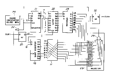
The clock extractor of Fig. 4 includes a clock
oscillator 20 for generating a.s an original clock
signal ~ a clock signal of a frequency 12. 352 htllz
corresponding to 8 times a data transmission rate (of
1.54 Mbps) of ISDN line, a counter 21 for dividing the
11
frfelueney of tl-to original clock signal <~ generat.ect at,
thc° clc>ck oscilla.t.or 2U into 1/8 to obt.a.itt a c:loclc
s i final ch 1 hav i ng a frequency of 1 . 544 Ml-lz and f or
outputting the clock signal ~ 1 from i-t.s output-
terminal (:Zc (2-~ in weight), a latch circuit 22 for
latching the count value (counter value) n of the
counter 21, a decoder 23 for decoding the count value n
(binary data) of 3 bits latched a.t the latch circuit
22, an inverter 24 for inverting tt-to original. clock
signal <h, a flip-clop 25 fc>r receiving f-Itce seI?ara.lion
wlc»-It signal C'L,Ri issued front the HAND gate 72 (refer
to rig. 3j on the basis of the inverted original c:loclc
signal rec.eivc:d from the inverter 24 a.nd for out.~:~ut.t.ing
a set output signal to the latch circuit. 22 as a lat;clt
timing signal LT for the latch 22, a shift register 26
for delaying the clock signal <~ 1 of 1. 544 MHz
(corresponding to the 1/8 divided frequency signal
having a frequency that is 1/8 of the frequency of the
original clock signal ~) issued from the counter 21
sec-~uentially at the period of the original clock signal
c~ to generate 8 sorts of delay clock signals <1>ll. to
o l.8 which are shifted with respect tc> phase
sequentially by one period of the original clock signal
a selector 29 comprising 8 AND gates 2?A to 27H and
an OFt. gate 28 for selectively outputting through the OR
ga, t.e 28 one of the 8 sorts of de lay c 1 ock s i gna 1 s ~ 11
to ~>18 corresponding to ones of the AND gates which
are opened on the bas i s of outputs dA to dH ( ort l y one
12
~0~~~~
of which is made to be "1" and rest are made to he "0"
by the latch 22 ) c>f the de cooler 23, a D type f 1 ip-f 1 op
30 for receiving the delay clock signal chli !i - 1,
2, . . . , or 8) f rom the 0R gate 28 at. the i-~er i ocl of the
clock signal <~ of 12.352 MHz and for out.putt.ing t.le
received delay clock signal a.s the extraction clack
s i gna 1 CLK s f o r sa.mp 1 i ng o f the rece i ved dat:_t s i gna 1 .
and a cross circuit 31 for intentionally crossing
output 1 roes corresponding t.o the 8 sc>r~ts of delay
c l ock s i gnal ~h 11 to d~ 18 as i 1 1 ustrated t<> dec i de the
phase of the extract i on c l ock s i final CLKs a.s the output.
of the D type flip-flop 30 on the basis of correla.t,ions
between the de 1 ay c 1 ock s i final s ~ 1 1 t.o cI> 18 a.nd the
decoder outputs dA to dH preferably or more concretely
in such a manner as convenient in receiving the data
signal. The clock oscillator 20 may be used also as a.
clock source for determining the frequency of the
associated central office. In this case, t1e clock
oscillator 20 may be commonly used for the respective
trunk circuits within the private branch exchange. It
w i 1 1 be apprec i ated from the forego i ng exp 1 a.na.t, i on flat
such clock extracting circuit and thus the first-order
group interface including the clock extractor is
provided for each of the trunk circuits within the
pr i va.t.e branch exchange.
'The operation of the clock extractor of the
embodiment illustrated in Fig. 4 will next be detailed
by also referring to Fig. 5.
13
2~~~~
la the clock extractor having such as aorangremerot.
;~a mentioned above, the counter 21 counts 3 loi i:s on tho
basis of the original clock signal ~ of 12.352 MIIz
received from the clock oscil.lat:or 20 to output. the
count. value n and also divides the frequency of~ the
original clock signal ~I> int=o 1/8 t.o ootpot from the
out.p,rt terminal C)c the clock signal ~~ 1 of 1. 544 ItlHz
correspond i ng t-.o the data transm i ss i on rate of the I SDN
1 i ne.
hleanwhi. l e. the f l ip-f lop 25, when recei vingW.lie
separation clock signal CLIti from the NAND gate 12
(refer to Fig. 3), accepts tire signal ChKi at the
fal I ing timing of the clock sigwal ~ (logic,a.lly
inverted through the inverter 24) a.nd outvput.s fr<»n its
(~ terminal a C~ signal to the latch circuit 22 as the
latch timing signal hT. This results in that the latch
c i rcu i t 22 latches the count val ue n o.f the ooo.n ter 21
a.t the rising timing of the latch timing signal h'f.
More in detai 1, as shown in Fig. 5, (a.) is t:he
separation clock signal CLKi, (b) is the original clock
signal ~ of 12.352 MHz, (c) the count value n signal
of the counter 21., (d) is the output (latched contents)
of the latch circuit 22. When the separation clock
signal CLKi rises at a time point between time points
tl and t2 as illustrated in Fig. 5(a), the flip-flop 25
outputs the latch timing signal L'T at a falling edge
(at a. time point t3) of the original clock signal <h
appearing immediately after the rising point of t:he
14
set>arat.ion clock signal. Assume at this tune the
counter 21 has a. count value n of "0". Then the la.-t.ch
circuit 22 latches the count value n of 0.
Fig. 2(e) shows the divided-frequency clock signal
~~1 (whose frequency is 1/8 of that of the original
clock signal ~~ ) issued from the output terminal Qc of
the counter 21. The divided-frequency clock signal ~~l
is applied from the counter 21 to the shift: register
26.
'The shift register 26 accepts the clock signal
~h1 at the falling timing of the original clock sigwal.
~ having a frequency corresponding to 8 times t;hal; of
l;he clock signal ~ 1 and each time the original clock
signal ~, shifts the stage by one state from a.n input
stage QA to the last stage QH. As a result, the shift.
register outputs from its stage output terminals QA to
QH the 8 sorts of delay clock signals ~ 11 to ~~18 (see
Fig. 2(f)) which corresponds to the clock signals ~~1
but. which phases are sequentially shifted by an amount
corresponding to one period. of the original clock
signal ~. These delay clock signals ~ 11 to ~~18 a.re
supplied from the shift register 26 through the cross
circuit 23 to the selector 29.
Meanwhile, since the value latched at the latch
circuit 22 is "0", the decoder 23 supplies to the
selector 29 the 8 sorts of output signals having a.
logical level of "1" appearing only at the output
terminal dA among the output terminals dA to dH and
15
having a. logical level of "U" appearing a.t the other
terminals dB t.o dH.
In the illustrated embodiment, the correlations
within the selector 29 between the 8 sorts of delay
clock signals ~ 11 to ct> 18 issued from t:he shift
reK i ster 26 a.nd the outputs dA to dll of the decoder 23
are previously adjusted by means of the cross circuit.
31 as illustrated in Fig. 4, so that the selector 29
selectively outputs, among the delay clock signals d>11
to ~ 1.8 of the shi f t register- 26, the s i.gnal ~h 16 when
the signal dA has a level "1", the signal ~hlr when the
signal dB has a level "1", the signal ~>18 when the
signal dC has a level of "1", the signal ~ 11 when the
signal dL) has a level of "1", the signal ~ 12 when the
signal dE has a level of "1", the signal ~ 13 when the
signal dF has a level "1", the signal ~ 14 when the
signal dG has a level of "1", the signal ~ 15 when the
signal has a level of "1", respectively. And in the
example shown in Fig. 5, the selector 29 selects the
delay clock signal ~~16 issued from the output terminal
QF of the shift register 26 and applies it to the flip-
flop 30 at its input terminal D.
The flip-flop 30, when applied with the delay
clock signal (delay clock signal ~ 16) thereto, accepts
the signal at every rising edge of the original clock
signal ~ and outputs such a clock signal CLKs as shown
in Fig. 5 (g) . That is, as seen from Fig. (g) and (a) .
the clock signal CLKs rises as delayed at a timing
16
2~~.~~'~~
corresponding to a phase delay of about 25°a of the
se~~a.ration clock signal CLKi with respect t.o nearly the
mid-point of the logical high level duration (pulse
width) of the signal CLKi. The clock signal C.'LKs is
sent from the c 1 ock extractor of Fig. 4 to the c 1 ock
generator 6 (see Fig. 1) as a clock signal for sampling
of the received data signal, as already explained
above.
The operation and ft.tnction of the clock ext.ract.or
of the present embodiment are summarized as follows.
(1) The 8 sorts of different delay clock signals ~l>11
to ~ 18 slightly shifted to each other in ~?hase
are generated at al 1 t i rues.
(2) Each time the flip-flop 25 detects the separation
clock signal CLKi, the selector 29 selects one of
the 8 sorts of delay clock signals <1> 11 to ~~ 18
which allows most faithful reproduction of the
continuity of the separation clock signal CLKi on
the basis of the detection timing (pha.se).
(3) The selected clock signal is outputted as the clock
signal CLKs for sampling of the received data
s i gna 1.
(4) During a period in which the separation clock
signal CLKi is not detected, the delay clock
signal having the phase selected immediately
before the absence of the detection o.f the signal
CLRi is continuously outputted as the clock signal
C:LKs.
li
~0~.~~~
15) 'The at-rove selected delay clock signal and thi.rs the
above output clock signal CLKs is prc,viously
adjusted at. the cross circuit 31 in such a manner
as convenient t.o a.ccept. the data of the received
signal, t.lnat. is, so that the clock signal C'Llis
rises a.t the timing corresponding to nearly t:he
mid-~Ulllt. of the pulse width of the sepa.ra.tion
c 1 oc lc s i gna. l CLIi i .
I n th i s wa.y, the c 1 ock ext.ractcw of ttte present
cmlooclirne:nt can easily output a clock signal that allows
accurate reading-in operation of the dat:a of the then
received signal a.s the extra.ct.ioti clock signal C',Llts
through full non-adjusting opera.t.ion.
In thi s connec t i on, i t i s unnecessary f or tlc
cle>ck signal CLIis to rise at the timing strictly
accurately coinciding with the mid-point of the pulse
width of the separation clock signal CLKi. In other
words, so long a.s the clock signal C,'LILs rises anywhere
w i th i n the dura,t. i on of the separat i on c 1 c>ck s i gna l CLIZ i
having a logical level of "1", it is possible to
accurately read in the corresponding clat.a. of the
received signal. In this case, it goes without. saying
that the clock signal CLKs is preferably set. t.o rise at.
the timing corresponding to nearly the mid-poitrt of the
pulse width of the separation clock signal CLKi as in
the foregoing embodiment, because such setting provides
a high allowance in reading the received sigll.~l data.
For our easy understanding of the present
18
emhod i men t., cons i derat i on w i l l next. lie d i rec ted t.o how
j i tter affects the c i rc.ui t. c>f the present. embodiment..
Far example. when a fitter takes place in the data of a
received signal, the separation clock sib°nal CLIIi
having a relatively long pulse width at the 1_~eginning
and then having a relatively short pulse wic_it.h is
detected. In the case of the separation clock signal
CLlii having a relatively long pulse width, the rising
position of the clock signal CLKs is shifted forward of
the mid-point of the pulse width of the signal CLIii.
When the rising position of the clock CLKs is shifted
too forward, there is a possibility that. the clock
s i gnal CLKs r, i ses before generat i on of the sepa.ra.t i on
clock signal CLKi having the next short. pulse width.
In the case of the above example, the extraction
clock signal CLKs rises at a. time point t6. Thus, when
the fitter causes the data width of the received data
signal, i. e. , the pulsed width of the sepa.ra.t.ion elc>cIc
signal CLKi to be short, it is possible to extract the
data. immediately before the time t6.
In the foregoing example, further, a. portion of
the pulse width of the separation clock signal CLKi
(refer to Fig. 5 (a) ) between time points t3 t.o tO
corresponds to 3/8 of the pulse width and a portion of
the pulse width between the time points tl and t3
corresponds to a. sampling error, so that the then
allowable fitter range is below 37.5°0 (3/8 x 100)
including the rising and falling times of the
19
2~~~'~3
sfy~~rrat.ion clod: signal CLKi. In other vaords, sc> long
<rs the allowable fitter range is below 3i.5°o including
t.lic rising and falling times of the separat.iorr clock
signal CLIsi, the fitter wi 11 not affect. the operation
of the embod i ment c i rcu i t. ~1'hus, when the ex tract. i on.
evlocli signal C"I,Iis is set to rise a.t. a tirnE~ E>oint t.i in
t.hE~ circuit of the embodiment, it is possible t.o obt.a.in
a fitter allowably range of below 50°b (= 4/8 x 100).
()n the cont.ra.ry, the j i tter i s usual ly prescr i bed
t.o In a be 1 ow 20 and several °~ i nc 1 ud i ng the r i s i ng a.nd
falling times of the separa.t.ion c.loc:l. sigwa.l.
'I~trc~reforc~. i t- vai 1 1 be apprec i ated that the cv i rcnri t of
t.lre present. embodiment can sufficiently wit.hst,and
~pra.ct, i cal 1 y even the general. i on of such j i t ter. In
addition, when it is required tc> adjust the rising time
of the extraction clock signal CLhs, e.g. a.t the time
point t7, this ca.n be easily realized by changing the
crc>ssed ccmnection c>f the cross circuit 31.
Every when the received signal data is subjected to
a fitter, this influence can be sufficiently avoided
through the c i rcui t of the present embodiment. ; but. when
an abnarma 1 wavef orm occurs i n the rece i ved da.t.a s i gna 1
due to noise, there is a danger that; the occurrence of
the abnormal rvaveform deteriorates the continuity o.f
the clock signal CLKs is in the circuit c>f the present
embod i ment.
Shown in Fig. 6 is a clock extracting circuit in
accordance with another embodiment of the present
20
invc:ntian, which, even when such an abnormal waveform
acctrrs in the received data signal due t.a noise, can
minimize the influence of the abnormal wa.vefarm.
In the circuit of Fig. 6, a D type flip-flap 32
a.ccept.s a.t the rising edge of the original clock signal
<h and sets therein the latch timing signal L'f that is
issued from the flip-flap 25 and t.ha.t rises at. the tune
paint t3 in the example of Fig. 5; whereas, a. D type
flip-flop 33 accepts and sets therein an output of the
fl ip-flap 32 a.t the fal l ing Edge. of the original clock
signal ~. Accordingly. flip-flops 32 a.nd 33 output.
signals which rise at the time paints t4 a.nd t5 in the
example of Fig. 5, respectively.
The circuit of Fig. 6 further includes a.n up/down
counter 34 for maintaining, ,counting up or counting
down a value nb received at its input terminal A an the
basis of the output of the flip-flap 32 rising at the
time t4, a latch circuit 35 far latching an output
value of the up/dawn counter 34 an the basis of the
output of the flip-flop 33 rising at the time paint t5,
and a comparatar 36 for receiving at its input, terminal
A the value n latched at the latch circuit 22 a.nd also
receiving at its input terminal B the value nb latched
at the latch C1I'Clllt 35 to compare these values.
'fhraugh the loop operation of these elements, the noise
processing operation of the clack extractor of the
present embodiment is substantially carried out.
More specifically, the up/down Gaunter 34
21
wJ->r~tit-ively carries out the following o~>era.t.ions (a.)
t r., f c ) i n a.ccorda nce w i th a- cornpar i sc_~n c>u l-.~»1 t of the
compa.ra.t.or 36, each time the f 1 i p-f 1 op 32 r i ses.
la.) when the outputs A a.nd B satisfy a re.l~~t.ic>nship A =
B, the up/down counter 34 ma.inta.ins thc: value nb
received a.t the input terminal A.
(b) When the outputs A a.nd B satisfy a relationship A >
B. the up/down counter counts up the value nb
rece i ved at. the i nput. term i na l A.
lc) EVhen the out-puts A and B sa.-tisfy a relationship A <
B, the up/down counter counts down t:he value nb
received at. the input terminal A.
It is here to be noted that since the count value
c>f the up/down counter 34 is latched at the latch
circuit 35 at a timing after the counting, that is, at
the time point t5 in Fig. 5, the value nb a.s the output
of the latch circuit 35 indicates the previously
CULirlted value and is applied to the comparator 36 a.nd
the up/down counter 34. The operation of these
elements 36 and 34 will be summarized as follows.
(1) The comparator 36 compares the previous count value
nb with the current count value n, that is,
monitors the periodicity of the input, separation
clock signal CLKi.
l2) When nb - n, the up/down counter 34 appl ies the
count value (nb - n) to the decoder 23 as i t is.
The value applied to the decoder 23 is used in the
next cycle as the previc>us count value nb.
22
2~~~
(3) When nb > the up/down counter applies value
n, a.
correspond i ng the CUllI'lt val ue nb m t.o
to i nus 1 t.h
decoder 23. The value applied t.o the deco der
23
i s used i n the ext cyc 1 a as the pi~ev count
n i oi_is
va 1 ue nb.
When n b < n, the up/down counter applies value
a
corresponding to the count value nb plus 1 to the
decoder 23. The value applied to the decoder 23
is used in the next cycle as the previous r_ourit
va 1 ue nb.
For example, in the event where an abnormal. waveform NZ
takes place in the separation clock signal C.'Llii due to
noise as shown irn Fig. 7(a) a.nd this causes the then
count value n (corresponding to the count va.l.ue n of
the Fig. 5(c)) to become extremely different value (3
-'6) as shown in Fig. 7(b), through the above operation
(the above operation (4)) a value n' actmally applied
in the current cycle to the decoder 23 and to be used
in the next cycle as the previous count. value nb is
averaged down to a value (3 -;4) that is suppressed to
its minimum extent in its change as shown in Fig. '7(c).
Thereafter, when the count value returns to the normal
level (when the count value n returns to 3 in the same
example), the above operation (corresponding to the
operation (3)) causes the value n' to be also returned
to a normal value (4 --~ 3).
Tn this wa.y, in the embodiment of Fig. 6, even
when the waveform of the received data signal
23
2~~~43
(sepa.ra.t.ion clock signal) is made a.bnorma.l due t.o
no i se, the va.l ue to be appl i ed to the decoder 23 as
well as the value referenced as the previous count.
value nh arc, adjusted every time. ~lccorctingly, t.lne
clock signal CLIis is not subjec~t.ed to a.rt extreme. phase
co l l a.pso and t.lnus can be extra.c t.ed i n such a. form tha r.
can maintain its ideal continuity t.o it.s maximum
ex t ent.
A1 though the embodiment of Fig. 6 has been
arranged so tlia-t the clock synchronization (phase) is
so-oa.lled ~'smoc~ttted" through .~ddit.ion or subt.ra.ction of
" 1'~ when vi ewed wi th respect to a 1 ong per i oct of ti me.
Ilon~ever, such a.n a.rrangetnenl.: as shown in Fig. 8 may be
of cJottrse possible that an LSI such a,s a. digi ta.l signal.
processor (DSF') 4U is used to "average" count values
(outputs of the latch 22) for a previous constant
period and the "averaged" count value is transferred to
the decoder 23 when the count value latched at the
latch 22 is different front the previous one. This
also enables t;he smoothing of an abnormal waveform
caused by noise or the like and thus the a.cquisi.lion of
the clock signal CLKs having a stable period (Phase).
The same elements in Figs. 6 and 8 as those in Fig. 4
arcJ denoted by the same reference numerals arid
expla.n.a,ti.on thereof is omitted.
Although the original clock signal ~> has been set
l,o have a frequency of 12. 352 MHz, the frequency
division number has been set to be 21 i.n the counter 21
24
2~~~4~3
and the number of stages in the shift register 2E> has
keen set to be 8 in the foregoing embc>dimen-t.s; the
present inventiUll 1S nUt l united to the pa.rt.icula.r
values and these values may be arbitrarily selected
according to the desired accuracy of please of the
ext.ra.clion clock signal CLKs, as a. matter of course.
25