Note : Les descriptions sont présentées dans la langue officielle dans laquelle elles ont été soumises.
~ `
2~ 7~7
SWITCHING AMPLIFIER
Fiel~ of the Invention
The invention pertains to methods and apparatus
for processing audio signals. More particularly, the
invention pertains to a high efficiency switching
amplifier useful in-a portable battery operated device.
Backqround of the Invention
High efficiency switching amplifiers usable to
amplify audio frequency signals are well known. One such
amplifier system is disclosed in U.S. Patent No. 3,185,768
to Cudahy entitled Amplifier Circuit.
Known switching amplifier systems generate a
pulse width modulated switching signal in response to the
applied audio input signal. The modulated signal includes
components that replicate the audio input signal. In
addition, it includes high frequency components associated
with the frequency of the switching signal and its
harmonics.
The modulated switching signal can be used to
provide input signals to solid state switches. The solid
state switches provide an output signal to a load.
Where the load has an inductive component, or
there is an inductive filter in series with the load, the
higher frequ~ncy components of the load current will be
attenuated.
Because of limitations on the maximum value and
the quality of the inductive components there can still
be an appreciable current flow associated with the higher
frequency components of the output signal. This current
flow is especially apparent for small amplitudes of the
audio input signal.
The use of an inductive filter is undesirable
in that it increases amplifier size and weight. It also
increases amplifier cost.
:., .,, ., : ,; - :
.~ -:- . , . - - . - .
.~ ~ - - ,
~? ~
3 7 2 7
-
In addition, in the absence of a modulating
audio input signal, the switching signal often appears at
the load as a square wave. This square wave has an
amplitude corresponding to the peak to peak output
capability of the amplifier at the frequency of the
switching waveform.-
Such units tend to be used in a portable,battery powered environments. As a result, it is
particularly desirable to minimize size and weight and
losses of energy from the battery particularly when the
input audio signal has substantially zero amplitude.
Summary of the Inventio~
In accordance with the invention, a high
efficiency switching amplifier provides an amplified
representation of an input signal to a load. The
amplifier includes circuitry for generating a selected
high frequency clock waveform. The high frequency clock
waveform is coupled to first and second pulse width
modulators. The input signal to be amplified is also
coupled to the two modulators. An input to one of the two
modulators is inverted. Each modulator generates a pulse
width modulated switching waveform in response to
instantaneous values of the input signal.
A push-pull bridge output switching circuit is
coupled to the output of each of the modulating circuits.
The load is coupled across first and second terminals of
the output bridge.
An amplified representation of the audio
frequency input signal appears across the first and second
output terminals of the push-pull bridge output stage and
is delivered to the load. If the load is inductive, the
current due to the high frequency components of the pulse
width modulated switching signals will be attenuated
providing high efficiency.
,.,: ., ,~. .. .
;~ : :
3 Y~ 2 ~
,
A particular advantage of the present amplifier
is that if the input signal has a value substantially
equal to zero, the amplified representation delivered to
the load also has a value substantially equal to zero.
No pulsed or switching signal is provided to the load in
this condition.
The pulse width modulators in one embodiment
each include a comparator for comparing the amplitude of
the input signal to the amplitude of the high frequency
clock waveform. The input to one modulator is an inverted
representation of the input electrical signal.
The clock waveform can be a triangularly shaped
waveform. Alternately, the clock waveform can be a saw-
tooth. In an alternate embodiment of the invention, the
high ~requency clock input to one of the comparators could
be inverted instead of inverting the input electrical
signal.
The push-pull, bridge output stage of the
amplifier includes four switching elements, such as field
; 20 effect transistors. The load is coupled across the first
and second output terminals of the bridge. As a result
of alternately switching various pairs of the switching
elements in the bridge, a tri-level output signal can be
applied to the load even though only a single source of
electrical energy is used to power the amplifier.
- In yet another embodiment, the modulators can
each include a voltage or current controlled pulse width
generator. The high frequency clock signal can be coupled
to a clock input to each generator. The input signal can
be coupled to the pulse width input of one generator. An
inverted input signal can be coupled to the pulse width
input of the second generator. The pulse width modulated
output sequence from each of the two generators can be
coupled to a respective input of the bridge output stage.
~ ~3 ~ 3 ~
In yet another embodiment of the invention, a
system for processing an acoustical signal includes
circuitry for sensing the acoustical signal and for
generating an electrical signal in response thereto. The
electrical signal is amplified in a switching amplifier
having first and second modulator circuits interconnected
as described above. Output from the switching amplifier
is coupled to a transducer for converting the amplified
electrical signals to an output acoustical signal.
Numerous other advantages and features of the
present invention will become readily apparent from the
following detailed description of the invention and the
embodiments thereof, from the claims and from the
accompanying drawings in which the details of the
invention are fully and completely disclosed as a part of
this specification.
Brief Description of the Drawin~s
Figure 1 is a block diagram schematic
illustrating a switching amplifier in accordance with the
present invention;
Figures 2A-2C are a set of graphs illustrating
waveforms present in the switching amplifier of Figure 1
as a function of time;
Figure 3 is a detailed schematic of a switching
amplifier in accordance with the present invention;
Figure 4 is a block diagram of a hearing aid and
audio processing unit in accordance with the present
invention;
Figure 5 is a partial block diagram of an
alternate modulator configuration usable in a switching
amplifier in accordance with the present invention;
Figure 6 is a partial block diagram of yet
another modulation system usable in a switching amplifier
in accordance with the present invention; and
~',' ' ~' ~ . .
~sS:, .. .. .
3 ~ ~ ~
Figure 7 is an alternate output stage usable
with any of the previously noted modulators.
Detailed Description of the Preferred Embodiments
While this invention is susceptible of
embodiment in many different forms, there is shown in the
drawing and will be described herein in detail a specific
embodiment thereof with the understanding that the present
disclosure is to be considered as an exemplification of
the principles of the invention and is not intended to
limit the invention to the specific embodiment
illustrated.
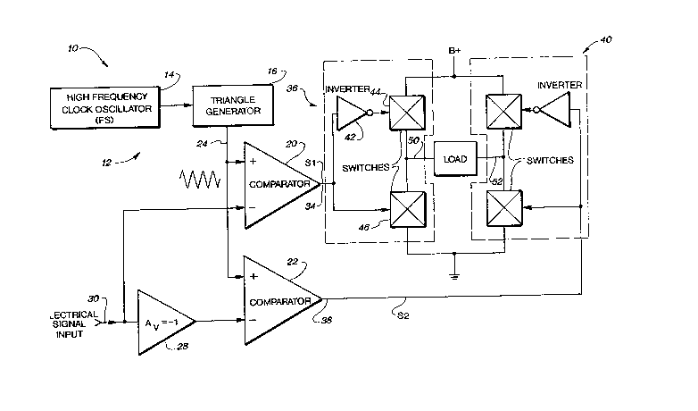
Figure 1 illustrates a block diagram of a high
efficiency switchiny amplifier system 10 in accordance
with the present invention. The system 10 includes a
source 12 of high frequency clock or comparison signals.
The source 12 includes an oscillator 14 which
provides a pulse train of electrical signals to a
triangular waveform generator 16. The generator 16, in
combination with the clock oscillator 14, generate a
triangularly shaped waveform of a frequency on the order
of 100 kilohertz.
The system 10 includes first and second
comparators 20 and 22. Output from the triangular wave
generator 16 on a line 24 is supplied to a positive input
to each of the comparators 20 and 22.
; The system 10 also includes an inverter circuit
28. The inverter circuit 28 can be implemented as an
operational amplifier configured to have a gain of minus
one.
~n electrical input signal to be amplified is
coupled to the system 10 at an input port 30~ The input
port 30 is in turn coupled to a negative input of the
comparator 20 and the input of the inverter 28. Output
from the inverter 28 is coupled to a negative input of the
comparator 22.
, ~
As is apparent from the schematic diagram of
Figure 1, comparators 20 and 22 receive the same
comparison waveform from the generator 16. However, as
a result of the inverter 28, the modulating signals
applied to the comparators 20 and 22, respectively, are
out of phase.
Output from the comparator 20, a pulse width
modulated pulse train S1, on a line 34, is in turn coupled
to a first switchin~ element 36. Output from the
comparator 22, a pulse width modulated pulse train S2, on
a line 38, is coupled to a second switching element 40.
The elements 36, 40 form a four element push-
pull output bridge. Since a bridge output stage is
incorporated into the amplifier 10, only a single source
of electrical energy (B+) is needed to produce a tri-level
output signal.
The switching element 36 includes an inverter
42 with an output line coupled to a first transistor
switch 44. Output from the comparator 34 is coupled to
a second transistor switch 46 in the switching element 36.
The switching element 40 is identical to the switching
element 36.
Output conducting members 50 and 52 are each
coupled to the transistor switches of a respective one of
the switching elements 36 and 40. For example, conducting
member 50 is coupled to semiconductor switches 44 and 46.
The same voltage source, which could be a low voltage
mercury battery, on the order of 1.3 volts, or a higher
voltage 3 volt battery is coupled to each of the switching
elements 36 and 40.
An output signal is generated across the
conducting members 50 and 52. A load L can be connected
therebetween. As is described subsequently, an amplified
representation of the electrical signal applied to the
- ~ ~ Ç~ R ~ r~ q
input port 30 appears across ths conducting members 50,
52 and hence is applied to the load L.
The switching amplifier system 10 of Figure 1
is particularly advantageous in that the circuitry thereof
substantially reduces the amplitude of high frequency
switching components-in the output signal appearing across
the conducting members 50, 52. As a result, no separate
inductive filter is needed if the load L inherently has
an inductive impedance. This is usually the case for
hearing aid receivers intended to provide an acoustic
frequency response within the normal hearing range on the
order of 100 hertz to 10,000 hertz.
Figure 2 illustrates some of the waveforms
associated with the system 10 on lines 50, 52 for
different modulation conditions. The switching elements
36 and 40 as configured in Figure 1 and driven by
comparators 20 and 22 combine the electrical signals on
the line 34 and the line 38 by subtracting one from the
other at the conducting members 50 and 52.
Figure 2A illustrates the outputs on the lines
50, 52 where the input electrical signal on the input port
30 produces a 60~ positive modulation condition. The
output graph of lines 50-52 is the push-pull output signal
applied to the Load L. It corresponds to the difference
of the signals on the lines 50, 52.
Figure 2B illustrates the outputs on the lines
50, 52 where the input electrical signal on the input port
30 has a zero instantaneous value thereby producing an
unmodulated condition at the Load L. As can be seen from
Figure 2B, the outputs on the lines 50 and 52 are ;
identical.
Hence, the difference between the lines 50 and
52 results in an essentially zero value amplitude signal
delivered to the Load L. This zero amplitude signal is
particularly advantageous in that no switching signal is
''::~'
:
I~J ~ .,L 3 ~ 2 7
applied to the load when the input voltage has a value of
zero volts.
The waveforms of Figure 2C illustrate the
outputs on the lines 50, 52 where the input electrical
signal produces a 60% negative]modulation condition. The
output graph of the-lines 50-52 is the push-pull output
~ignal applied to the Load L.
Figure 3 is a schematic diagram of a circuit in
accordance with the system 10 of Figure 1. Elements o~
the amplifier system 10 of Figure 3 which correspond to
elements of Figure 1 have been assigned the same
identification numeral. In the schematic of Figure 3, the
clock oscillator 14 has been implemented with a series
coupled pair of inverters. The triangle generator 16 has
been implemented with a D flip-flop in combination with
a resistor and a capacitor.
The output bridge, composed of switching
elements 36 and 40 has been illustrated in Figure 3
implemented with a commercially available CMOS element
type 74HCU04. The comparator elements 20, 22 illustrated
in Figure 3 are open collector output devices which
require output load resistors 21 and 23. Alternately,
comparators could be used having pull-up and pull-down
(totem pole) outputs for lower power dissipation.
Figure 4 is an overall block diagram of a
hearing aid or an acoustic processing system 60. The
acoustic processing system 60 includes an input microphone
62. The input microphone 62 converts an acoustic input
Pl~ to a corresponding electrical signal.
The electrical signal from the microphone 62 can
be amplified in a preamplifier 64. Output from the
preamplifier 64 on the line 30 corresponds to the input
to the switching amplifier 10.
0ut:put from the switching amplifier 10 on the
3S lines 50, 52 can be applied to a receiver 66. The
..
.
:
receiver 66 converts electrical signals on the lines 50,
52 to an acoustical output P~T.
The amplifier system 10 has several significant
advantages when compared to a standard Class D type
switching amplifier. One of the advantages of the system
10 is that the high frequency components of the switching
signal and its harmonics which are present in the load
output voltage on the lines 50, 52 are substantially less
than for the case of a standard Class D type switching
amplifier. Further, when the input voltage on the input
terminal 30 to the system 10 is on the order of zero volts
there is substantially no switching signal applied across
the output conductors 50, 52 as would be the case of
standard Class D switching amplifiers. In addition, for
low-level inputs, the system 10 will draw less current
than will conventional class D-type amplifiers.
Finally, with respect to the detailed
implementation of the system 10 illustrated on Figure 3,
variations on the reference voltage coupled to a line 28a
of the inverter 28 do not cause a net DC current to flow
through the Load L. Variations in the reference voltage
VR appear as only a common mode ~ffset in the output on
each of the lines 50, 52. In a standard Class D
amplifier, such variations in the value of the quiescent
operating point would result in a DC current flowing
through the Load L.
An alternate modulator system 70 usable with the
amplifier 10 is illustrated in Figure 5. The modulator
system 70 includes the comparators 20 and 22 both of which
are coupled to the input port 30. The modulator system
70 also includes the triangular waveform generator 16 and
inverting operational amplifier 28. However, in the
modulator system 70, the output of the triangular wave
generator 16 is inverted before it is coupled to the
comparator 22.
3 ~ 2 ~
outputs from the comparators 20, 22 the signals
Sl, S2 on the lines 34 and 38 can be coupled to the push-
pull bridge output stage 36, 40 illustrated in Figure l.
Figure 6 illustrates another modulator system
74. The modulator system 74 :includes a source of high
frequency clock puls~s 76. Output pulses from the source
76 are coupled to clock inputs of variable pulse width
generator circuits 78 and 80. The variable pulse width
CirGUitS 78 and 80 could be implemented, for example, as
mono-stable multivibrators.
As illustrated in Figure 6, the width input to
each of the generators 78 and 80 is coupled respectively
to the input signal and the inverted input signal. The
two pulse width modulated waveforms S1, S2 generated on
the lines 82 and 84 can in turn be coupled to the push-
pull bridge output stage 36, 40 of Figure l to drive the
~;~ load.
Figure 7 illustrates an alternate, single ended,
output stage 9o. The output stage 9o utilizes a positive
and a negative source in combination with three non-
inverting semiconductor switching elements 92, 94 and 96.
Inputs to the switching elements 92, 94 and 96
are provide via coded input signals on the lines 92a, 94a,
and 96a. The coded inputs are derived from pulse width
modulated output waveforms Sl and S2 and can be generated
using any of the previously discussed modulator systems
in combinat~ion with conventional digital logic.
The outputs from the switching elements 92-96
are coupled together at an output node 98 and in turn
coupled to the load. As was the case with the push-pull
output stage 36, 40 previously discussed, the output stage
90 provides a tri-level output to the load. When the
instantaneous value of the input electrical signal is
substantially zero volts, the output stage 90 delivers
substantially zero volts to the load.
~il,,":. ~
3~7J~
. .
It will be understood that the present amplifier
system can be used not only for the purpose of ampli~ying
audio frequency signals but for the purpose of amplifying
other signals. Other examples include control signals
such as could be used to control the velocity of a
rotating shaft of a motor. In addition, it will be
understood that the present amplifier is useful wherever
high efficiency, portable, battery-powered operation i5
re~uired.
From the foregoing, it will be observed khat
numerous variations and modifications may be effected
without departing from the spirit and scope of the novel
concept of the invention. It is to be understood that no
limitation with respect to the specific apparatus
illustrated herein is intended or should be inferred. It
is, of course, intended to cover by the appended claims
all such modifications as fall within the scope of the
claims.
.
.: